


1. Introduction
Despite the rapid progress made in group III nitride based semiconductor film growth Reference Nakamura, Senoh, Iwasa and Nagahama[1], better substrates are still needed for high quality epitaxial growth. Currently, there is worldwide interest in producing high-quality single crystals suitable for nitride based electronic and optoelectronic devices. The ideal substrate should be lattice matched, isomorphic, and thermal expansion coefficient matched to the film as much as possible. Single crystal AlN is attractive as a substrate for group III-nitride epitaxial growth due to its relatively small lattice constant mismatch along the a-axis (−2.5%) with GaN, good thermal stability (melting point >2500 °C), high resistivity and similar coefficient of thermal expansion Reference Lu, Bhat, Lee, Slack and Schowalter[2]. To date, bulk AlN single crystals are limited in sizes to diameters below 15mm Reference Schowalter, Shusterman, Wang, Bhat, Arunmozhi and Slack[3].
Bulk AlN crystals are most commonly produced by vapor transport (sublimation) from an AlN source. This technique was most successfully developed by Slack and McNelly Reference Slack and McNelly[4], Reference Slack and McNelly[5] in the mid-1970's. Large AlN single crystals, up to 1 cm long and 0.4 cm in diameter, were grown by self-seeding from the sharp tip of sealed tungsten crucibles heated in an radio frequency induction furnace. Recently, Schowalter etal Reference Schowalter, Shusterman, Wang, Bhat, Arunmozhi and Slack[3] demonstrated good quality AlGaN epitaxy on bulk AlN crystals produced by self-seeding.
Seeding bulk AlN growth on silicon carbide substrates instead of self-seeding offers several potential advantages including the availability of large diameter seed crystals (up to 100 mm) for rapid process scale-up, and better control of the crystal polarity, through the choice of the SiC seed crystal polarity (C or Si polarity). Balkas et al Reference Balkas, Sitar, Zheleva, Bergman, Nemanich and Davis[6] first produced thick (< 1 mm) AlN films on 10×10 mm2 6H-SiC substrates in a resistively heated graphite furnace. Their results presented three problems with 6H-SiC as seed crystals: the decomposition of the SiC substrate at high crystal growth temperatures, the formation of individual grains in the AlN crystal, and cracking of AlN due to differences in the thermal expansion coefficients of AlN and SiC.
The author's previous study of pure AlN grown on SiC substrate showed that direct growth on Si-polarity as-received SiC substrates was discontinuous, marked by sparse nucleation and slow lateral growth of nuclei Reference Shi, Xie, Liu, Liu, Edgar and Kuball[7]. Multiple hexagonal AlN grains typically formed after a long growth time (more than 3 hours) due to nucleation at several sites and island growth mode. A technique for suppressing SiC decomposition and grain boundary formation in the AlN films was developed by first depositing an AlN buffer layer by MOCVD before sublimation growth Reference Shi, Xie, Liu, Liu, Edgar and Kuball[7].
The current paper describes a solution for a third problem: cracks. The tensile stress due to thermal expansion coefficient mismatch between the AlN layer and the SiC substrate caused cracking during cooling. Cracks are effectively reduced by forming an (AlN)x(SiC)1−x alloy on the SiC substrate with AlN MOCVD buffer layer, then depositing pure AlN on the alloy seed by sublimation because its thermal expansion coefficient is intermediate between SiC and AlN, hence the thermally generated stress can be reduced. Besides, the presence of silicon and carbon in the source material reduces or eliminates the decomposition of the SiC substrate during sublimation crystal growth, enabling longer duration crystal growth.
(AlN)x(SiC)1−x alloys are of interest not only as the seeds for pure AlN single crystal growth, but also as promising semiconductors themselves because the physical and electronic properties can be controlled by selecting a specific AlN:SiC alloy composition. The research group at the University of Dagestan extensively investigated the properties of epitaxial (AlN)x(SiC)1−x films grown by the sublimation method on 6H-SiC substrates from sintered polycrystalline SiC-AlN sources in argon and nitrogen mixtures through the full compositional range x Reference Safaraliev, Tsvetkov and Tairov[8], Reference Safaraliev, Sukhanek, Tairov and Tsvetkov[9], Reference Ofitservoa, Kurbanov, Nikitina, Sorokin, Safaraliev, Tairov and Tsvetkov[10]. The energy band gap can be controlled by the alloy composition over a very wide range (from 2.9 eV for pure SiC to 6.2 eV for pure AlN), the band transition is direct for x>0.7 and both n- and p-type conductivity are possible. In reference Reference Safaraliev, Tsvetkov and Tairov[8], the composition of the epitaxial (AlN)x(SiC)1−x was measured to have a linear relationship with the source materials (only for aluminum however) but no detailed experimental data was provided to support this relationship. A recently approved patent Reference Hunter[11] reported the growth of bulk (AlN)0.7(SiC)0.3 single crystals 2 inches in diameter and 46-50 mm thick by the same technique from a polycrystalline (AlN)0.7(SiC)0.3 source. The chemical composition analysis of the grown crystal was not reported, only the nominal composition (AlN)0.7(SiC)0.3 of the source. The crystal quality characterization was also not reported in this patent.
All the previous studies of (AlN)x(SiC)1−x alloy growth used only as-received SiC substrates without MOCVD buffer layers; they used polycrystalline sources in contrast to our use of only mechanical mixture of AlN and SiC powders Reference Safaraliev, Tsvetkov and Tairov[8], Reference Hunter[11]. The structural investigations reported in Ref. Reference Safaraliev, Tsvetkov and Tairov[8] show the morphologies and structural qualities of the heteroepitaxial layers deteriorating with the AlN content. When x< 0.5, the perfection of the epitaxial layers of (SiC)1−x(AlN)x was comparable with that of the SiC substrate. Increasing x (x> 0.5) deteriorated the morphologies of the epitaxial layers and caused the appearance of a mosaic structure. On using a 90wt% AlN source, heterogeneous growth of AlN on SiC was observed. Patent Reference Hunter[11] reported large single crystals grown from (AlN)0.7(SiC)0.3 polycrystalline source on a bare SiC substrate. However, we found that AlN single crystals could not be produced on bare SiC substrates in our furnace using the growth parameters given in Ref. Reference Hunter[11].
In this paper, a new technique employing SiC single crystals as substrates for bulk crystal growth of AlN by the sublimation method was developed. The method consists of (1) depositing an AlN buffer layer on the SiC substrate by metal organic chemical vapor deposition (MOCVD) below 1100°C, (2) forming an (AlN)x(SiC)1−x alloy film on the above AlN film by condensing vapors sublimated at a temperature of 1800°C from a source mixture of AlN-SiC powders, followed by (3) condensing vapors sublimated from a pure AlN source (at 1800°C). How the first two steps help solve the three problems for the AlN sublimation growth on SiC substrate is illustrated by initial nucleation studies of alloys on SiC substrates with and without MOCVD buffer layers. The high quality AlN crystal obtained from the above three steps was characterized by SAM (Scanning Auger Microscopy), Raman scattering and X-ray diffraction techniques.
2. Experimental procedures
2.1 Crystal growth
Sublimation growth experiments were conducted in a resistively heated furnace using tungsten wire mesh heating elements. The seed and source were enclosed in two concentric tungsten crucibles to contain the Al vapor as it will seriously damage the tungsten heating elements. The source materials are AlN (99.5%, Tokuyama Soda Co., LTD, Japan) and SiC powder (99.8%, Alfa Aesar, USA). The source materials for alloy growth with proper AlN:SiC ratio were thoroughly mixed in an alumina mortar and sintered at 1800°C and 500 torr in the same furnace before sublimation growth. The θ−2θ x-ray diffraction pattern of source materials after 60 hours sintering still showed the mixture of AlN and SiC powders instead of polycrystalline (AlN)x(SiC)1−x alloys. The seed holders were sintered AlN with approximately 1% oxygen as the main impurity as analyzed by a standard inert gas fusion method (TC-136, Leco Co.). The as-received (0001) 6H-SiC silicon polarity on-axis wafers were cut into about 2cmx2cm substrates. All the substrates were ultrasonically degreased in organic solvents, rinsed in deionized water , and blown in dry nitrogen before loading into the furnace. The distance between the source and the substrate was kept constant at 2mm. The backside of the seed was covered by a sintered AlN cap to reduce SiC dissociation.
Information about the furnace and growth process has been described in detail in Ref. Reference Shi, Xie, Liu, Liu, Edgar and Kuball[7]. The growth ambient was 99.9999% pure nitrogen, and the background pressure during growth was 500 torr. The in-situ growth temperature was measured by an optical pyrometer focused on the top lid of the outside crucible. According to the pre-measured temperature profile, at our experimental condition the source temperature was about 1800°C and the source-substrate temperature difference was about 10°C for 2mm source-substrate distance. The growth temperature was kept constant for all growths by fixing the furnace output power during the crystal growth so the results could be fairly compared.
The thickness of samples from lengthy growths was measured with a micrometer (the accuracy is about 1μm). The average growth rate was about 5 μm/hr at 1800°C and 500 torr. Therefore, the nominal thickness of the samples grown at the same experimental condition for 15, 45 and 120 minutes was 1.25, 3.75 and 10 μm, respectively, assuming constant growth rates for the whole growth process.
2.2 Buffer layer preparation by MOCVD
The AlN buffer layer was grown in a vertical MOCVD reactor at low pressure (76 torr). Before loading into the reactor, the 6H-SiC substrates were cleaned using the same standard cleaning procedure as described above. Trimethylaluminum (TMA) and ammonia (NH3) were the Al and N sources, and Pd-cell purified H2 was the carrier gas. The substrates were preheated at 1100 °C for 10 minutes in 3 slm of H2 for surface cleaning. Then the AlN films were deposited at the same temperature under H2, NH3 and TMA flow rates of 3 slm, 3 slm and 30 sccm, respectively. An approximate 2 μm thick AlN buffer layer was obtained for the 4 hour growth.
2.3 Characterization
The as-grown AlN crystals were first characterized by Nomarski differential interference contrast microscopy (NDIC) at magnifications of 60X.
The relative chemical composition was characterized by scanning Auger microscopy (SAM) using a Physical Electronics PHI680 Auger Nanoprobe operated at a less than optimal 3kV or less because of the charging problem. To ensure the accuracy of composition measurement, samples were sputtered by argon ion for several minutes until oxygen could not be detected.
X-ray diffraction measurements were conducted using a Scintag PTS four-axis goniometer diffractometer with Cr Kα radiation (25kVx8mA) and a high purity germanium solid state detector. The lattice parameters and crystal qualities were analyzed by x-ray diffraction (XRD) of both symmetric (0002) and asymmetric (11
Micro-Raman spectra were obtained using a Renishaw UV micro-Raman system with the 325 nm line of a HeCd laser as the excitation source. The spot size and the spectral resolution were 1−2 μm and 3−4cm−1, respectively.
3. Results
3.1 Nucleation studies of (AlN)x(SiC)1‒x alloys on 6H-SiC substrates
The initial nucleation of the alloy on the SiC substrates with AlN MOCVD buffer layers was continuous and smooth. In contrast, alloy films grown on bare SiC substrates under our experimental conditions produced only discontinuous films regardless of the source AlN:SiC ratio. To make the experimental results comparable, 1:1 molar ratio mixtures of AlN and SiC powder sources were deposited on two SiC substrates, one with and one without AlN MOCVD buffer layers during the same growth run with growth times of 15, 45, 120 minutes and 100 hours, respectively. Their optical micrographs are shown in Figure 1 denoted by (1), (2), (3) and (4) in the sequence of the growth time increase.

Figure 1. Optical micrographs of (AlN)x(SiC)1‒x alloy crystal growth with magnification 60x on: (a) the as-received SiC substrates, (b) SiC substrates with AlN MOCVD buffer layer; (1−4) denote the growth time sequence of 15, 45, 120 minutes and 100 hours.
On bare SiC substrates, the surface morphology became coarser with increasing growth time, and the isolated alloy nuclei did not coalesce, similar to the case of pure AlN growth on bare SiC substrates Reference Shi, Xie, Liu, Liu, Edgar and Kuball[7] Figure 1-a(1-4) are the optical micrographs of alloy crystals grown on bare SiC substrates. After 15 minutes growth, the majority of the substrate surfaces were very smooth and featureless, except for a few tiny black dots, possibly from the alloy nucleation (a(1)). Sparse hexagonal alloy nuclei formed after 45 minutes growth (a(2)). After 120 minutes of growth, both the size and density of alloy nuclei increased (a(3)). After 100 hours of growth, an alloy film about 0.5mm thick but still discontinuous was produced as shown in Figure 1-a(4).
In contrast, the surface morphology of (AlN)x(SiC)1−x alloys grown on SiC substrates with MOCVD buffer layers became smooth and continuous with longer growth times as shown in an optical micrographs in Figure 1-b(1−4). The sample grown for 15 minutes had numerous hexagonal nuclei, some of which had already coalesced. Cracks were observed due to different thermal expansion coefficients between the alloy and the substrate. After 45 minutes growth all the small hexagonal nuclei merged together forming large hexagons with cracks distributing in the whole growth surface. A 2 hour sample showed relatively smooth surface with macro-growth steps. The crack density was significantly reduced. Apparently, the threshold for cracking from tensile stress caused by thermal expansion difference increased as the thickness of the growth film increased. Growth for 100 hours produced a continuous 0.5mm thick alloy film. In most cases, the alloy crystals still peeled off from the substrate and cracked into several pieces due to the thermal stress on cooling. The crack-free areas were much larger (about 1cm2) than for AlN crystals grown without the alloy layer (usually < 0.5cm2). The alloy growth surface was very smooth and featureless; the irregular shadow shown in Figure 1-b(4) originates from the reflection from a peeling-surface.
The alloy film had the same composition, approximately (AlN)0.8(SiC)0.2, regardless of the ratio of AlN to SiC powder in the source. Alloy film were produced from three different AlN:SiC ratios in the source 1:1, 1:2, and 1:3, at 1850°C and 500 torr of N2. For all three cases, the alloy composition was nearly identical as measured by Scanning Auger Microscopy (SAM). This can be explained by considering the partial pressure of the components produced by the source materials and determined by temperature and pressure, which are in turn responsible for producing the alloy films. As long as there exists at least some solid phase of each source compound, the partial pressures of the volatile components will not change. Adding more of either source compounds does not change the composition of the gas phase.
3.2 Pure AlN growth and Characterization
Using an (AlN)0.8(SiC)0.2 alloy single crystal as the seed, pure AlN was sublimated to form a high quality AlN single crystal at 1800°C, 500 torr for 100 hours. Figure 2 is the optical micrograph of AlN about 6×4mm large and 0.5mm thick. The crystal was light yellow and free of cracks with a very smooth and featureless growth surface.

Figure 2. Photograph of pure AlN grown for 100 hours, one grid represents 1mm.
The conventional θ−2θ diffraction patterns of symmetric [0 0 0 2] and asymmetric [1 1
Table I. Results of x-ray rocking curve of symmetric [0 0 0 2] asymmetric [1 1
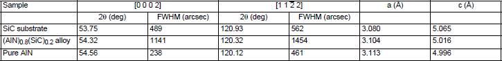

Figure 3. Pole figure of (a) symmetric (0002), and (b) asymmetric (11
A Raman spectrum recorded on the (0001) face of the AlN single crystal is presented in Figure 4. All the peaks can be assigned to AlN Raman modes: A1(LO)≈ 889cm−1 and E2(high) ≈ 655cm−1. The linewidth of E2 mode was as narrow as 9 cm−1 which also verified the high quality of our crystal Reference Kuball, Hayes, Shi and Edgar[18]. The AlN phonon frequencies point to a largely unstrained AlN crystal in agreement with XRD results Reference Kuball, Hayes, Prins, van Uden, Dunstan, Shi and Edgar[19], Reference Hayes, Kuball, Shi and Edgar[20].

Figure 4. Raman spectra of pure AlN single crystal.
4. Conclusions
Seeded bulk growth of a crack-free AlN single crystal was achieved on a SiC substrate by (1) depositing an AlN buffer layer on the SiC substrate by MOCVD below 1100°C, (2) forming an (AlN)x(SiC)1−x alloy film by condensing vapors sublimated (at temperatures above 1700°C) from a source mixture of AlN-SiC powders, followed by (3) condensing vapors sublimated from a pure AlN source. This method solves three problems previously associated with using SiC as seed crystals for AlN growth. First, the low temperature deposited AlN layer promotes layer-by-layer growth forming a continuous single grain. Second, the intermediate properties of the (AlN)x(SiC)1−x alloy reduces cracking in the growing crystal. Third, the presence of silicon and carbon in the source material reduces or eliminates the decomposition of the SiC substrate during sublimation crystal growth, enabling longer duration crystal growth. By employing this technique, a high quality AlN single crystal was produced as determined by Raman spectroscopy and X-ray diffraction. Such crystals are ideal for seeding AlN crystal growth at high temperature and hence high growth rates, to produce substrates for AlxGa1−xN based electronics.
ACKNOWLEDGMENTS
We are grateful for the support of this research from BMDO (Contract No: N00014-98-C-0407), ONR (Contract No. N00014-99-1-0104), and the Assistant Secretary for Energy Efficiency and Renewable Energy, Office of Transportation Technologies, as part of the High Temperature Materials Laboratory User Program, Oak Ridge National Laboratory, managed by UT-Battelle, LLC, for the U.S. Department of Energy under contract number DE-AC05-00OR22725. The work at the University of Bristol was supported by Renishaw plc, EPSRC, the Royal Society and British Council.


