Introduction
As the materials system of GaN grows into maturity all the usual problems associated with the influence of deep centers on electrical properties of GaN films become increasingly important. A number of groups have reported the results of studies of deep levels in n-GaN using deep levels transient spectroscopy (DLTS) and related techniques (a recent review and relevant references can be found e.g. in [Reference Polyakov and Pearton1]). At the same time there are many indications that nonradiative recombination via deep traps is an important recombination channel in GaN (see e.g. a review in [Reference Monemar2]). However, no attempt has been made so far to pinpoint the deep traps that play an important role in generation-recombination of charge carriers in GaN. In this paper we tried to establish such a correlation between the type and density of deep traps and the diffusion lengths in several n-GaN films widely differing by the diffusion length values.
Experimental
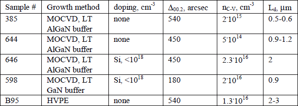
The samples studied in this paper were grown either by metalorganic chemical vapor deposition (MOCVD) technique or by hydride vapor pressure epitaxy (HVPE) on basal plane sapphire substrates. The details of growth can be found in [Reference Lundin, Pushnyi, Usikov, Gaevski, Baidakova and Sakharov3,Reference Melnik, Nikitina, Zubrilov, Sitnikova and Dmitriev4]. MOCVD samples varied from each other by the type of low temperature (LT) buffer (either GaN (sample 598 below) or AlGaN (samples 385, 644, 646 below)). Samples 598 and 646 were lightly Si doped, other samples were undoped. The thickness of all samples was 3−4 μm. Characterization included double crystal high resolution x-ray diffraction (HRXRD) measurements with Mo Kα source, capacitance-voltage (C-V) measurements on Au Schottky diodes with the diameter of about 1 mm, deep levels spectroscopy (DLTS) with electrical and optical injection and electron beam induced current (EBIC) profiles measurements at 300K. The latter profiles were used to extract the values of diffusion length of minority carriers. For persistent photocapacitance measurements a series of capacitance versus voltage and capacitance versus temperature (C-T) curves were measured at various frequencies before and after illumination at 85K with deuterium UV lamp and also with various light emitting diodes and with white light source equipped with selective filters. The Au Schottky diodes were prepared as described in [Reference Polyakov, Smirnov, Govorkov, Greve, Skowronski, Shin and Redwing5]. The details of experimental set-ups and measurement procedures can be found in [Reference Polyakov, Smirnov, Govorkov, Greve, Skowronski, Shin and Redwing5,Reference Polyakov, Smirnov, Usikov, Govorkov and Pushnyi6].
Results and Discussion
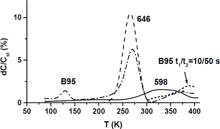
Table I presents the values of the (00.2) x-ray reflection halfwidths, Δ00.2, of room temperature electron concentration established from C-V measurements at 1 kHz (nC−V) and of diffusion lengths (Ld) in various n-GaN samples studied in this paper. It can be seen that the crystalline quality, as assessed by the halfwidth of the (00.2) reflection is the best for the MOCVD sample 598 grown on LT GaN buffer. The quality of the HVPE sample B95 and of the undoped MOCVD sample 385 grown using an LT AlGaN buffer is the worst in the same terms, while the undoped MOCVD LT AlGaN buffer sample 644 and lightly Si doped MOCVD LT AlGaN buffer sample 646 occupy the intermediate position. In search of centers responsible for the observed changes of Ld we first carried out DLTS with electrical injection measurements. DLTS studies on sample 385 have already been published in [Reference Polyakov, Smirnov, Usikov, Govorkov and Pushnyi6] (this is sample #1 of [Reference Polyakov, Smirnov, Usikov, Govorkov and Pushnyi6]). They showed the presence of only one dominant electron trap with apparent activation energy of 0.55 eV (the ET4 trap in the system of notation proposed in [Reference Polyakov and Pearton1]). The density of these traps was found to be 2.8.1015 cm−3. Figure 1 shows DLTS spectra measured for samples 646, B95 and 598 with time windows t1/t2=100 ms/1000 ms, with reverse bias of −0.5 V and the forward bias pulse of +1V ( the pulse duration was 2s).

Figure 1. DLTS spectra with electrical injection measured for samples 598, 646 and B95. Measurement conditions: reverse bias of −0.5V, forward bias of 1V (2 s duration), t1/t2=100/1000 ms (for sample B95 we also show the high temperature portion of the spectrum measured with t1/t2=10/50 s)
Table I. Electrical and structural properties of the studied samples
For sample 646 the only feature is the peak near 270K corresponding to the same ET4 trap as in sample 385. The concentration of this trap was 6.2.1015 cm−3. In sample B95, in addition to the ET4 trap with concentration 2.8.1015 cm−3, we observed an electron trap with activation energy 0.25 eV (the ET2 trap [Reference Polyakov and Pearton1]) with concentration 2.5.1014 cm−3, the electron trap with activation energy of 0.8 eV (the ET6 trap [Reference Polyakov and Pearton1]) with concentration of 6.4.1014 cm−3, and an electron trap with activation energy of 1 eV that is not well resolved for t1/t2 windows of 100/1000 ms but was clearly visible with longer windows of 10/50 s (the trap concentration was 9.3.1014 cm−3). In sample 598 we did not observe the ET4 traps in measurable concentrations. Instead one could observe a broad feature near 300−370K that is obviously a superposition of two or more peaks due to some unidentified electron traps ETX and a trap with activation energy of 1 eV reminding a similar center in sample B95 but having a higher capture cross section. The densities of corresponding traps were 8.1014 cm−3 (ETX) and 2.3.1014 cm−3(1 eV trap). Comparing the above results with the Ld values in Table I shows that none of the electron traps shallower than 1 eV can account for the observed changes of Ld in various samples. Hole traps can be accessed in Schottky diodes by DLTS with optical injection (ODLTS), although getting the absolute values of the densities of traps depends on one’s ability to fully recharge them. Figure 2 presents ODLTS spectra of samples B95, 598 and 646. In all these spectra the dominant feature is the peak near 300K (for the time windows t1/t2=100/1000 ms) corresponding to emission of holes from hole traps with the energy level Ev+0.9 eV. This trap was previously observed in various GaN samples (see [Reference Polyakov and Pearton1] for discussion and relevant references) and was associated with the deep acceptor participating in the donor-acceptor pairs transition giving rise to the yellow luminescence band (this is the H2 hole trap according to notation proposed in [Reference Polyakov and Pearton1]). The concentration of the H2 traps as deduced from the amplitude of the ODLTS peak was about 3.8.1014 cm−3 in sample B95 and close to 2.9.1015 cm−3 in samples 598 and 646. ODLTS measurements for sample 385 have been already published [Reference Polyakov, Smirnov, Usikov, Govorkov and Pushnyi6] and they showed no detectable signal from the H2 traps. Once again one has to conclude that these traps are not the ones responsible for recombination lifetimes in n-GaN. The origin of the broad band-like signal in ODLTS spectra in Figure 2 at low temperatures is most likely due to a band of relatively shallow states in the lower half of the bandgap. The nature of this band could be further elucidated by photocapacitance measurements at low temperature and by C-T measurements before and after illumination. These measurements were performed on samples 598, 646, B95. All the samples showed an onset of measurable photocapacitance near 1 eV (about 2 pF in sample 598 and much more pronounced in samples B95, 646), slight increase near 2.5 eV, no further growth for photon energies up to 3.1 eV and a very strong increase of capacitance upon above-bandgap illumination with the deuterium UV lamp. This increase of capacitance persisted after the UV light was switched off and could be either fully (in sample 598) or partially (samples B95, 646) removed by applying forward bias of higher than 0.8 V. That shows that the metastability in question is due to charging of deep traps located below the Fermi level. This trapped positive charge led to a decrease of the built-in voltage of the diodes Vbi after illumination (Vbi PPC) compared to the built-in voltage in the dark (Vbi). The difference, ΔVbi can be used to calculate the density of recharged traps Nt from the expression [Reference Berman and Lebedev7]:
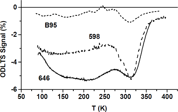
Figure 2. ODLTS spectra in samples B95, 598 and 646; measurements were made at −0.5V reverse bias, with a UV deuterium lamp injection pulse 2 s long; the spectra are shown for time windows t1/t2=100/1000 ms.
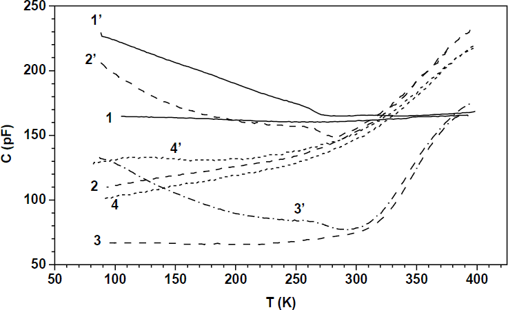
where w0 is the space charge region (SCR) width under illumination, q is the electron charge, ε0 is the permittivity of vacuum and ε is the relative permittivity. The results of these calculation are shown in Table II. It can be seen the density of traps is very high-on the order of some 1016 cm−3 in all the samples. Figure 3 shows how these metastable changes of capacitance decrease with temperature. In all three samples this happens in two stages: a broad step at 85K−250K and a step near 270K. The first of these steps is most probably due to a band of relatively shallow hole trap states in the lower part of the bandgap. The second step is definitely due to detrapping of holes from the H2 traps as was demonstrated by 1.3-eV-light optical quenching experiments to be reported elsewhere. We tentatively propose that the extended band of hole trapping states could be due to dislocations which is based on the extended nature of the states we observe and on the fact that the aggregate density of these states - some 1016 cm−3 - has the right order of magnitude for the dislocation density of ∼109 cm−2. The major difference between samples 598 and B95, 646 is that the latter ones show persistent increase of electron concentration after illumination while the former does not, as can be seen from shallow donor measurements by C-V in the dark (Nd) and after illumination (Nd PPC) (see Table II). This correlates very well with the absence in DLTS spectra of sample 598 electron traps ET4 which are present in samples 646 and B95 (see Figure 1). These traps have been shown to possess a barrier of about 0.15 eV for capture of electrons [Reference Polyakov, Smirnov, Usikov, Govorkov and Pushnyi6] and thus should lead to persistent photoconductivity at low temperature. C-T curve 4’ in Figure 3 shows that the step corresponding to capture of electrons by the ET4 trap ends near 200K which is fully compatible with the measured barrier height (the curve was obtained by illuminating B95 sample with UV light and filling all the centers but the ET4 traps with a forward bias pulse of 0.8 V; similar results were obtained by illuminating the sample with 1.3 eV light - the results of these experiments will be presented elsewhere).
Table II. Persistent photocapacitance results for various GaN samples


Figure 3. C-T curves for various GaN samples measured at 1 kHz when cooling in the dark (1, 2, 3, 4) and after illumination with the deuterium UV lamp at 85K (1’, 2’, 3’, 4’). Curves 1, 1’ are for sample 598, 2, 2’ for sample B95, 3, 3’ for sample 646. Also shown are the cooling down and heat-up curves for sample B95 illuminated with UV light and quenched with forward bias pulse of 0.8 V (curves 4, 4’; note that only the signal from PPC due to ET4 trap can be seen).
If the situation with persistent photoconductivity (PPC) is reasonably well understood in our samples the nature of the recombination channel competing with radiative recombination remains elusive. None of the centers described above can aspire to such a role. Perhaps surface recombination could be held responsible here but this question obviously requires further study. It also remains to be seen whether the band-like states near the valence band detected in our ODLTS and photocapacitance measurements could play any significant role in recombination. These states undoubtedly can capture electrons at a certain rate as demonstrated by forward bias pulse filling experiments but the total density of states in the band seems to be almost the same in samples with significantly different Ld values. To us it seems more likely that these band states are rather hole traps and compensation centers. If indeed the states are associated with dislocations they could contribute to forming the barriers for recombination around dislocations and explain lowered radiative recombination efficiency near individual dislocations demonstrated recently by several groups (see an extensive discussion and relevant references in [Reference Polyakov and Pearton1]).
Conclusions
We have shown that in n-GaN there exist band-like states in the lower portion of the bandgap. These states have the total density of some 1016 cm−3 and can give rise to very large metastable changes of capacitance at low temperatures.
Persistent photoconductivity in n-GaN films is associated in part with the ET4 electron traps having a relatively high barrier for capture of electrons.
In n-GaN there exist unidentified recombination channels that effectively compete with the radiative recombination transitions. But none of the centers detected by capacitance spectroscopy can be associated with such channels.