


Introduction
Over the past fifty years, lasers have found many applications in science and technology. The most important features of lasers are that photons are inherently free of elemental contamination, extremely high-energy densities can be focused to small diameters, and the laser beam can be precisely positioned using deflection mirrors. By reducing pulse lengths from a few nanoseconds down to the picosecond or femtosecond range, superficial surface heat damage from ablation can be reduced to depths of a few microns or less. Available for many decades, lasers have become extremely reliable processing tools in many areas, including the automotive industry (welding, drilling, and measuring), thin-film processing (scribing, patterning), and even esthetic surgery (dermabrasive ablation, LASIK).
In view of the outstanding characteristics of lasers as tools for micro machining, it is surprising that instruments for specimen preparation, for state-of-the-art analytical techniques, have not made use of laser technology. 3D-Micromac company has developed a dedicated laser micromachining instrument for specimen preparation. The name of this instrument indicates its purpose: microPREP (microscopy preparation) (Figure 1).
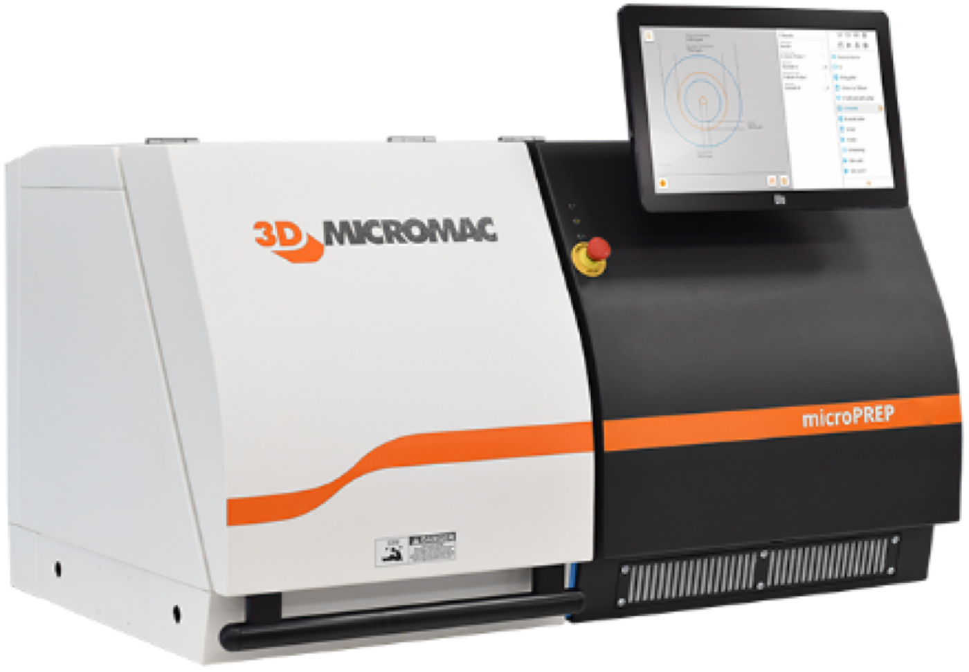
Figure 1: The 3D-Micromac microPREP, a laser-based specimen preparation system.
At sufficiently high power (or more precisely fluence), laser radiation is able to ablate all kinds of materials. Using ultra-short pulses and high pulse energies, ablation-based tools can also process materials that are transparent to the laser’s wavelength. The ablation rate of laser micromachining is about six orders of magnitude larger than that of the Ga-ion beam used in focused ion beam (FIB) workstations, and it is even about four orders of magnitude higher than the milling rate of the Xe-plasma-FIB. Moreover, lasers can be very precisely positioned on a given workpiece and straightforwardly focused using standard optical elements. Since laser radiation consists just of photons (rather than an ion beam, which may have unwanted implantation effects), laser micro-machining is clean in terms of contamination. This article shows how this technology can be used to produce thin lamellae for transmission electron microscopy (TEM) and sharp tips for atom probe tomography (APT) [Reference Sato and Byrnes1–3].
Materials Methods
Tasks for the laser
Specimen preparation techniques need to be fast, reliable, cost-effective, and artifact-free on the micrometer scale or smaller. Traditional mechanical specimen preparation and FIB systems currently dominate the field. While the former is accompanied by the high costs of time-consuming processes, the latter is characterized by the high costs of instrument ownership.
There are a number of specific capabilities of a laser-based thin-specimen preparation tool. Based on several patents [e.g., Reference Höche4,Reference Krause and Höche5], the tool described here has a range of basic functionalities, including laser cutting from the bulk, followed by local laser thinning in an almost entirely automated fashion. Making use of a rugged, ultra-short-pulsed laser source, the process is characterized by low running costs, suitability for all materials of modern microelectronics, freedom from contamination, and a precision of about one micrometer.
Instrumental setup and performance
The main components of the microPREP instrument are a 532 nm laser source with 3 W average power and an objective lens focusing the laser beam to a small probe (beam diameter ∼10 µm). The pulse energy of up to 60 μJ enables high ablation rates compared with a broad Ar+ ion beam or the focused Ga+ or Xe+ ion beams used in FIB instruments. Figure 2 shows a (300 × 300 × 250) μm3 box milled by using the microPREP instrument. This specific preparation was done in less than 5 min. If a FIB were used for the same task, it would take up to 17 days. Thus the removal of bulk material can be efficiently done by means of this laser instrument, but the speed still depends on the dimensions, the task, and the specific material to be removed.
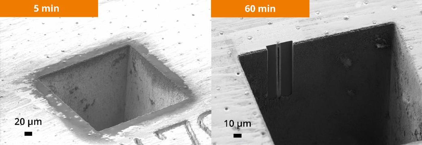
Figure 2: Boxmilling. (left) A Si sample (300 × 300 × 250 μm3) machined by microPREP in 5 minutes. (right) Excavated through silicon via (TSV) in the box prepared by the microPREP and finished using a Zeiss Auriga 40 FIB.
Heat-affected zone
Widespread use of laser micromachining for the preparation of thin TEM specimens has been hampered by concerns regarding thermal damage to the sample. It is important to note that this effect can be controlled and minimized, depending on the material and the analysis task. The formation of a melt takes place when traditional pulsed laser (not ultra-short-pulsed) radiation interacts with matter and expels material from the location of machining. This heating is caused by the electromagnetic wave from the laser, which excites phonons and leads to a local increase in temperature.
For ultra-short pulsed lasers, however, the excitation is absorbed by the electronic system of the material, leading to much reduced heating effects. Ablation is not entirely “athermic,” but it was found to be restricted to a depth of less than 0.4 µm for silicon [Reference Höche6–Reference Martens9]. The extent of this heat-affected zone (HAZ) can become larger when basic principles of laser micromachining are not obeyed, for example, when the feed rate is too slow. Nevertheless, there is still a layer of material, micrometers in extent (worst case), which will sustain some structural damage. This structural damage strongly depends on the given material and the laser parameters used. To keep structural damage small and under control, the ablation process is restricted to a highly localized area. The HAZ is entirely removed by the FIB process. Depending on the material, the specific specimen, and the FIB parameters themselves, it can take few seconds to few minutes to remove the HAZ.
Workflows
Different workflows have been developed for processing bulk samples, cross sections, tomography, atom-probe pillars, and samples for micromechanical testing. Specimens for TEM and APT generally have starting dimensions of 1–3 mm. The workflow for cross-section preparation in the “XL-Chunk” mode is described below and shown in Figure 3.
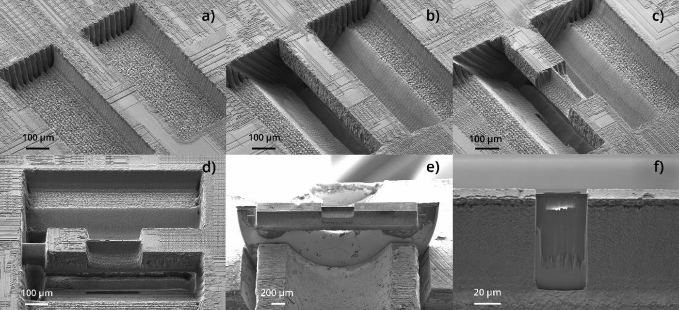
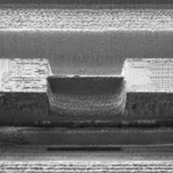
Figure 3: Workflow for cross-section preparation in the XL-Chunk mode. (a) Laser milling of two side-boxes, which are required for the second step and for ease in handling with tweezers. (b) Laser milling of trenches/undercut, which will allow freeing the sample from the rest of the bulk material. (c) Laser cutting or milling of the required structures (H-bar, or pillars/tips). (d) Laser cutting of support structures. (e) SEM micrograph of the laser-machined XL-Chunk with local thinned area glued to a half-ring. (f) SEM micrograph of a structure in silicon after local thinning (post-processing) with the laser and a FIB. (a–d) were taken by the microPREP overview camera. (e–f) were taken with the SEM of a Zeiss Auriga 40.
The following cross-section workflow, based on the XL-Chunk approach, consists of five steps: (1) Laser milling of trenches/undercut, which will allow freeing the sample from the rest of the bulk material. (2) Laser cutting or milling of the required structures (H-bar, or pillars/tips). (3) Laser cutting of support structures. (4) Removal of workpiece and gluing to a copper half-ring. (5) Post-processing with an Ar+ ion broad beam or with a focused Ga+ or Xe+ ion beam to remove structural damage in the HAZ.
This XL-Chunk workflow can be applied for TEM lamellae. Atom probe pillars can be prepared in two ways. One approach of a direct preparation of the pillar/tip on top of the XL-Chunk is shown in Figure 4. This illustrates that ultra-short-pulsed lasers are capable of fabricating tiny pillars in an automated fashion, which can be used as mounts or basic structures for APT.
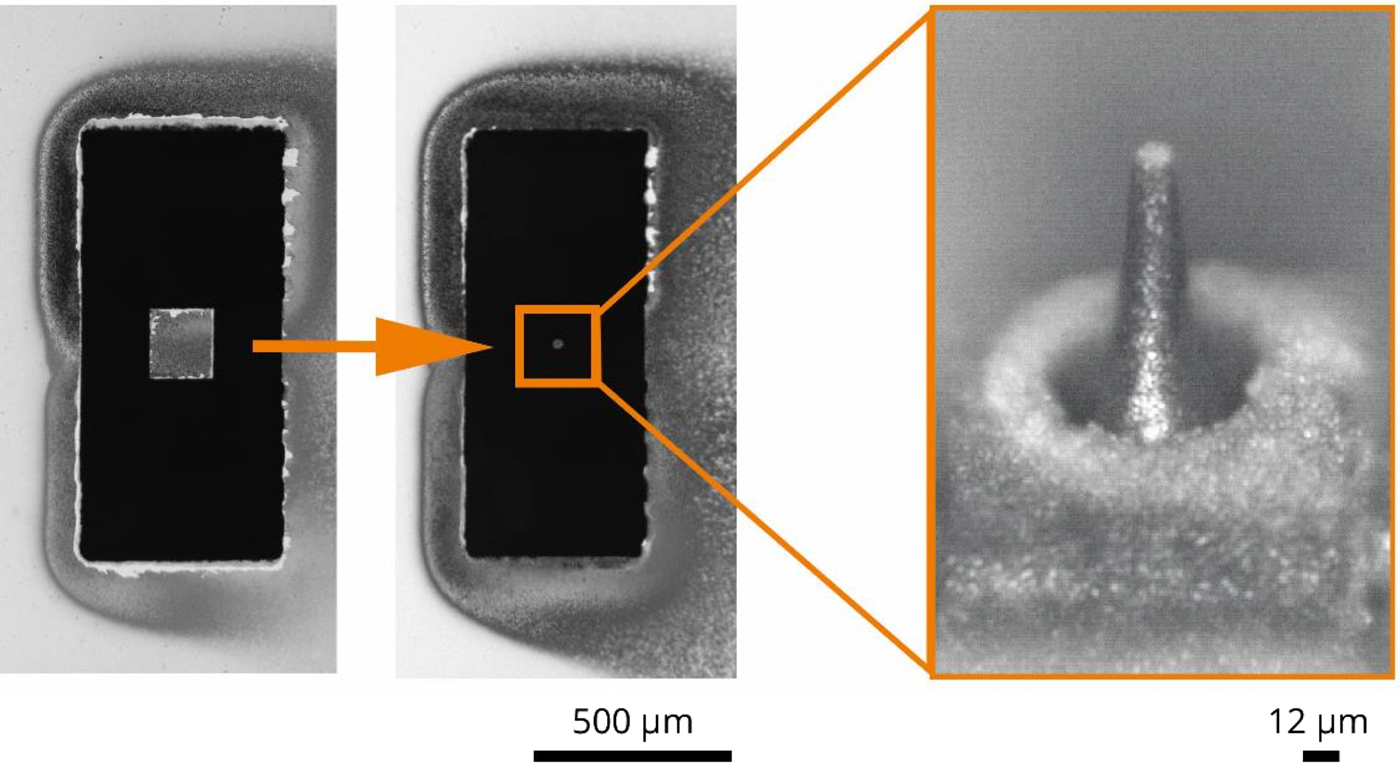
Figure 4: APT pillar preparation in silicon based on the XL-Chunk workflow. The pictures were taken by the microPREP overview camera.
Figure 5 shows a variety of forms and tasks that have been produced with this instrument for different methods of analysis. Another feature is the capability to upload CAD files. With this feature, regions of interest can be investigated by means of computer-aided navigation on the specimen, which is especially useful for semiconductor devices. Most tasks to be accomplished in this way involve quality assurance, failure analysis, or random sampling.
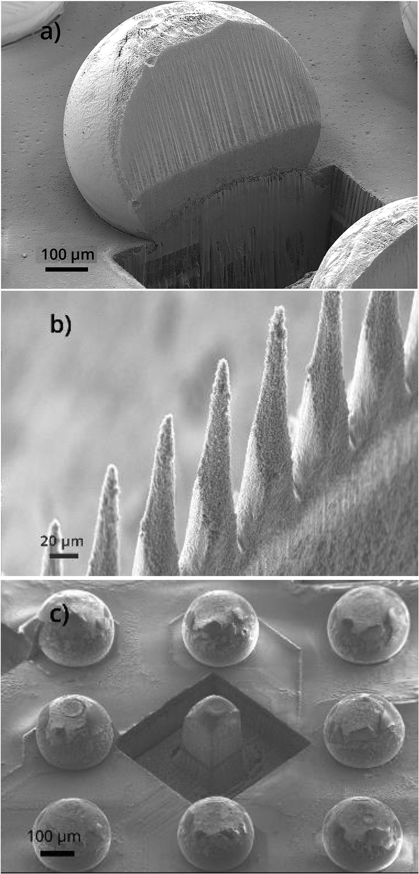
Figure 5: Examples of different preparation tasks showing the free form capability of the microPREP. (5a) Bump of lead-free solder SAC 305. (5b) Silicon APT samples. (5c) Ball grid array of lead-free solder SAC 305 bumps. SEM images taken with Carl Zeiss Supra55VP.
Cleaning
The aforementioned steps 1–5 for XL-Chunk preparation are done under ambient conditions without vacuum or inert gas atmosphere. Nevertheless, for the best results in terms of specimen cleanliness and an optimal start for post-processing steps, the instrument can be fitted with a contactless cleaning system called CO2 Snow Jet. This comprises a source of liquid CO2, a pressure reducer, a gas flow control unit, and a cleaning nozzle. After each processing step it is possible to add a cleaning step. The CO2 is inert to the specimen and can be applied without concerns regarding contamination or unwanted implantation effects. Figure 6 shows a specimen before and after snow jetting. The debris is broadly removed without interfering with the specimen.
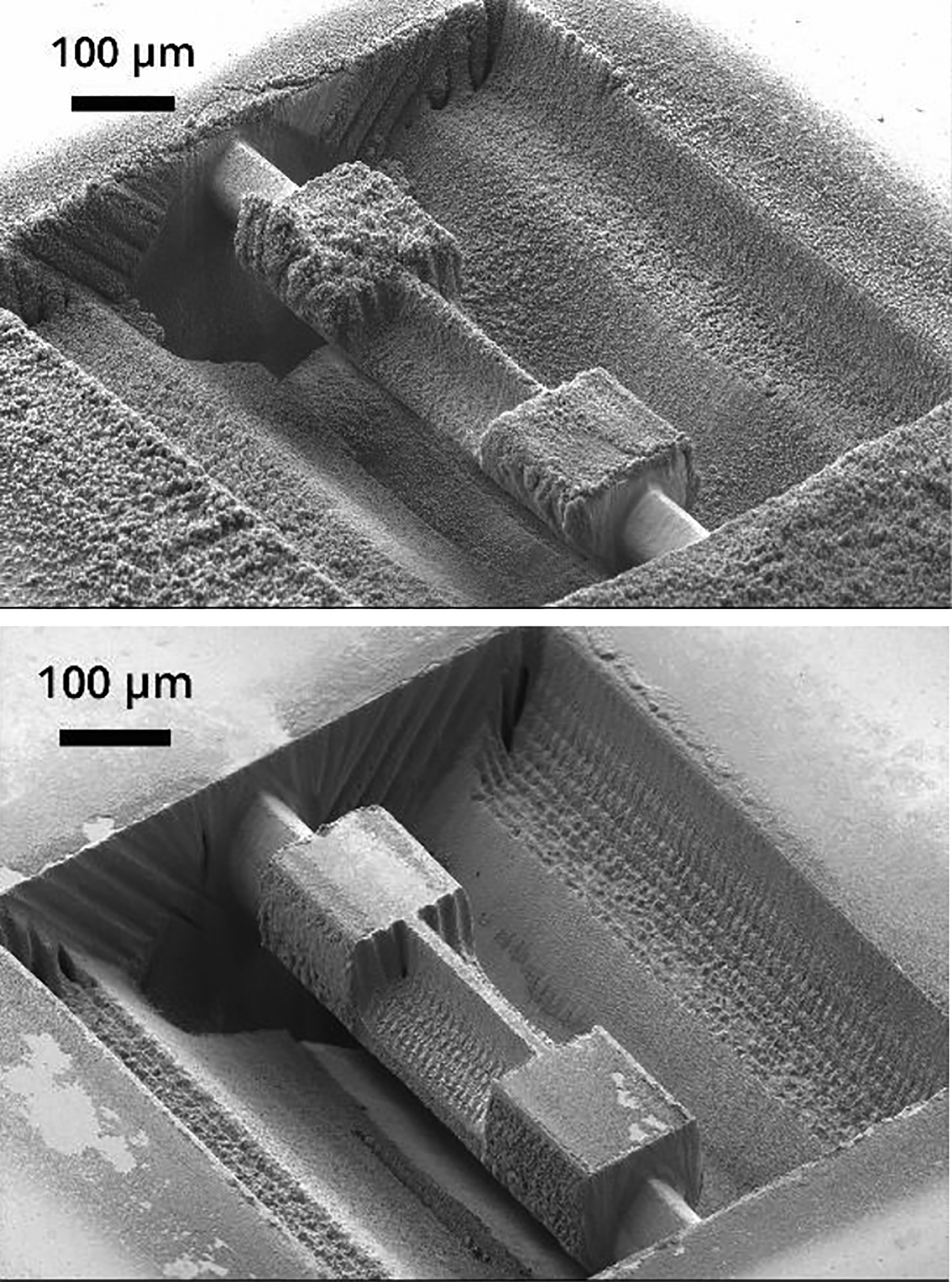
Figure 6: Specimen cleaning. (top) Specimen after laser processing without cleaning. (bottom) Specimen after processing and cleaning with CO2 Snow Jet. This specimen was machined by microPREP only, without additional FIB polishing.
Flexibility
The laser is a high-energy light with a final beam diameter of about 10 µm, which is directed by a precise laser scanner. The sample is held by a precise stage system (up to 6 axes), in order to position the region of interest in the center of the scan field. Thus, sample geometries like tips, bars, or other geometrical patterns can be machined from almost any type of material. Electron transparent sections can be made at one position or at multiple positions. In addition, multiple workflows allow the preparation of samples at several different, pre-determined positions, enabling automated high-throughput sample preparation. This mode is particularly valuable for metrology, evaluation of homogeneity, and screening applications.
Results
Laser micromachining of H-bars in IC-structures
An XL-chunk was prepared from an IC-structure while keeping supporting structures in place until the workpiece was removed with tweezers. In order to observe the structure in a TEM, the thinned region was glued to a 3 mm copper half-ring (Figure 3e). In the next step, a FIB system was used to remove the HAZ and to thin the sample to the required thickness of < 100 nm (Figure 3f). The effectiveness of the instrument can be shown by milling a box (300 × 300 × 250) μm3 in silicon material within 5 minutes and the post-processing with a FIB (Figure 2). Figure 5 shows different preparation tasks and some free-form capabilities. Figure 6 shows the contactless nonabrasive cleaning using the CO2 Snow Jet.
Discussion
The XL-Chunk design is a support structure to hold TEM lamellae or atom probe tips. For APT, it is also possible to prepare several tips, as a line or an array of tips. It is also possible to mill complete APT cards. Modular design and flexible software allow the integration of this new type of chunk specimen prep into other workflows. Laser processing is an effective method for rapidly removing significant volumes of material to reduce the total time to a finished specimen. Since CO2 cleaning is nonabrasive, it is a useful process for removing redeposited material. Further developments are ongoing to reduce the HAZ and also to expose samples to a defined micro-environment (inert gas or vacuum) to minimize oxidation.
Conclusions
A new ultra-short-pulsed laser-based thin specimen preparation system provides fast, cost-effective, and site-specific preparation of samples for microstructure evaluation. The microPREP is not just a tool to prepare thin samples for TEM, it also can prepare specimens for APT and micromechanical testing. The modular stage and software design of the microPREP laser tool meets the exacting requirements of several industries.
Acknowledgments
The work presented in this paper has been performed in the project SAM3. The German partners are funded by the BMBF (German Federal Ministry of Education and Research) under contract 16ES0347, and the French partners are funded by the French Ministry for Industry and Economy. SAM3 is a joint project running in the European EUREKA EURIPIDES and CATRENE programs. We would like to thank all our partners in the aforementioned project.


