


Introduction
The development of large-area silicon drift detectors (SDDs) provides a significant improvement in X-ray micro-analysis, especially in scanning electron microscopes (SEMs) and electron microprobes, where high incident probe currents are possible. The resultant improved detection limits and/or speed of elemental mapping and analysis make the SDD the detector of choice for microanalysis [Reference Newbury1]. With the larger geometric collection efficiency and faster response times of these detectors, the higher input count rates can place significant demands on the performance and speed of the signal processing electronics.
There are numerous benefits of using SDD technology for X-ray microanalysis when compared with conventional Si(Li) detectors, including:
1) larger geometric collection efficiency as a result of the much larger detector area that is possible without loss of energy resolution
2) higher count rate capability (300–800 kc/s) from the lower capacitance of the SDD versus conventional Si(Li) detectors
3) the possibility of improved energy resolution (some detectors offer ~125 eV)
4) no liquid nitrogen cooling required (thermoelectric cooler with passive or active secondary cooling) and rapid cool down to operating temperature (~30 minutes)
5) light weight (relates to column stability) and physical size (low acoustic interaction) of the SDD in part as a result of the elimination of the liquid nitrogen dewar
One drawback of the SDD is the thinner active volume (450 mm for the detector being discussed compared to the nominal 3-mm thickness of most Si(Li) crystals). This results in a decreased detection efficiency for X-rays with energies >10 keV because a greater fraction of such X-rays pass through the SDD. There could, however, be an advantage in using the thinner SDDs for microanalysis of radioactive materials that emit high-energy gamma rays as they decay. These gamma rays cause higher background counts , detector reset rates, and attendant higher dead time for conventional (that is, thicker) Si(Li) detectors. Gamma rays would deposit less energy into the thinner SDD detector, possibly with reduced deleterious effects on microanalysis.
The performance of the present SDD on a JEOL 6500F SEM will be discussed here as a function of detector time constant (TC) and input count rate [Reference Kenik2, Reference Kenik3]. The stability of energy resolution and peak energy will be addressed along with pulse pile-up effects, including sum peaks and energy tailing.
Materials and Methods
The detector was mounted on one of the standard EDS ports of a JEOL 6500F SEM (Figure 1). The JEOL 6500F SEM was designed with a high-brightness Schottky field emission gun (FEG) that is placed in the magnetic field of the first condenser lens. This design provides high beam currents (up to 200 nA for some conditions) at small probe diameters. Data collection and analyses were performed using a commercial X-ray microanalysis system with a digital pulse processor, which is designed for improved pulse processing and signal discrimination. The SDD is an older style 40-mm2 Ketek chip with a 30-mm2 aperture to collimate the X-rays to the center of the chip. This chip has been replaced by newer chips in currently available SDDs. The detector system manufacturer indicates that this design results in spectra with improved peak-to-background ratio (P/B). The SDD is cooled to –60ºC by a double stack of Peltier thermoelectric coolers, which are subsequently cooled by an external, non-aqueous chiller. In general, spectra were acquired at 20 kV and 100-second clock time (unless otherwise specified). A pure manganese elemental standard was used for many of the performance tests. Calibration of the absorbed specimen current for this Mn standard versus the incident probe current was performed with a Faraday cup and a Keithley 6485 picoammeter.

Figure 1: Silicon drift detector mounted on a JEOL 6500F SEM. Note the plastic lines on the left back of the detector for non-aqueous cooling of the Peltier thermoelectric cooler stack.
A brief definition of some of the terms used in this paper is included to avoid confusion. The input count rate is the number of electronic pulses per second that are sent to the detector electronics. The input count rate quoted in this paper is that indicated by the software package during spectrum acquisition. In general, each pulse should represent a single X-ray detected. The throughput, or throughput count rate, is associated with the pulses (X-rays) that are successfully processed by the detector electronics and placed in the acquired spectrum.
Results
The SDD provides ~3.5× the geometric collection of the previous conventional 10-mm2 Si(Li) detector. As the SDD has a 3× larger active area relative to that of the nominal 10-mm2 Si(Li) detector, the observed ~3.5× increase may be due to small differences in the actual active areas of the two detectors or to slightly different detector-to-specimen distances. The fast time constants that are permissible because of the low capacitance of the SDD allow spectra to be collected at high input count rates (as high as ~500 kcps). Spectra acquired for the Mn standard at ~22 percent dead time (DT) for six different time constants (0.5–12.8 ms) are compared in Figure 2. In addition to the Mn-Ka, b, and Mn-L peaks, there are spectral artifacts that appear at high count rates and short time constants, such as peak shifts, peak broadening associated with a loss of energy resolution, high-energy tailing (for example, above the Mn–Ka peak), sum peaks (for example, the 2× peaks near 12 keV), and other pulse pile-up effects. It should be noted that the sum peaks become progressively non-Gaussian in shape for shorter time constants. There is a decreased intensity of low-energy X-rays below the Mn L peak, especially at the two fastest time constants. Because the spectra are normalized (Mn Ka to 4× full scale), there is a slight increase in the background at higher input count rates associated with a loss of Mn Ka intensity due to pulse pile-up.
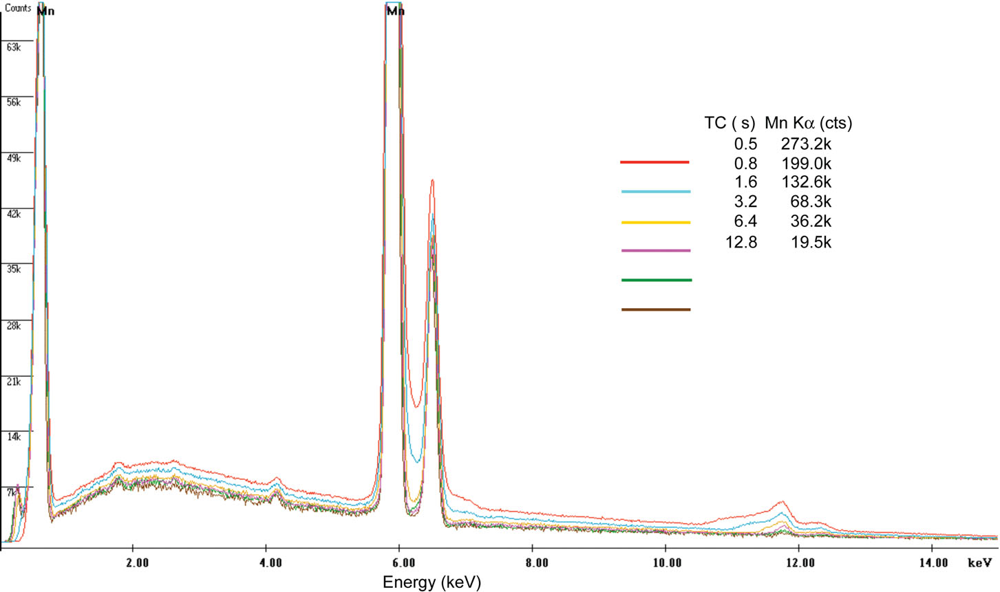
Figure 2: Spectra of the Mn standard as a function of time constant (TC) at 20 kV and ~22-percent DT. The Mn Ka peaks are normalized to 4× full scale. Net counts are given for the Mn Ka peak for 100 clock second acquisition.
Input count rate capability, throughput counts, energy resolution/stability, energy stability, and spectral artifacts (sum peaks and peak broadening) all impact the quality and quantification of X-ray microanalysis. As such, performance testing is required to identify the operational space for both the detector and the processing electronics that yield spectra of sufficient quality for valid analyses.
The throughput for the Mn standard as a function of indicated input count rate and time constant is shown in Figure 3. It should be noted that the maximum throughput occurs at progressively lower dead times for faster time constants (higher input count rates). The maximum throughputs observed occur at 61, 61, 61, 57, 53, and 49 percent dead time with progressively shorter time constants (that is, 12.8, 6.4, 3.2, 1.6, 0.8, and 0.5 ms, respectively). If the detector and processing electronics are processing pulses in an optimized fashion, the maximum throughput should occur at a calculated dead time of ~65 percent [Reference Anderhalt4]. It is presumed that these lower dead time values for maximum throughput are related to either the increased fraction of detector live time lost to detector reset events or to processing electronics problems associated with the high input count rates.

Figure 3: Throughput for the Mn standard as a function of indicated input count rate and time constant at 20 kV. Note that the maximum throughput occurs at progressively lower dead times for faster time constants (see text).
A second problem noted in Figure 3 is the saturation of input count rate for the 0.5-ms time constant at ~500 kcps, even though the last data point was taken with ~24 percent higher probe current than the penultimate data point. The detection of this effect required the high incident probe currents (~100 nA at 20 kV) that the JEOL 6500F SEM was able to provide. As indicated previously, the input count rate is that indicated by the software package during spectrum acquisition. This result is an obvious indication of a non-linearity between indicated input count rate and incident probe current, which will be discussed later.
Typical spectra from the Mn standard for the 1.6-ms time constant as a function of indicated input count rate are presented in Figure 4. In a fashion similar to the effect of shorter time constants shown in Figure 2, increased input count rate at the same time constant results in increased spectral artifacts (peak shift, peak broadening, high-energy tailing, sum peaks, and other pulse pile-up effects). An additional effect is the indication of apparent X-rays at higher energies than the energy of the incident electrons, which is a physical impossibility but reflects the increased probability of pulse pile-up at high count rates.
Figure 4: Spectra for the Mn standard measured at 20 kV for the 1.6-ms time constant as a function of indicated input count rate.
The energy resolution of the Mn Ka peak as a function of time constant and input count rate is given in Figure 5. As would be expected, the best possible energy resolution (that is, smallest full-width at half-maximum [FWHM] at low count rate) improves as the time constant decreases. For the four slower time constants (that is, 1.6–12.8 ms), the FWHM is relatively constant (≤10-eV increase) as a function of input count rate over the entire range of usable count rates (<70 percent dead time). Though the increase in FWHM as a function of count rate is larger for the fastest two time constants, it remains relatively constant (≤10-eV increase) for input count rates less than ~275 kcps. It should be noted that the last four data points for the 0.5- and 0.8-ms time constants were collected at significantly higher dead time (DT) values than that for maximum throughput. Such non-optimized counting conditions normally would not be employed for actual X-ray microanalysis. Similar behavior is observed for the FWHM of the Mn L line, with slightly wider peaks resulting from the presence of multiple, unresolved L lines.

Figure 5: Energy resolution (FWHM) of the Mn Ka peak measured at 20 kV as a function of time constant and input count rate. It should be remembered that the 40-mm2 chip is an older Ketek chip that has been replaced by newer chips in currently available SDDs.
The displayed energy of X-ray peaks generally shifts to a slightly higher energy as a function of input count rate (Figure 6). The dominant origin of this shift is the assymetric broadening or high-energy tailing of the peaks at higher count rates (for example, see Figure 2). The slight variation in indicated peak energy at a low count rate for the different time constants simply reflects small differences in energy calibration. The apparent increase in peak energy for the four slower time constants (that is, 1.6–12.8 ms) is ≤10 eV as a function of input count rate over the entire range of usable count rates (<70-percent dead time). For the 0.5- and 0.8-ms time constants, the energy shift is ≤10 eV if the dead time is kept below ~54 percent (input count rates of 425 and 310 kcps, respectively), which would keep the input count rate at or below that for maximum throughout.

Figure 6: Apparent energy of Mn Ka peak as a function of time constant and input count rate.
The software offers a post-acquisition routine for removal of pulse pile-up effects. Figure 7 shows the result for a spectrum collected with the 3.2-ms time constant at 40-percent dead time before and after running the correction routine. Though the correction partially removes some pile-up effects (sum peaks, higher background between and above the Mn Ka and Kb peaks), it does not completely remove the sum peaks. The best correction removes ~60 percent (Figure 7) at 3.2-ms TC, 40-percent DT. For many other SEM and SDD operating conditions, the correction routine removes 40–50 percent of sum peaks. The correction routine removes more of the Ka peak than the Kb peak and does so asymmetrically. The correction routine [Reference Elam, Anderhalt, Sandborg, Nicolosi and Redfern5] is based on the earlier work of Wielopolski & Gardner [Reference Gardner and Wielopolski6], Statham [Reference Statham7], and Bristow and Harrison [Reference Bristow and Harrison8]. In his paper, Elam indicates that the spectrum correction requires “a realistic model of the hardware response,” which apparently is somewhat lacking for the current SDD. In addition, the correction sub-routine deletes the counts in the sum peaks and other pulse pile-up effects but does not return them to their correct (original) energies, as would be desired.

Figure 7: Spectrum for Mn collected with the 3.2-ms time constant at 40-percent DT and pulse pile-up corrected spectrum calculated by correction routine.
In order to understand the apparent non-linearity between input count rate and specimen current, as indicated by the saturation of the indicated input rate (Figure 3), the count rate was measured as a function of probe current, which was measured using a Faraday cup and picoammeter (the results for the 0.5-ms time constant are shown in Figure 8). The software package offers two measures of the input count rate. The first is displayed during spectrum acquisition, and the second is calculated after spectrum acquisition using a ratemeter function for the entire spectrum (0–40 keV for spectra collected at 20 keV in order to capture the counts at >20 keV resulting from pulse pile-up effects). Both of these rates are non-linear as a function of probe current, indicating a problem with the “fast channel” of the detector/pulse processing electronics that are used to determine the input count rate. If the true input count rate is estimated by linear extrapolation of the low count rate data as a function of probe current, the result is the straight line shown in Figure 8. The non-linearity probably starts below 200 kcps and becomes more pronounced at higher count rates. (The actual count rate is underestimated by a factor of ~3 at 100 nA (~500 kcps, ~75 percent dead time)). The results from the other time constants basically overlay the 0.5-ms data. The manufacturer agrees that this effect is present in the current generation of detector/processing electronics and processing software and will be addressed in the next generation of electronics hardware that should be available in the near future.

Figure 8: Input count rate for Mn standard at 20 kV as a function of incident probe current. Indicated and calculated values are input count rate displayed during acquisition and that calculated from a ratemeter function after the acquisition, respectively.
Because the indicated count rate saturates at 500 kcps for pure manganese at 20 keV, the true count rate is drastically underestimated as the saturation point is reached or exceeded. When conducting performance tests on other materials and other accelerating voltages, it became clear that the saturation point for the indicated input count rate depended on the average X-ray energy being processed. In contrast to manganese at 20 kV, a 50-percent higher saturation value for the count rate was measured for aluminum at 10 keV, indicating that the problem may be related to processing larger (and therefore longer) current pulses from the SDD.
To demonstrate the efficacy of the SDD in X-ray micro-analysis, elemental mapping of the fine-scale microstructure of a CMSX4 superalloy was performed by spectrum imaging at both 15 and 5 kV (top and bottom rows in Figure 9, respectively). The BSE images and corresponding X-ray maps shown in Figure 9 (100 × 128 pixels) reveal the primary and secondary g' phase (appears dark in BSE images) surrounded by g phase (appears bright in BSE images). The X-ray maps reveal the relative elemental distribution of Al, Cr, and Re for the two phases. The maps were acquired at either condition (1) 15 kV, 8 nA, 183-kc/s input, in ~9.6 min at 1.6 ms TC, 50-percent DT or condition (2) 5 kV, 6.8 nA, 60-kc/s input, in 8.6 min at 1.6 ms TC, 19-percent DT. It should be pointed out that for the 5-kV Cr elemental map, the Cr L peak, rather than the Cr K peak, was used. As would be expected, the spatial resolution of the maps is significantly improved for the 5-kV accelerating voltage as a result of the decrease in the excited volume. This is evident when compared with the increased “blurring” observed in the 15-kV elemental maps of the finely intermixed g′ + g areas (for example, Al, Cr, and Re maps).

Figure 9: BSE image and elemental maps (100 × 128 pixels) for Al, Cr, and Re from CMSX4 superalloy specimen at 15 and 5 kV (top and bottom row, respectively). See text for experimental details.
It is evident that the combination of the high-brightness FEG of the JEOL 6500F SEM, together with the high collection efficiency and high count rate capability of the SDD permits elemental mapping to be performed at speeds where instrumental problems such as specimen image drift do not degrade the spatial resolution, even at lower accelerating voltages where the reduced excited volume gives improved spatial resolution (the estimated lateral spatial resolution for the elemental maps is ~100 nm at 5 kV).
Discussion
The silicon drift detector (SDD) tested here provides both high geometric collection efficiency and high count rate capability for X-ray microanalysis and elemental mapping (spectrum imaging). Testing of this SDD on the JEOL 6500F SEM indicated input count rates ≥500 kc/s for a pure manganese standard. Pulse pile-up effects increased with increasing input count rate and decreasing time constant (which allowed higher count rates). However, it should be noted that the use of a pure Mn standard (or likewise another pure element specimen) is a stringent test for pulse pile-up effects as ~60 percent of the X-rays detected are in the Mn K and Mn L peaks (46 percent K, L 12 percent L). The intensity of a sum peak is proportional to the count rate for the two peaks being summed. For a given input count rate and specimens with multiple elements present, the total counts are divided among more peaks. This reduces the count rate for each of the peaks, thereby reducing the intensity of the sum peaks. Of course, there will be additional sum peaks from the multiple elements.
Both the energy resolution and peak energy increased slightly with input count rate. However, if the analyst uses optimized counting conditions (that is, input counts rates giving less than or equal to the maximum throughput), the increase in FWHM or peak position will be ≤10 eV, respectively. With the current generation of detector/processing electronics, there is a measurable degradation in the energy resolution as the time constant is decreased. It appears that the larger SDD chip is more prone to such effects, but no detailed testing of other SDDs with smaller active areas was undertaken as part of this work.
The throughput depends on time constant; a maximum throughput of ~215 kc/s is achieved at 0.5-ms TC. The DT at maximum throughput decreases at short TCs (~49-percent DT at 0.5-ms TC versus ~61-percent DT at 3.2- to 12.8-ms TC). The indicated input count rate saturates at high probe currents (~80 nA) and saturation depends on the average detected X-ray energy (for example, ~500 kc/s for Mn at 20 kV versus >750 kc/s for Al at 10 kV). Additionally, the indicated input count rate is not proportional to the probe current at high input count rates. It appears that the throughput and indicated input count rate problems are related to problems in the detector and/or processing electronics. Though the manufacturer is aware of these problems and is currently working on their next generation of signal processing electronics, a prototype was not available for testing at the time of writing.
Though the manufacturer has incorporated a routine for correcting pulse pile-up effects into their latest version of software, that routine does not appear to be correctly optimized for this large SDD (best case removal was ~60 percent of the counts in the 2× sum peak). The remaining sum peak was not symmetric. The current routine simply deletes the counts arising from pulse pile-up effects. Ideally the pile-up counts should be returned to their correct (original) energy.
Conclusion
From the results presented above, it is clear that there are numerous advantages of silicon drift detectors (SDDs) for SEM-based microanalysis and elemental mapping. The larger geometric collection effiency, high count rate, and high throughput capabilities and operation without liquid nitrogen offer benefits to the analyst. Peak shift with increasing input is minimal for usable input count rates (that is, <70-percent DT). As the detector using an older, large diameter SDD chip, the energy resolution does not match more current SDDs that can resolve <130 eV under optimum conditions.
Acknowledgments
Research was supported by the Oak Ridge National Laboratory's SHaRE User Facility, which is sponsored by the Scientific User Facilities Division, Office of Basic Energy Sciences, U.S. Department of Energy.


