


Introduction
Metal–insulator–metal (MIM) resonant absorbers have application to infrared (IR) sensing. The important long-wave-infrared (LWIR) spectral range is easily served by structures that can be fabricated by ordinary contact photolithography. Different types of absorbers would be of interest. Ones that span the 8–12 µm LWIR would be suitable for standard night vision applications. Ones that absorb narrowly within this band have application to spectral sensing. MIM LWIR absorbers have been applied to IR bolometers[Reference Smith, Nath, Ginn, Peale and Shelton1] and to pyroelectric detectors.[Reference Gokhale, Myers and Rais-Zadeh2]
MIMs that absorb in the 3–5 µm mid-wave-infrared (MWIR) band would be useful for, e.g., tracking very hot objects. This region requires very small metal patterns that are at the limit of what can be achieved by contact photolithography. The fabrication challenge is relaxed by choosing a dielectric with a low index.
Several of the coauthors recently published[Reference Nath, Modak, Rezadad, Panjwani, Rezaie, Cleary and Peale3] a comprehensive study of MIM absorbers at 50 µm wavelength in the far-IR spectral region, where the dispersion of the insulator used (SiO2) was weak. The resulting resonant absorption spectrum was simple and accurately agreed with the analytic standing-wave model introduced in that paper. This paper investigates MIM absorbers designed for MWIR, where dispersion is also weak for nearly all common dielectrics, and for LWIR, where dispersion can be strong. The main theme of this paper is the effect of that dispersion, which should inform the materials choice for MIMs intended for different applications. A secondary observation is that, though the analytic model follows the general trend in observed resonance wavelength as the relevant geometrical parameter is reduced, quantitative agreement with electrodynamic simulations worsens at the shorter wavelengths.
Methods
Figure 1(a) presents a schematic two-dimensional (2D) cross-section of the considered MIM structure, which is formed by metal ground plane, dielectric, and polarization-independent patterned metal layers in the form of squares. The dimension of the top square is l and the dielectric thickness is t. These structures are often fabricated as periodic arrays, but periodicity is unimportant to the absorption mechanism.[Reference Nath, Panjwani, Khalilzadeh-Rezaie, Yesiltas, Smith, Ginn, Shelton, Hirschmugl, Cleary and Peale4–Reference Mason, Smith and Wasserman6] IR radiation incident from the left is indicated. Each unit cell absorbs independently unless their separation is much smaller than the dimension l. The diagonal arrows between metal layers in Fig. 1(a) suggest the fundamental standing wave. Absorption resonances are found by graphically solving[Reference Nath, Modak, Rezadad, Panjwani, Rezaie, Cleary and Peale3]
 $$\lambda (b,m) = \displaystyle{{2{\bi } n(\lambda )} \over {b + 2m}}{\bi \;} \sqrt {l^2 + {\bi \;} {(b + 1)}^2{\bi \;} t^2}, $$
using experimental dielectric index spectra n(λ), where b is the odd integer number of reflections and m is an integer. When t ≪ l, some solutions are degenerate, e.g., resonance (b,m) = (1,1) and (3,0) would coincide. Similarly, MIM devices with thick dielectric should have a larger number of resolved resonances than devices with thin dielectric. The fundamental (1,0) is always non-degenerate. However, if the index spectrum has strong dispersion and varies non-monotonically with wavelength, the same pair of indices (b,m) can give rise to multiple resonances.
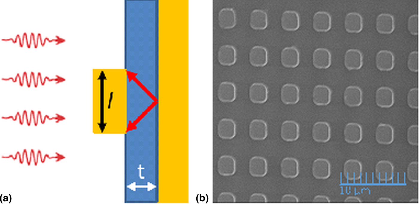
Figure 1. (a) Schematic cross-section of MIM structure. (b) SEM image of top metal.
The electromagnetic reflection from the MIM structures was simulated using Lumerical Finite-Difference Time-Domain software. The simulations shown below were 2D, meaning these were effectively infinitely long periodic strips in contrast with the fabricated squares. The light was simulated from the top-down and the polarization was in-plane with the E-field parallel to the strip width. As a test, full 3D simulations were completed on squares with widths the same size as strips. Those results showed that the wavelength position of absorption resonances is very nearly the same as the 2D case (for this polarization). With this confirmation and since the 3D simulations were computationally taxing, the 2D simulations were used to calculate resonant absorption wavelengths in comparison with the theory and fabricated samples shown here.
For device fabrication, metals, SiO2, and TiO2 films were deposited by electron beam evaporation. AlN films were deposited by reactive sputtering of aluminum in a nitrogen partial pressure. Top metals were patterned by standard contact photolithography and lift-off techniques. Figure 1(b) presents a scanning electron microscope image of aluminum squares fabricated on evaporated SiO2 and Al layers. The nominal square dimension is 2.5 µm on a 5 µm period. Although the photomask had perfect squares, the metal patterns on the finished device have rounded corners. We find that the rounding has little effect on resonance wavelengths, but there appears to be some effect on resonance strength.
IR ellipsometry (JA Woolam, IR-VASE) was used to determine the complex optical constants in the wavelength range 2–15 µm. The permittivity was modeled by fitting Gaussian oscillators to match the raw ellipsometry data using the Woolam WVASE32 software.
Reflectance spectroscopy was measured in a vacuum bench Fourier Spectrometer (Bomem DA8, Quebec, Canada) at a resolution of 4/cm. Spectrometer resources were globar source, KBr beamsplitter, and 77 K HgCdTe detector. The specular reflectance accessory (Perkin-Elmer, Waltham, Massachusetts) had an incidence angle of 8°. A gold mirror was used for reference.
Results
Figure 2 (left) presents our measured optical constants of SiO2, TiO2, and AlN, together with published silicon nitride spectra.[Reference Kischkat, Peters, Gruska, Semtsiv, Chashnikova, Klinkmüller, Fedosenko, Machulik, Aleksandrova, Monastyrskyi, Flores and Masselink8] MWIR and LWIR regions are indicated by shaded boxes. SiO2 has a strong extinction peak at 9 µm wavelength. The corresponding dispersion feature in the refractive index is nearly centered within the LWIR band. The non-monotonic variation of the index in this region allows up to three resonances by a graphical solution of Eq. (1). Thus SiO2-based LWIR MIM absorbers will exhibit poor spectral selectivity, but the multiple resonances may span the LWIR band for ordinary night vision purposes.
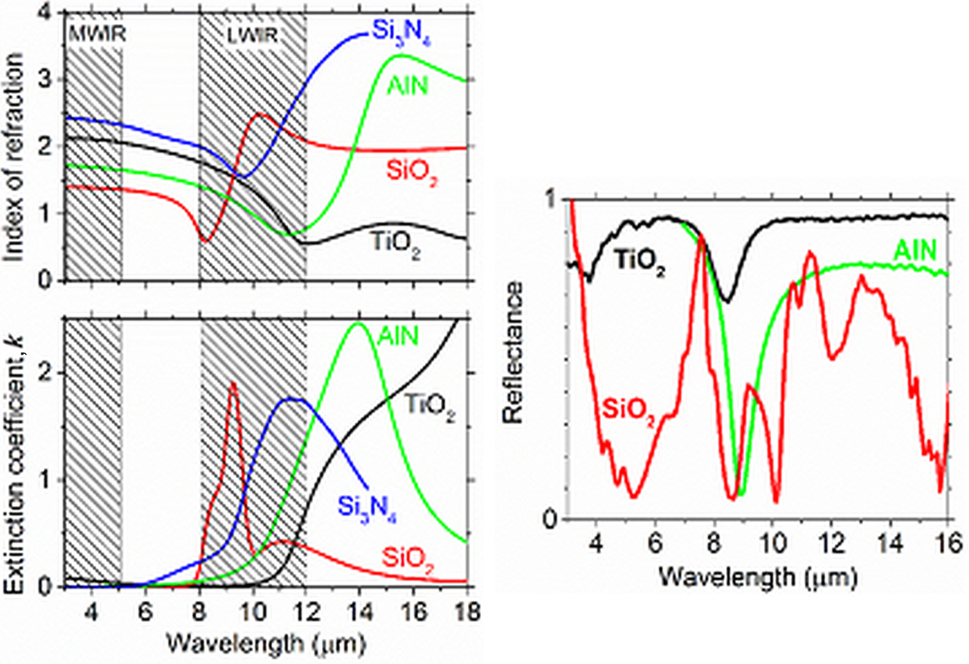
Figure 2. (a) Optical constants of AlN, TiO2, SiO2, and Si3N4. (b) Experimental reflectance spectra of AlN, TiO2, and SiO2 MIM devices.
The Si3N4 index spectrum has a broad extinction peak at 11 µm wavelength, which similarly causes a non-monotonic dependence of index on wavelength in the LWIR. Graphical solution of Eq. (1) gives up to two resonances there. Thus, Si3N4 is also a poor dielectric choice for LWIR spectral sensing, but it is also a potentially a good one for integrating the whole LWIR band, for the same reasons as SiO2.
In contrast, both TiO2 and AlN refractive indices vary monotonically in the LWIR, so that they are expected to have simple single resonances in this range. These dielectrics are therefore advantageous for wavelength-selective LWIR MIM absorbers. Broad-band LWIR losses are higher for AlN than for TiO2, which may cause broader resonances. TiO2 dispersion is the weaker of the two. Thus, TiO2 seems to be an ideal dielectric for LWIR selectivity.
At MWIR wavelengths, small values of l are required, according to Eq. (1), but sufficiently small patterns are difficult to fabricate by ordinary contact photolithograpy. Equation (1) shows that for the same dimensions, the MIM with smallest dielectric refractive index n will give the shortest resonance wavelengths. Of the four materials considered, SiO2 has the smallest MWIR index and Si3N4 the largest. AlN would be second best and might be preferred for, e.g., device-fabrication considerations.
Figure 2(b) presents representative experimental reflectance spectra of AlN, TiO2, and SiO2 based MIM devices. The (l,t) values in μm are (2.6, 0.155), (2.8, 0.095), and (4.5, 0.57), respectively. The former two have simple single LWIR resonances, while the latter has multiple resonances. These observations are consistent with the comparative discussion of dispersion effects in resonance spectra.
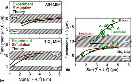
Figure 3 presents a summary of observed absorption resonances for AlN, TiO2, and SiO2 MIM devices. Resonance wavelengths are plotted as a function of the geometrical factor that appears in Eq. (1), together with predictions from that equation. Electrodynamic simulation results are also presented. The triangle symbol for the AlN simulation represents a 3D simulation result, which is nearly the same as the corresponding 2D result.
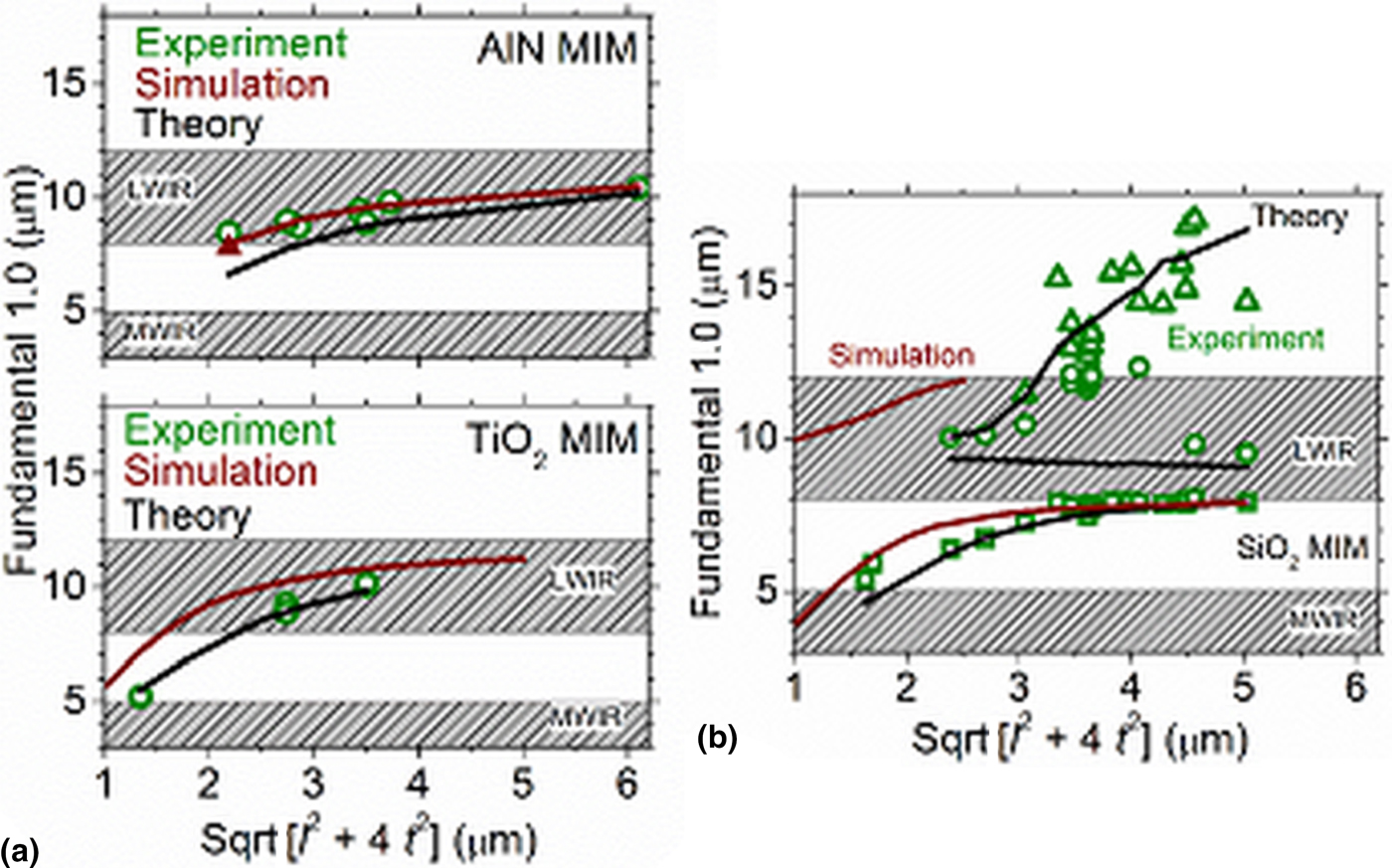
Figure 3. Comparison of experiment to theory and simulation for (a) AlN-, TiO2-, and (b) SiO2-based MIM structures.
Resonance wavelengths calculated from Eq. (1) for AlN MIMs fall below the experimental and simulated resonance positions (which agree with each other) by about 1 µm wavelength over most of the range. The disagreement is smaller for the larger geometries. In contrast, experiment and theory are in very good agreement for TiO2 MIMs, but here it is the simulation that falls below the two by 1 µm. Theory and experiment agree over much of the spectral range for the SiO2 MIMs. The prediction of multiple LWIR resonances for SiO2 MIMs is confirmed. Hence, SiO2 is problematic for the spectrally selective LWIR applications.
Figure 4(a) presents resonance wavelengths for the fundamental resonance of AlN-based MIMs as determined by electrodynamic simulations. The three different curves correspond to different values of dielectric film thickness, as indicated. The data are plotted as a function of the geometrical parameter in Eq. (1). The analytic theory predicts that if l is changed oppositely to t in such a way that the said combination of them is unchanged, we should obtain the same resonance position. In contrast, Fig. 4(a) shows a slight blue shift when t is increased holding sqrt (l 2 + 4 t 2) constant, through a range of t values typical of devices used in our experiments.
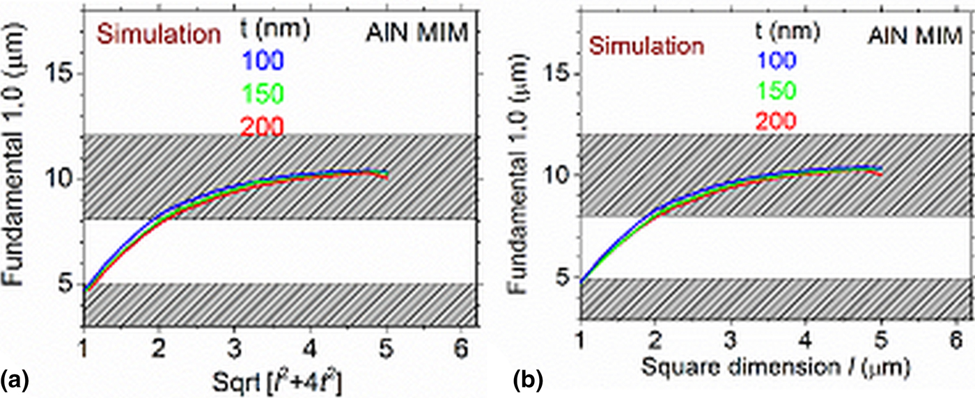
Figure 4. (a) Simulation results plotted against sqrt (l 2 + 4t 2). (b) Simulation results plotted against only the square dimension l.
Figure 4(b) plots the same simulation results but as a function of the square dimension l alone. A difference between the three curves remains, though it is slightly smaller. This result shows that the dielectric thickness does have an effect on resonance position, though the dependence is not as strong as suggested by the analytic theory Eq. (1). Whatever the true dependence on dielectric thickness happens to be, this dependence is much smaller than the scatter in our experimental data, so that it is not yet possible to experimentally constrain it. Significantly, the effect of dielectric thickness does not explain the more significant differences between theory and simulation curves observed in Fig. 3.
Discussion
ZnS has been used as the dielectric in LWIR MIM absorbers.[Reference Bouchon, Koechlin, Pardo, Haïdar and Pelouard9] This material has even lower LWIR dispersion than TiO2 and AlN, changing only by 2% over the LWIR. It has a significantly higher index, however, requiring square dimensions at the edge of what is possible with contact lithography. Furthermore, it may be an unwanted contaminant in certain deposition systems that are used for high-vacuum applications. Calculation of expected resonances positions from Eq. (1) agrees with experimentally observed values of[Reference Bouchon, Koechlin, Pardo, Haïdar and Pelouard9] within 1%.
A study[Reference Mason, Smith and Wasserman6] of LWIR resonances in MIM structures using a spin-on-glass dielectric with similar dispersion to our SiO2 showed a similarly complicated spectrum as in our Fig. 2 for this dielectric. In contrast to the work presented here, the longer wavelength absorptions were unaccounted for by simulation, and no analytic theory was presented. A sharp absorption at 7.85 µm wavelength was attributed to a very weak bump in the dielectric extinction spectrum. Oddly, however, the much stronger dielectric extinction band near 9 µm produced no significant absorption band in the MIM structure.
MIM absorbers at MWIR wavelengths have been reported using the dielectric SiN.[Reference Lefebvre, Costantini, Doyen, Lévesque, Lorent, Jacolin, Greffet, Boutami and Benisty5] The high index of this material required sub-micrometer square dimensions, as would be predicted by our Eq. (1) and Fig. 2. Our simple formula Eq. (1) with SiN index ~2.4 from Fig. 2(a) gives λ(1,0) resonance positions within ~10% of the values observed and simulated in.[Reference Lefebvre, Costantini, Doyen, Lévesque, Lorent, Jacolin, Greffet, Boutami and Benisty5]
The dielectric MgF2 was used for MWIR MIM absorbers in.[Reference Hendrickson, Vangala, Gibson, Dass, Leedy, Walker, Cleary and Guo10] The index dispersion of this material varies monotonically by 2% from 3 to 5 µm wavelength. Simulation-predicted resonances were consistently found at wavelengths longer than measured by ~5%. Calculations based on our Eq. (1) predict resonances that are consistently at a shorter wavelength than measured by ~25%. This is consistent with the general trend observed in Fig. 3 that Eq. (1) calculated resonances appear at a shorter wavelength than those from the simulation. It is also consistent, considering the THz results from,[Reference Nath, Modak, Rezadad, Panjwani, Rezaie, Cleary and Peale3] with the observation that the accuracy of Eq. (1) worsens as the wavelength is decreased from ~50 to ~3 µm. Changing the thickness of the metal squares from 77 to 100 nm caused a ~5% increase in the resonance wavelength,[Reference Hendrickson, Vangala, Gibson, Dass, Leedy, Walker, Cleary and Guo10] an effect which Eq. (1) fails to account for since permittivity and thickness of the metals are ignored.
A MWIR MIM fabricated with HfO2 and the conducting oxide indium tin oxide (ITO) showed a split resonance that was interpreted as due to the coupling of a bulk plasma resonance of the ITO and a geometric resonance of the plasmonic cavity.[Reference Park, Kang, Liu and Brongersma7] That reference's Fig. 2(h) presents the surface plasmon mode index spectrum, which shows dispersion feature like that in the SiO2 index spectrum of our Fig. 2(a). Moreover, Fig. 2(h) of[Reference Park, Kang, Liu and Brongersma7] graphically presents the resonance condition, where a triple intersection with the dispersive mode index curve indicates the expected resonances. Interestingly, their simulation and experiment reveal just two of the resonances, similarly to our simulations for the SiO2-based MIM.
Similar to,[Reference Park, Kang, Liu and Brongersma7] strong coupling between gap plasmon modes and epsilon-near-zero modes in MIM structures was demonstrated in the near-IR.[Reference Zhang, Hendrickson and Guo11] The real part of the SiO2 permittivity (ε′ = n 2−κ 2) approaches zero between 8 and 9 µm wavelength (Fig. 2), which invites a different interpretation of our LWIR results based on the coupling between gap plasmons and bulk absorption in the dielectric.
We[Reference Nath, Modak, Rezadad, Panjwani, Rezaie, Cleary and Peale3] and many others have shown that the spectral dependence on incidence angle for the subject MIM design in a regime of low dispersion is very weak up to about 60°. Strong dispersion in an isotropic dielectric would unlikely change that angle independence. However, the opposite hypothesis could be the starting point for future work.
Figure 2 showed very different absorption strength for TiO2 and AlN MIMs with similar geometric parameters. This emphasizes that these parameters have yet to be optimized. Such optimization is necessary for applications, but it is outside the focus of the present paper. However, it will be interesting to see if a systematic dependence of optimized parameters on index and dispersion will appear, and we are currently investigating this effect.
Conclusions
Four dielectrics with different degrees of refractive index dispersion in the LWIR, and with different index values in the MWIR, were investigated regarding the effect of dispersion on absorption spectrum. In the LWIR, the high dispersion insulators SiO2 and Si3N4 give rise to multiple overlapping resonances. This would suit them for absorbing broadly within LWIR band for ordinary night-vision applications. In contrast, the insulators TiO2 and AlN have low LWIR dispersion and give rise to simple single resonances that suit them for spectral-sensing applications. For the MWIR range, where all the considered insulators have low dispersion, the relatively low index of SiO2 would allow simplified MIM fabrication by contact photolithograpy.
Acknowledgments
University of Central Florida authors except Janardan Nath received partial support from AFRL contract FA8650-16-C-1738. Justin Cleary and Evan Smith acknowledge support from the Air Force Office of Scientific Research (Program Manager Dr. Gernot Pomrenke) under award number FA9550-15RYCOR162.


