


Introduction
The emergence of ultrashort pulse lasers has opened up new opportunities for high-precision processing of a wide range of materials, including dielectrics, semiconductors, and metals, enabling numerous applications in fields ranging from micromachining to photonics and life sciences. Reference Chichkov, Momma, Nolte, von Alvensleben and Tünnermann1–Reference Vorobyev and Guo3 The ability of ultrashort lasers to confine energy deposition in small regions of irradiated targets makes it possible to perform selective material modification and, at the same time, provides unique opportunities for investigation of material behavior and properties under extreme conditions of strong electronic excitation, rapid heating and cooling, and ultrafast mechanical deformation. A hierarchy of intertwined processes triggered by ultrashort laser pulses in metals, dielectrics, and semiconductors Reference Gattass and Mazur2,Reference Rethfeld, Sokolowski-Tinten, von der Linde and Anisimov4 is schematically illustrated in Figure 1 . The laser-induced processes can be roughly separated into three groups, highlighted by different colors in the figure, namely, laser excitation of optically active electronic states in the irradiated material and the initial ultrafast processes occurring in response to the electronic excitation (yellow), rapid nonequilibrium phase transformations triggered by the energy transfer from the excited electrons to atomic vibrations (green), and the subsequent cooling and solidification of the surface region of the irradiated target (turquoise).
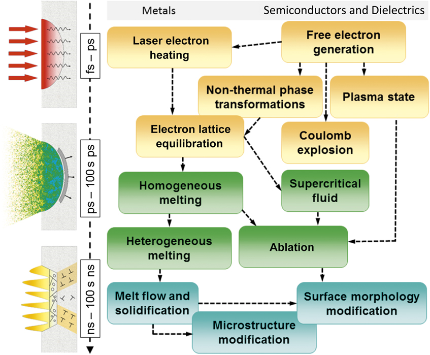
Figure 1. Typical pathways of energy dissipation and phase transformations following the excitation of a material by an ultrashort laser pulse. Note: ns, nanosecond; ps, picosecond; fs, femtosecond.
In semiconductors and dielectrics, a high concentration of free electrons promoted across the bandgap by laser excitation may lead to non-thermal phase transformations induced by transient modification of interatomic bonding. Reference Rousse, Rischel, Fourmaux, Uschmann, Sebban, Grillon, Balcou, Förster, Geindre, Audebert, Gauthier and Hulin5,Reference Hase, Fons, Mitrofanov, Kolobov and Tominaga6 Meanwhile, the excited electrons in semiconductors and dielectrics, as well as conduction-band electrons in metals, are capable of effective laser energy absorption, which may bring the material to plasma states or even produce a Coulomb explosion due to the electron emission and charging of a surface region of a dielectric target. Reference Bulgakova, Stoian, Rosenfeld, Hertel and Campbell7 The energy transfer from electrons to lattice vibrations can lead to rapid heating with rates exceeding 1014 K/s, resulting in homogeneous melting Reference Rethfeld, Sokolowski-Tinten, von der Linde and Anisimov8,Reference Ivanov and Zhigilei9 or even formation of a supercritical fluid. Reference Sokolowski-Tinten, Bialkowski, Cavalleri, von der Linde, Oparin, Meyer-ter-Vehn and Anisimov10
The extreme temperature and pressure conditions created by the rapid laser energy deposition may cause generation of unusual metastable phases, Reference Vailionis, Gamaly, Mizeikis, Yang, Rode and Juodkazis11–Reference Narayan and Bhaumik13 as well as complex surface morphology Reference Vorobyev and Guo3,Reference Vorobyev and Guo14–Reference Oboňa, Ocelík, Rao, Skolski, Römer, Huis in ‘t Veld and De Hosson16 produced in the course of photomechanical spallation Reference Paltauf and Dyer17,Reference Leveugle, Ivanov and Zhigilei18 or explosive decomposition of superheated material into a vapor–droplet mixture. Reference Martynyuk19–Reference Bulgakova and Bulgakov21 When the temperature drops below the equilibrium melting point, resolidification starts. In metals, strong laser energy localization combined with large thermal conductivity result in high cooling rates of up to 1012 K/s, Reference Lin, Spaepen and Turnbull22,Reference Wu, Christensen, Savolainen, Balling and Zhigilei23 which bring the material into a state of strong undercooling. The solidification of highly undercooled liquid may lead to the formation of unusual defect configurations, Reference Wu and Zhigilei24,Reference Sedao, Shugaev, Wu, Douillard, Esnouf, Maurice, Reynaud, Pigeon, Garrelie, Zhigilei and Colombier25 as well as nanocrystalline Reference Wu, Christensen, Savolainen, Balling and Zhigilei23 and amorphous Reference Lin, Spaepen and Turnbull22,Reference Alonso and Lopez26 structures.
In this article, we provide a brief overview of the processes previously outlined, starting from the discussion of the laser excitation and non-thermal processes occurring in the electronically excited state of the matter and following with laser-induced structural/phase transformations and laser ablation.
Laser excitation and non-thermal processes
The energy of a short laser pulse couples mainly to electrons of the irradiated material. In metals, the presence of conduction-band electrons enables the direct absorption of laser energy by electrons undergoing collisions with nuclei (i.e., by inverse bremsstrahlung). In semiconductors and dielectrics, electrons have to be excited across the bandgap before they can directly absorb photons. Reference Stuart, Feit, Herman, Rubenchik, Shore and Perry27,Reference van Driel28 The electronic excitation in materials with a bandgap may strongly modify the interatomic bonding and can lead to ultrafast phase transitions, including ultrafast melting Reference Rousse, Rischel, Fourmaux, Uschmann, Sebban, Grillon, Balcou, Förster, Geindre, Audebert, Gauthier and Hulin5 and solid–solid phase transformations. Reference Hase, Fons, Mitrofanov, Kolobov and Tominaga6 Such phase transitions are referred to as “non-thermal,” as they are directly stimulated by the laser excitation, take place in the electronically excited state on the sub-picosecond (ps) time scale, and require no electron–phonon equilibration and lattice heating.
In wide bandgap dielectrics, the main mechanisms involved in the generation of free electrons by photons having lower energy than the bandgap are multiphoton and avalanche ionizations, which are highly nonlinear processes. Reference Stuart, Feit, Herman, Rubenchik, Shore and Perry27 Multiphoton excitation (i.e., simultaneous absorption of several photons) is sensitive to the laser intensity as its probability exhibits a power law dependence on the laser intensity, which, in effect, makes the absorption process deterministic. It becomes effective for ultrashort laser pulses whose intensities are greatly increased due to the reduction of the pulse duration τp. At high laser intensities, the potential barrier for the escape of electrons from the atoms is distorted, and ionization by electron tunneling through the reduced barrier can dominate over multiphoton ionization. Reference Keldysh29 Once the electrons are excited to the conduction band, they absorb laser energy via inverse bremsstrahlung and can produce a sequence of electron–hole pairs through collisions with valence-band electrons. This process leads to avalanche multiplication of the density of conduction-band electrons.
The competition between these two mechanisms of free carrier generation is responsible for considerable improvement of machining quality with the use of ultrashort laser pulses, as illustrated in Figure 2a. Absorption of ultrashort laser pulses with durations of tens of femtoseconds (fs) and peak intensities above 1015 W/cm2 is mostly governed by the photoionization mechanisms (multiphoton or tunneling), whereas for free electrons the laser pulse is too short to trigger the avalanche process. In this case, the dependence of the lateral extension parameter q, which relates the characteristic size of a generated structure divided by the illuminated area to the incident laser fluence, is logarithmic for a Gaussian beam profile. Therefore, laser-generated cavities can be fabricated with sub-10 nm lateral and vertical precision. Reference Lenzner, Krausz, Krüger and Kautek30 For τp > 100 fs, the value of q strongly deviates from the logarithmic dependence, and the modified zone has a rugged splintered morphology, suggesting collateral damage outside the area where the laser fluence exceeds the damage threshold. This is likely to be conditioned by the “stochastic” avalanche process, which becomes efficient at longer τp. Reference Rethfeld31
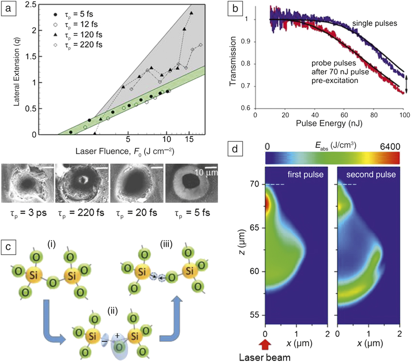
Figure 2. (a) The dependence of the lateral extension parameter q = ln(F 0/F th)/2 on laser fluence F 0 for the ablation of fused silica in air. The green region highlights values of theoretically predicted q for fluence threshold F th = 1.4 J cm–2 (τp = 5 fs) and F th = 1.9 J cm–2 (τp = 12 fs). Inserts below show scanning electron micrographs of cavities generated at different laser pulse durations. Reference Lenzner, Krausz, Krüger and Kautek30 Predominance of the multiphoton excitation mechanism for short laser pulses makes the absorption deterministic, increasing the quality of the material processing. (b) Measured transmission of a fs laser beam (800 nm, 45 fs, NA = 0.25) through a fused silica sample demonstrating the important role of self-trapped excitons (STEs) in light absorption (irregular lines). The results of a simplified modeling accounting for multiphoton and avalanche ionization and free electron trapping are shown by smooth black lines. The up-down arrow underlines the enhancement of absorption by introducing a 70-nJ prepulse in advance of the laser pulse actions. Adapted with permission from Reference Reference Grojo, Gertsvolf, Lei, Barillot, Rayner and Corkum35. © 2010 American Physical Society. (c) Schematics of the formation of defects in a-SiO2 that are responsible for accumulation effects in laser-irradiation experiments: (i) intrinsic fused silica structure; (ii) STE state (blue color shows the regions with distributed excess charges); (iii) E′-center, and non-bridged oxygen hole centers (unpaired electrons are shown by blue arrows). (d) The map of absorbed energy density predicted for laser beam propagation through fused silica in the pump-probe regime in simulations based on Maxwell’s equations. Reference Bulgakova, Zhukov, Meshcheryakov, Gemini, Brajer, Rostohar and Mocek38 Modeling reveals formation of a defect-mediated umbrella-like shield before the geometrical focus. Note: τp, pulse duration; NA, numerical aperture; a-Si, amorphous silicon; E abs, absorbed laser energy per unit volume; fs, femtosecond; ps, picosecond.
The defects that introduce intra-bandgap states also play an important role in laser excitation/absorption of wide-bandgap dielectric materials. Much work has been done on identifying the kinds of laser-generated defects in optical materials, especially in fused silica glass (bandgap of ∼9 eV), Reference Itoh and Stoneham32,Reference Pacchioni, Skuja and Griscom33 and their roles in laser-induced ionization processes. The pump-probe method, where an excitation pulse is followed by another incoming pulse with an adjustable time delay to probe the transient changes in reflection or transmission within the irradiated spot, is one of the most informative experimental techniques for such studies. Reference Martin, Guizard, Daguzan, Petite, D’Oliveira, Meynadier and Perdrix34,Reference Grojo, Gertsvolf, Lei, Barillot, Rayner and Corkum35
In particular, the characteristic lifetimes of free electrons Reference Martin, Guizard, Daguzan, Petite, D’Oliveira, Meynadier and Perdrix34 and self-trapped excitons (STEs) Reference Grojo, Gertsvolf, Lei, Barillot, Rayner and Corkum35 (∼150 fs and >30 ps, respectively) have been determined for fused silica by varying time delay between the pump and probe pulses. Figure 2b 35 demonstrates that absorption of energy from a laser beam tightly focused inside the bulk glass can be considerably enhanced by a prepulse, which couples to the sample only 3 ps in advance of the probe pulse and forms a population of STEs. The most important defects produced in fused silica by laser irradiation are schematically presented in Figure 2c. Free electrons created by the pump pulse through ionization of intrinsic glass structure are swiftly trapped into STE states. At the ps time scale, the STEs recombine with ∼0.1% of STEs evolving into permanent defects, Reference Petite, Guizard, Martin and Quéré36 E′-centers (undercoordinated silicon atom), and non-bridged oxygen hole centers (oxygen atoms bonded to one silicon atom with one unpaired electron each) with the absorption peak of 5.8 eV. Reference Pacchioni, Skuja and Griscom33 Accumulation of permanent defects is one of the key factors that affects the quality of laser processing of wide-bandgap dielectrics. Reference Mao, Quéré, Guizard, Mao, Russo, Petite and Martin37
An example of the strong effects of laser-generated defects on laser beam propagation is provided in Figure 2d, where the results of simulations based on Maxwell’s equations supplemented by hydrodynamic-type equations for free electrons oscillating in the laser field Reference Bulgakova, Zhukov, Meshcheryakov, Gemini, Brajer, Rostohar and Mocek38 are shown for pump-probe irradiation conditions with laser energy in each pulse of 0.2 μJ, τp = 150 fs, and time separation between the pulses of ∼3 ps. The simulations, which take into account the formation of STEs and their re-excitation by the probe pulse, predict the formation of a defect-mediated umbrella-like shield and explain the enhancement of light absorption in the pump-probe experiments. Reference Grojo, Gertsvolf, Lei, Barillot, Rayner and Corkum35
As demonstrated in a recent work on high-impact polystyrene Reference Naghilou, Armbruster, Kitzler and Kautek39 (see Figure 3 ), defect-mediated laser absorption can lead to the reduction of the threshold fluence for material modification with an increase in the laser beam radius, w, and the number of laser pulses applied to the same spot on the surface, N. The darkening of the modified surface in Figure 3a is due to ablation and phase separation, as illustrated by the scanning electron microscope image of the surface topography. The reduction of the threshold for large beam radii (w >> Ω–0.5, where Ω is the areal density of active low-density defects [LDDs], within the absorption volume), shown in Figure 3b, is ascribed to LDDs embedded in the matrix material and schematically illustrated in Figure 3c. Reference Naghilou, Armbruster, Kitzler and Kautek39 These defects act as donors of free electrons that can initiate an electron avalanche and, as discussed, increase laser absorption. At small beam radii (w << Ω–0.5), the laser radiation interacts mainly with the matrix material. Accumulation and incubation of LDDs upon repetitive laser irradiation significantly reduces the damage threshold (Figure 3b). This reduction is due to the generation and accumulation of optically active high-density defects (Figure 3c) with a separation distance that is smaller than the irradiation wavelength.
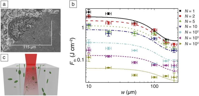
Figure 3. (a) Combination of a scanning electron micrograph (lower right) and of a reflected-light optical micrograph (upper left) of a modification site (N = 1 pulse, beam radius w = 50 ± 5 µm, fluence F 0 = 11 ± 2 J cm–2). The modified material, which appears darkened in the optical micrograph, can be correlated to the onset of morphological changes as revealed by the scanning electron micrograph. (b) The dependence of the threshold fluence F th on the laser beam radius, w, and number of pulses, N, overlain with the best fit of the extended defect model. (c) A schematic sketch of the extended defect model illustrating the presence of high-density and low-density defects. Reference Naghilou, Armbruster, Kitzler and Kautek39 Here, the red laser light is focused on the sample, and the green features represent low density defects, such as voids, cracks, and scratches. The black mesh in the absorption volume depicts high density defects.
Laser-induced structural and phase transformations
The initial non-thermal material response to the ultrafast laser excitation is quickly, within picoseconds, followed by the onset of thermal processes induced by the energy transfer from the excited electrons to atomic vibrations, commonly described as electron–phonon coupling. Rapid electron–phonon equilibration can produce ultrafast heating rates exceeding 1014 K/s, opening unique opportunities for investigating the kinetic limits of achievable superheating of solid phases. A combination of time-resolved optical, x-ray, and electron diffraction probing of short pulse laser melting Reference Lin and Elsayed-Ali40–Reference Sokolowski-Tinten, Blome, Blums, Cavalleri, Dietrich, Tarasevich, Uschmann, Förster, Kammler, Horn-von-Hoegen and von der Linde42 with theoretical analysis Reference Rethfeld, Sokolowski-Tinten, von der Linde and Anisimov8 and molecular dynamics (MD) simulations Reference Ivanov and Zhigilei9,Reference Ivanov and Zhigilei43,Reference Lin, Leveugle, Bringa and Zhigilei44 have provided important information on the time scales and mechanisms of the melting process occurring under conditions of strong superheating.
However, the short pulse laser irradiation may not only cause rapid heating and melting of localized surface or internal regions of the target, but also produce sharp temperature gradients leading to rapid quenching of the transiently melted material. In strongly absorbing materials such as metals or semiconductors, a combination of shallow depth of the laser energy deposition with high thermal conductivity of the irradiated material can lead to cooling rates approaching and even exceeding 1012 K/s. Reference Lin, Spaepen and Turnbull22,Reference Wu, Christensen, Savolainen, Balling and Zhigilei23 The cooling rates can be even higher, in excess of 1013 K/s, Reference Ivanov, Lin, Rethfeld, O’Connor, Glynn and Zhigilei45 when the laser energy deposition is confined not only within the thin surface layer of the irradiated target, but also in the lateral dimensions, creating conditions for even faster two- or three-dimensional heat transfer from the absorption region. The laterally localized laser energy deposition can be achieved by using tightly focused laser beams Reference Pronko, Dutta, Squier, Rudd, Du and Mourou46,Reference Koch, Korte, Bauer, Fallnich, Ostendorf and Chichkov47 or taking advantage of the local field enhancement in the vicinity of a tip of a scanning probe microscope. Reference Hwang, Ryu, Misra, Jeon and Grigoropoulos48,Reference Huber, Trügler, Hohenester, Prior and Kautek49
The ultrahigh rates of laser-induced cooling and the resulting resolidification, combined with the generation and relaxation of strong compressive stresses generated by the fast laser heating of the absorption region, Reference Paltauf and Dyer17,Reference Leveugle, Ivanov and Zhigilei18 create conditions for the formation of unusual metastable phases and unique material microstructures that are difficult if not impossible to produce by any other processing methods. In particular, metallic glass formation in systems not previously considered as glass formers has been demonstrated in ns- and ps-pulse laser quenching. Reference Lin, Spaepen and Turnbull22,Reference Alonso and Lopez26 Recent examples of exotic phases produced by lasers include a dense body-centered-cubic Al phase Reference Vailionis, Gamaly, Mizeikis, Yang, Rode and Juodkazis11 and new tetragonal polymorphs of silicon Reference Rapp, Haberl, Pickard, Bradby, Gamaly, Williams and Rode12 formed through ultrafast confined microexplosions generated by fs laser pulses tightly focused inside a sapphire (α-Al2O3) crystal and at the interface between a transparent amorphous silicon dioxide layer (SiO2) and an opaque crystalline Si substrate, respectively. An unusual amorphous carbon phase featuring a large fraction of sp 3-bonded carbon and a propensity for nano-/microdiamond nucleation has been generated by nanosecond laser treatment of amorphous carbon films. Reference Narayan and Bhaumik13
The laser-induced processes responsible for the generation of complex surface microstructures featuring ultrahigh densities of crystal defects are illustrated in Figure 4 , where the results of large-scale MD simulations (Figure 4a–d) and experimental transmission electron microscopy characterization of the surface modified by fs laser irradiation (Figure 4e) are shown. The snapshots presented in Figure 4a illustrate how a complex interplay of fast laser melting, rapid cooling, resolidification, and the dynamic relaxation of laser-induced stresses in the surface region of a Ag target irradiated by a 100 fs laser pulse result in the formation of a subsurface porous region covered by a nanocrystalline surface layer. Reference Wu, Christensen, Savolainen, Balling and Zhigilei23 The nanocrystalline layer with ultrafine grains (see distribution in Figure 4b) is produced by massive nucleation of crystallites triggered by a deep undercooling of the melted surface region down to ≤ 0.7T m (T m is the melting temperature) and features random crystallographic orientation of the nanograins (Figure 4b).
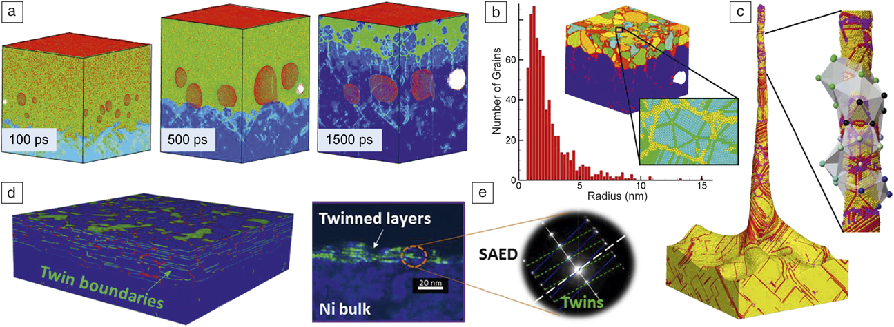
Figure 4. Short pulse laser-induced generation of complex surface microstructure (a–d) predicted in atomistic simulations and (e) observed in experiments: (a–b) Surface “swelling” and nanocrystallization of a Ag target irradiated by a 100 fs laser pulse below the spallation threshold; Reference Wu, Christensen, Savolainen, Balling and Zhigilei23 (c) formation of polyicosahedral structure of a frozen nanospike generated in the same system at higher laser fluence, in the spallation regime; Reference Wu and Zhigilei24 (d) growth twinning predicted for Ni(111) targets irradiated by 50 fs laser pulses in the simulations and (e) confirmed experimentally. Reference Sedao, Shugaev, Wu, Douillard, Esnouf, Maurice, Reynaud, Pigeon, Garrelie, Zhigilei and Colombier25 In (a), the atoms are colored by their potential energies, such that the crystalline part of the target is blue, the melted part is green, and free surfaces are red. In (b), the grain sizes are expressed in units of radii of spherical grains with equivalent volumes; (inset) the grains are colored according to their crystallographic orientation, and the atoms in the atomic view of the structure are colored such that the single and double green layers on a light blue background correspond to twin boundaries and stacking faults in the face-centered-cubic (fcc) structure. In (c), the atoms are colored such that the fcc atoms are yellow, stacking faults and twin boundaries are red, and other defects are purple. In (d), the coherent and incoherent twin boundaries generated within the top 30 nm region of the irradiated target are shown as green atomic layers and red regions within the blue fcc crystal, respectively. In (e), superimposed transmission electron microscope images highlighting the epilayers (blue) and twinned domains (green) in the laser-processed surface region of a Ni(111) target, and the results of the selected-area electron diffraction (SAED) analysis confirming the presence of twinned domains are shown. Note: fs, femtosecond; ps, picosecond.
The enlarged atomic-scale view of the surface microstructure shown for one of the nanograins in Figure 4b reveals a high density of stacking faults, twins, and nanoscale-twinned structural elements with fivefold symmetry. The formation of similar pentagonal structural elements has also been observed in frozen nanospikes generated in a MD simulation performed at a higher laser fluence, in the spallation regime discussed in the next section. Reference Wu and Zhigilei24 Structural analysis of the Ag nanospike generated in the MD simulation (Figure 4c), reveals a remarkable variability of the structural motifs coexisting in the nanospike, including a region of continuous network of pentagonal twinned structural elements arranged into a polyicosahedral structure. Reference Wu and Zhigilei24
The computational prediction of the formation of a thin nanocrystalline layer with high density of twins suggests that short pulse laser processing is a viable alternative to the severe plastic deformation Reference Valiev, Islamgaliev and Alexandrov50 or pulsed electrodeposition Reference Bufford, Wang, Liu and Lu51 techniques that are currently employed to yield maximum structural refinement and high strength of metallic materials. Moreover, the localization of the nanocrystalline structure within a thin surface layer of the target and the prominent presence of twin boundaries and pentagonal structural elements are two factors that may also increase the ductility of the laser-modified layer, Reference Fang, Li, Tao and Lu52–Reference Li, Dao, Eberl, Hodge and Gao54 a property that is generally incompatible with high strength.
Another example of unusual laser-generated defect configurations is the recent observation of nanoscale lamellar structures of interlaying twinned domains and epilayers in the surface regions of Ni(111) targets transiently melted and resolidified following exposure to fs laser pulses (Figure 4e). Reference Sedao, Shugaev, Wu, Douillard, Esnouf, Maurice, Reynaud, Pigeon, Garrelie, Zhigilei and Colombier25 The results have been explained by atomistic- and continuum-level simulations performed for the same system (Figure 4d). The simulations predict the onset of growth twinning at the resolidification front when the temperature drops below a certain critical level (0.87T m for the simulated Ni). The results of this study indicate that growth twinning can be used as a sensitive measure of the level of undercooling achieved in the transient laser-induced melting and resolidification of face-centered-cubic metal targets/grains with {111} surface orientation. In the absence of growth twinning, the structural signatures of the transient melting and resolidification (e.g., generation of a high vacancy concentration), Reference Lin, Johnson and Zhigilei55 may be too weak to be detected by ex situ experimental characterization methods. In addition, the formation of a thin layer with high density of growth twins drastically increases the strength of the surface region. Reference Zhang, Misra, Wang, Nastasi, Embury, Mitchell, Hoagland and Hirth56
Laser ablation: From photomechanical spallation to phase and Coulomb explosions
The process of laser-induced removal of material from an irradiated target, commonly called laser ablation, is at the core of many practical laser-enabled applications, including high-precision cutting and drilling, surface nanostructuring, pulsed laser deposition of films and coatings, and generation of nanoparticles with narrow size distributions and well-controlled compositions. Several mechanisms driving the collective ejection of material from the irradiated target are briefly outlined in the next section.
As mentioned, the fast rate of energy deposition by short laser pulses may lead to the generation of compressive stresses. The laser-generated stresses are particularly high in the regime of stress confinement, Reference Paltauf and Dyer17,Reference Leveugle, Ivanov and Zhigilei18 when the time of the laser heating (defined by the laser pulse duration, τp, or the time of the electron–phonon equilibration, τe–ph, whichever is longer) is shorter than the time required for the mechanical relaxation (expansion) of the heated volume, in other words, max{τp , τe–ph} ≤ L p /C s, where C s is the speed of sound in the target material and L p is the effective depth of the laser energy deposition (optical penetration depth or, in the case of metals, the depth of diffusive/ballistic energy transport during the time of the electron–phonon equilibration). Reference Leveugle, Ivanov and Zhigilei18
The interaction of the laser-induced compressive stresses with the free surface of the irradiated sample can result in the generation of a tensile wave sufficiently intense to cause the formation subsurface voids (Figure 4a). The growth and percolation of the voids may lead to the separation and ejection of a top layer from the target. Analogous to the term “spallation,” commonly used to describe the dynamic fracture that results from the reflection of a shock wave from the back surface of a sample, material ejection driven by the relaxation of laser-induced stresses is commonly referred to as photomechanical spallation (admittedly, “cavitation” would be a more appropriate term when the photomechanical processes take place in the melted part of the target).
Further increase in the laser fluence above the spallation threshold results in the separation and ejection of thinner layers and/or multiple droplets from the target, and, at a sufficiently high laser fluence, induces a transition to a different ablation regime commonly referred to as “phase explosion” or “explosive boiling.” In this regime, the melted surface region of the irradiated target is overheated above the limit of thermodynamic stability of the liquid phase, Reference Martynyuk19–Reference Bulgakova and Bulgakov21 leading to a rapid decomposition of the overheated melted material into a mixture of vapor and liquid droplets. The transition from photomechanical spallation to phase explosion is signified by a sharp (threshold-like) increase in the amount of the vapor-phase atoms in the ejected plume, Reference Wu and Zhigilei57,Reference Zhigilei and Garrison58 which reflects the difference in the physical mechanisms responsible for the material ejection in these two regimes. An explosive release of vapor, rather than the relaxation of photomechanical stresses, provides the main driving force for the collective ejection of the overheated surface region of the target in the regime of phase explosion. In the case of ablation by longer laser pulses, in the absence of stress confinement, spallation is not activated and explosive boiling is the mechanism responsible for the direct transition from the regime of surface melting and evaporation to the phase explosion. Reference Bulgakova and Bulgakov21,Reference Zhigilei and Garrison58
Due to the spatial variation of laser intensity within laser beams that often have Gaussian profiles, photomechanical spallation and phase explosion may coexist and jointly contribute to the material ejection induced by the same laser pulse. This is illustrated by Figure 5a, where a “mosaic approach” combining the results of simulations performed at different local laser fluences is used for representation of the laser-induced processes at the scale of the whole laser spot. Reference Wu and Zhigilei57 Two distinct sections can be easily identified within the laser spot: the central area, where the overheated top part of the surface region undergoes an explosive decomposition into vapor and liquid droplets, and the periphery of the spot, where spallation of well-defined liquid layers connected to the bulk of the target by transient foamy structures of interconnected liquid regions is observed. Although the liquid layers observed in individual simulations are flattened by the application of periodic boundary conditions, the integral picture of ablation by the Gaussian laser beam is likely to involve the peel off of a continuous liquid layer with its thickness decreasing toward the center of the laser spot, as shown schematically in Figure 5a by gray stripes and directly observed in Figure 5d, where a snapshot from a simulation of Au surface nanostructuring by periodically modulated energy deposition realized in two-beam interference experiments is shown. Reference Ivanov, Lipp, Blumenstein, Kleinwort, Veiko, Yakovlev, Roddatis, Garcia, Rethfeld, Ihlemann and Simon59
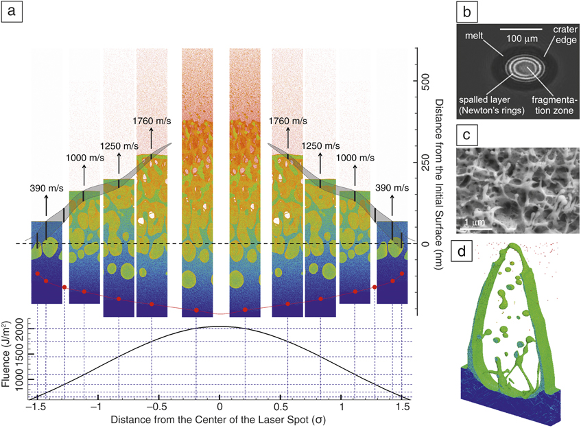
Figure 5. (a) Visualization of laser ablation obtained in a series of molecular dynamics (MD) simulations of an Al target irradiated by a 100 fs laser pulse. Reference Wu and Zhigilei57 The laser beam has a Gaussian spatial profile with the standard deviation σ and a peak absorbed laser fluence of 2050 J/m2. The snapshots are taken at the same time of 150 ps after the laser pulse and are aligned with locations within the laser spot that correspond to the values of local fluence used in the simulations, as shown in the lower part of the panel. The atoms in the snapshots are colored by their potential energy, from blue for low energy atoms in the bulk of the target to red for the vapor-phase atoms. The red dots connected by the red line mark the location of the liquid–crystal interface. (b) Optical micrograph taken at 800 ps after irradiation of a GaAs target by a 110 fs laser pulse. Reference Ionin, Kudryashov, Seleznev and Sinitsyn60 (c) Scanning electron microscope image of surface morphology generated on a Au target irradiated by two 60 fs laser pulses. Reference Vorobyev and Guo14 (d) Result of MD simulation of surface nanostructuring by the two-beam interference technique. Reference Ivanov, Lipp, Blumenstein, Kleinwort, Veiko, Yakovlev, Roddatis, Garcia, Rethfeld, Ihlemann and Simon59 The snapshot is taken at 800 ps after the laser pulse and colored such that the crystalline and melted parts of the target are blue and green, respectively. Note: fs, femtoseconds; ps, picoseconds.
Both spallation and phase explosion provide channels for effective transformation of the energy deposited by the laser irradiation into material disintegration and vaporization, thus creating conditions for rapid cooling and freezing of the transient liquid structures generated in laser spallation or ablation. Reference Wu and Zhigilei24,Reference Wu and Zhigilei57 Indeed, the temperature of the liquid–crystal interface, shown in Figure 5a by the red line connecting red dots, drops down to the melting temperature of Al by ∼600 ps, and the interface starts to move up, toward the surface. One can expect that the solidification process will freeze (either by epitaxial regrowth of the substrate or by rapid homogeneous nucleation of the solid phase under strong undercooling conditions) some of the evolving liquid structures, leading to the formation of a complex surface nanostructure, Reference Vorobyev and Guo14–Reference Oboňa, Ocelík, Rao, Skolski, Römer, Huis in ‘t Veld and De Hosson16 such as the one shown in Figure 5c.
The occurrence of both spallation and phase explosion processes within the same laser spot can also be related to the results of pump-probe experiments, Reference Sokolowski-Tinten, Bialkowski, Cavalleri, von der Linde, Oparin, Meyer-ter-Vehn and Anisimov10,Reference Ionin, Kudryashov, Seleznev and Sinitsyn60,Reference Agranat, Anisimov, Ashitkov, Zhakhovskii, Inogamov, Nishihara, Petrov, Fortov and Khokhlov61 where the observation of optical interference patterns (Newton’s rings) can be explained by the spallation of a thin liquid layer from the irradiated target and the absence of interference fringes in the central part of the laser spot (Figure 5b) can be attributed to the transition to the phase explosion regime.
Another possible ablation mechanism intimately connected to the conditions of electronic nonequilibrium, discussed at the beginning of this article, is the electrostatic disintegration of a superficial layer of irradiated material caused by effective photo- and thermionic emission of electrons and associated positive charging of the material surface, the so-called Coulomb explosion (CE). Reference Bulgakova, Stoian, Rosenfeld, Hertel and Campbell7 This mechanism of ablation, which manifests itself as highly energetic ion emission, has been widely debated for different materials. Reference Stoian, Ashkenasi, Rosenfeld and Campbell62–Reference Kaplan, Lenner and Palmer65 The main feature of CE is the momentum scaling of differently charged ions and ions of different species in time-of-flight signals Reference Stoian, Ashkenasi, Rosenfeld and Campbell62 that suggests their emission and acceleration by the electric field.
The occurrence of CE is defined by the competition between the laser-induced electron photoemission leaving behind a positively charged surface layer of the material and the neutralization of the positive charge by the free electron current from the material bulk. It was proven theoretically that at fluences slightly above the ablation threshold, CE can be realized in wide-bandgap dielectrics while, in semiconductors and metals, high mobilities of charge carriers prevent accumulation of the positive charge up to the level sufficient for disintegration of a surface layer by electrostatic repulsive forces. Reference Bulgakova, Stoian, Rosenfeld, Hertel and Campbell7 When CE does occur, the exploded material leaves behind a smooth undamaged surface Reference Stoian, Ashkenasi, Rosenfeld and Campbell62 that makes this ablation mode highly attractive for nanoscale applications (e.g., ultrafine material polishing). There are indications of the possibility of CE in semiconductors at laser fluences above the plasma formation level. Reference Roeterdink, Juurlink, Vaughan, Dura Diez, Bonn and Kleyn63 However, at such conditions, the ions originating from the CE constitute a small fraction of the ablation products and are masked by the thermal ablation ions, including those accelerated by the plume double layer (two oppositely charged parallel layers created in the front of expanding plasmas due to faster electrons running ahead of slower ions). Reference Roeterdink, Juurlink, Vaughan, Dura Diez, Bonn and Kleyn63,Reference Bulgakova, Bulgakov, Zhukov, Marine, Vorobyev and Guo66 In thin metal wires exposed to ultraintense laser pulses, a substantial fraction of electrons is carried away from the wire by the laser field, resulting in electrostatic disintegration of the ionic lattice left behind. Reference Borghesi, Romagnani, Schiavi, Campbell, Haines, Willi, Mackinnon, Galimberti, Gizzi, Clarke and Hawkes67
Concluding remarks
Rapid expansion of practical applications of ultrashort pulse lasers into new areas where precise nanoscale control of material modification is required can only be sustained with an improved fundamental understanding of laser–materials interactions. The ability to achieve high spatial resolution in material modification and microstructure engineering usually relies on fast and highly localized energy deposition that, unavoidably, creates conditions of strong electronic, thermodynamic, and mechanical nonequilibrium.
Theoretical and computational description of the materials behavior far from equilibrium is challenging and requires the revision of existing (or the development of new) theoretical models and computational approaches. In particular, the intricate connections between the ultrafast material response to laser excitation, generation of crystal defects, phase transformations, and mass transfer occurring under highly nonequilibrium conditions can only be accounted for by combining the research expertise and theoretical approaches from different disciplines. Close interdisciplinary collaborations and innovative design of new multiscale approaches incorporating dissimilar physical concepts and operating at different time and length scales are needed for disruptive progress in the theoretical and computational description of laser–materials interactions.
On the experimental side, the development of advanced imaging techniques capable of providing time-resolved information on the ultrafast structural and phase transformations is crucial for gaining fundamental understanding of laser-induced processes. Not unlike the theoretical efforts, the imaging/probing of different laser-induced processes requires a combination of optical pump-probe techniques with variable delay and temporal pulse-shaping, advanced diffractive imaging of transient atomic dynamics and ultrafast structural transformations, as well as the imaging/probing of ablation plume dynamics capable of tracking the spatial distribution and physical characteristics of different plume components.
Overall, investigations of ultrafast laser–materials interactions are expanding the limits of the fundamental understanding of material behavior under extreme conditions and providing opportunities for the generation of new material phases and microstructures.
Acknowledgments
M.V.S., C.W., and L.V.Z. acknowledge financial support from the National Science Foundation (NSF) through Grants CMMI-1301298 and CMMI-1436775 and computational support provided by the Oak Ridge Leadership Computing Facility (INCITE Project MAT130) and NSF through the Extreme Science and Engineering Discovery Environment (Project TGDMR110090). L.V.Z. and W.K. also acknowledge support from the Austrian Science Fund (FWF) through the Lise Meitner Programme (Project M 1984). N.B., D.S.I., and B.R. acknowledge support by the Deutsche Forschungsgemeinschaft (Projects RE 1141/14 and RE 1141/15). N.M.B. and T.J.-Y.D. acknowledge support of the state budget of the Czech Republic (Project L01602). T.J.-Y.D. also acknowledges funding from the European Commission for the Marie Skłodowska-Curie Individual Fellowship (Project 657424).
Maxim V. Shugaev is a doctoral candidate at the University of Virginia. He received his MS degree in physics in 2012 from Novosibirsk State University, Russia. His research interests include the generation of crystal defects in short pulse laser processing, molecular dynamics and continuum-level modeling, laser interaction with matter, nonlinear acoustics, and high-performance computing. Shugaev can be reached by email at mvs9t@virginia.edu.

Chengping Wu is a research scientist in the Department of Materials Science and Engineering at the University of Virginia, where he develops and implements computational models to perform petascale simulations to investigate the fundamental processes of laser–materials interactions. He received his BS degree in applied physics in 2007 from the University of Science and Technology of China, and PhD degree in physics in 2013 from the University of Virginia. His interests include laser–materials interactions, surface processes, nanomaterials, and high-performance computing. Wu can be reached by email at cw5xj@virginia.edu.

Oskar Armbruster is a postdoctoral researcher at the Institute of Applied Physics at Johannes Kepler University, Linz, Austria. He studied engineering physics at Johannes Kepler University from 2005–2010, and received his PhD degree from the University of Vienna, Austria, in 2016. His research interests focus mainly on experimental femtosecond (fs) laser–matter interaction and fs laser technology, as well as plasmonics and light manipulation. Armbruster can be reached by email at oskar.armbruster@univie.ac.at.

Aida Naghilou is a doctoral candidate in the Department of Physical Chemistry at the University of Vienna, Austria. She received her master’s degree at the University of Vienna in 2014. Her research interests include ultrafast lasers, laser–material interactions, pulse shaping, nanoparticle generation in liquid, and pump-probe spectroscopy. Naghilou can be reached by phone at +431 427752447 or by email at aida.naghilou@univie.ac.at.

Nils Brouwer is a doctoral candidate at the University of Kaiserslautern, Germany. His studies focus on the field of ultrafast dynamics of laser-excited solids, especially dielectrics, and their description using Boltzmann collision integrals. He received his degree in physics from the University of Kaiserslautern in 2012. Brouwer can be reached by phone at +49-631-205-4717 or by email at brouwer@physik.uni-kl.de.
Dmitry S. Ivanov is a senior research scientist at the University of Kassel and the University of Kaiserslautern, Germany. He earned his PhD degree at the University of Virginia. He was one of the first developers of the atomistic-continuum approach in molecular dynamics-based simulations of short laser pulse interaction with metals. Due to the growing popularity of this model, it was later extended to large-scale simulation of short laser pulse nanostructuring of metal targets and semiconductors. He is a co-author of 35 research papers and monographs. Ivanov can be reached by phone at +491637558755 or by email at ivanov@uni-kassel.de.
Thibault J.-Y. Derrien obtained his PhD degree in 2012 at the Aix-Marseille University, France, in continuum modeling of laser–matter interaction. After completing postoctoral work on the theory of laser-induced periodic surface structure formation at Bundesanstalt für Materialforschung und -prüfung, Berlin, Germany, he received an individual Marie Skłodowska-Curie Fellowship of the EU Horizon 2020 Programme to theoretically investigate processes in semiconductors irradiated by ultrashort laser pulses at the HiLASE Centre. Derrien can be reached by phone at +420 314 007 709 and by email at derrien@fzu.cz.

Nadezhda M. Bulgakova is Research Program Leader (RP4) of the HiLASE Centre, Czech Republic, and Chief Researcher at the Institute of Thermophysics SB RAS, Russian Federation. She received her PhD and Dr. Sci. degrees from the Russian Academy of Sciences. Her research interests include processes in solid targets absorbing laser radiation, dynamics of plasma plumes during pulsed laser ablation of solids, and cluster formation in free gaseous jets and laser-ablation plumes. She has published more than 160 articles and book chapters in English and Russian. Bulgakova can be reached by phone at +420 314007709 or by email at bulgakova@fzu.cz.
Wolfgang Kautek has been a full professor and Head of the Department of Physical Chemistry at the University of Vienna, Austria, since 2004. He holds a diploma in chemical engineering from the Vienna University of Technology, Austria, and a doctoral degree from the University of Technology Berlin, Germany. Previously, he served as a research scientist at the University of Kentucky, the Fritz Haber Institute of the Max Planck Society, the IBM San Jose Research Laboratory, and the Siemens Research Center. He was head of the Laboratory for Thin Film Technology of the Federal Institute for Materials Research and Testing, Germany and adjunct professor at the Free University Berlin, Germany. Kautek can be reached by phone at +43 664 6027752470 or by email at wolfgang.kautek@univie.ac.at.

Baerbel Rethfeld has been a Heisenberg Professor of Applied Theoretical Physics at the University of Kaiserslautern, Germany, since 2013. She received her PhD degree from the University of Braunschweig in 1999. She was previously employed at the University of Essen, Germany; L.D. Landau Institute for Theoretical Physics, Russia; and GSI Helmholtz Institute, Germany. In 2007, she established her own research group at the University of Kaiserslautern after she was awarded an Emmy Noether Grant from the German Research Foundation. Her research interests include the theoretical description of ultrafast dynamics of laser-excited solids with an emphasis on nonequilibrium processes. Rethfeld can be reached by phone at +49-631-205-2385 or by email at rethfeld@physik.uni-kl.de.
Leonid V. Zhigilei is a professor of materials science and engineering at the University of Virginia. He studied materials science at Leningrad Polytechnic Institute and completed his PhD dissertation work at Tomsk State University and St. Petersburg State University, Russia. Prior to joining the faculty of the University of Virginia, he was a postdoctoral researcher in the Department of Chemistry at The Pennsylvania State University. His research interests include multiscale modeling of materials behavior far from equilibrium, mechanisms of phase transformations, nanomaterials, and surface processes. Zhigilei can be reached by phone at 434-243-3582 or by email at lz2n@virginia.edu.


