


Introduction
Electronic devices providing extensive functionality and tremendous convenience have become essential in society today. The demand for stable, long-operating electronic devices has long motivated studying their reliability. In 2012, a new type of electronics with a goal antithetical to conventional reliability emerged under the name “transient electronics”—electronic devices that disappear within a specified time frame.Reference Hwang, Tao, Kim, Cheng, Song, Rill, Brenckle, Panilaitis, Won, Kim, Yu, Ameen, Li, Su, Yang, Kaplan, Zakin, Slepian, Huang, Omenetto and Rogers1
Transient electronics offer new opportunities in applications in alternative and emerging fields that previous permanent electronics cannot achieve. For example, a biodegradable electronics device can be implanted inside the body to diagnose and treat patients without needing surgical removal after its function ends, thus reducing the risk of surgical accidents and infection.Reference Kang, Murphy, Hwang, Lee, Harburg, Krueger, Shin, Gamble, Cheng, Yu, Liu, McCall, Stephen, Ying, Kim, Park, Webb, Lee, Chung, Wie, Gujar, Vemulapalli, Kim, Lee, Cheng, Huang, Lee, Braun, Ray and Rogers2–Reference Lee, Kim, Harburg, Park, Ma, Pan, Kim, Lee, Kim, Jang, Kang, Huang, Kim, Lee, Leal and Rogers5 It also provides waste-free technology—the device self-degrades into eco-compatible, easily disposable byproducts, and is thus attractive for wearable and patch-type electronic devices.Reference Hwang, Tao, Kim, Cheng, Song, Rill, Brenckle, Panilaitis, Won, Kim, Yu, Ameen, Li, Su, Yang, Kaplan, Zakin, Slepian, Huang, Omenetto and Rogers1,Reference Hwang, Huang, Seo, Song, Kim, Hage-Ali, Chung, Tao, Omenetto, Ma and Rogers6 This type of electronics offers hardware-level security by self-destruction on demand of specified areas such as memory so as not to expose unwanted information and device features.Reference Hernandez, Kang, Lee, Hwang, Kaitz, Inci, Park, Chung, Sottos, Moore, Rogers and White7–Reference Lee, Jeong, Liu, Zhang, Shi, Kang, Kim, Kim, Lee, Kim, Jang, Yin, Kim, Banks, Paik, Huang and Rogers10
The history of general transient materials has its roots in biodegradable materials. Biodegradable materials have been widely used, including medical sutures, polymer scaffolds for tissue regeneration, metals and alloys for temporary bone joints or stents to minimize restenosis, active glass to promote bone regeneration, and as vehicles for drug delivery.Reference Prakasam, Locs, Salma-Ancane, Loca, Largeteau and Berzina-Cimdina11,Reference Gunatillake and Adhikari12 Most applications, however, have been limited to using structures or biochemically reactive species; advanced functions such as comprehensive sensing and delicate treatment were not yet possible. The first study exploring biodegradable electronics entailed constructing an organic thin-film transistor using biodegradable semiconducting and dielectric materials.Reference Bettinger and Bao13 A subsequent study expanded the biodegradable electronic materials possible by adopting natural chemicals such as indigo, yellow G, and indanthrene, and synthesizing artificial polymers such as poly(diketopyrrolopyrrole-p-phenylenediamine) (PDPP-PD).Reference Irimia-Vladu, Troshin, Reisinger, Shmygleva, Kanbur, Schwabegger, Bodea, Schwödiauer, Mumyatov, Fergus, Razumov, Sitter, Sariciftci and Bauer14,Reference Lei, Guan, Liu, Lin, Pfattner, Shaw, McGuire, Huang, Shao, Cheng, Tok and Bao15
Hwang et al. reported outstanding results in transient electronics in 2012 that suggested that electronics-grade single-crystal Si in nanometer-scale membrane form dissolves within a reasonable time frame (on the order of a few to 10 nm per day) in a phosphate buffer solution (PBS).Reference Hwang, Tao, Kim, Cheng, Song, Rill, Brenckle, Panilaitis, Won, Kim, Yu, Ameen, Li, Su, Yang, Kaplan, Zakin, Slepian, Huang, Omenetto and Rogers1 They created fully functional electrical components, ranging from active transistors and diodes to passive inductors and capacitors, using single-crystal Si nanomembrane semiconductors, SiO2 and MgO dielectrics, and Mg electrodes on biodegradable silk substrates. In addition, they showed that all of these electronics are dissoluble. This study laid out the concept of transient electronics and also pointed to the possible translation of conventional Si-based electronics to water-soluble transient electronics such as semiconductors, piezoresistivity sensors, photovoltaic energy harvesters, and photoconductive sensors.Reference Hwang, Tao, Kim, Cheng, Song, Rill, Brenckle, Panilaitis, Won, Kim, Yu, Ameen, Li, Su, Yang, Kaplan, Zakin, Slepian, Huang, Omenetto and Rogers1 The transient electronic devices now available range from metal oxide semiconductor field-effect transistors (MOSFETs), complementary metal oxide semiconductors (CMOSs), and logic circuits to sensors for temperature, strain, pressure, thermodiffusion, and flow rates.Reference Hwang, Tao, Kim, Cheng, Song, Rill, Brenckle, Panilaitis, Won, Kim, Yu, Ameen, Li, Su, Yang, Kaplan, Zakin, Slepian, Huang, Omenetto and Rogers1,Reference Kang, Murphy, Hwang, Lee, Harburg, Krueger, Shin, Gamble, Cheng, Yu, Liu, McCall, Stephen, Ying, Kim, Park, Webb, Lee, Chung, Wie, Gujar, Vemulapalli, Kim, Lee, Cheng, Huang, Lee, Braun, Ray and Rogers2,Reference Hwang, Huang, Seo, Song, Kim, Hage-Ali, Chung, Tao, Omenetto, Ma and Rogers6,Reference Hwang, Kim, Tao, Kim, Kim, Yu, Panilaitis, Jeong, Song, Omenetto and Rogers16
The potential uses of transient electronics have already been demonstrated in biodegradable devices with clinically relevant medical applications. A medical device has been proposed to diagnose traumatic brain injury, which has an incubation period and thus requires temporary monitoring of intracranial pressure.Reference Kang, Murphy, Hwang, Lee, Harburg, Krueger, Shin, Gamble, Cheng, Yu, Liu, McCall, Stephen, Ying, Kim, Park, Webb, Lee, Chung, Wie, Gujar, Vemulapalli, Kim, Lee, Cheng, Huang, Lee, Braun, Ray and Rogers2 Fully biodegradable, miniaturized pressure sensors have been made of nanoporous Si for rigid volumetric structure, biodegradable poly(lactic-co-glycolic acid) (PLGA) for flexible membranes responsive to external pressure, Si nanomembranes for strain sensing, and SiO2 for the encapsulation layer. The pressure sensor delivered continuous monitoring of intracranial pressure in a rat model with a wireless interface. These results validate biodegradable electronics in animals at clinically acceptable performances. Subsequent research on measuring electroencephalography (EEG) and electrocorticography (ECoG) also supports the effectiveness of transient electronics.Reference Yu, Kuzum, Hwang, Kim, Juul, Kim, Won, Chiang, Trumpis, Richardson, Cheng, Fang, Thomson, Bink, Talos, Seo, Lee, Kang, Kim, Lee, Huang, Jensen, Dichter, Lucas, Viventi, Litt and Rogers3 A biodegradable wireless stimulator has recently been used therapeutically to accelerate the regeneration of function of injured peripheral nerves, thus extending the use of transient electronics from sensing to therapy.Reference Koo, MacEwan, Kang, Won, Stephen, Gamble, Xie, Yan, Chen, Shin, Birenbaum, Chung, Kim, Khalifeh, Harburg, Bean, Paskett, Kim, Zohny, Lee, Zhang, Luo, Ji, Banks, Lee, Huang, Ray and Rogers4
The development of transient electronic devices requires research in all areas of materials science and engineering, including analysis of material behaviors, development of process and fabrication technologies, and verification and application in devices, and on a system level (Figure 1). A database of transient organic and inorganic materials (Figure 1a) has been established from dissolution mechanism studies of potential materials, including dissolution chemistry and kinetics under various environmental conditions (temperature, pH, and other ion species in fluids).Reference Hwang, Tao, Kim, Cheng, Song, Rill, Brenckle, Panilaitis, Won, Kim, Yu, Ameen, Li, Su, Yang, Kaplan, Zakin, Slepian, Huang, Omenetto and Rogers1,Reference Kang, Hwang, Cheng, Yu, Kim, Kim, Huang and Rogers17–Reference Kang, Park, Kim, Hwang, Cheng, Shin, Chung, Kim, Yin, Lee, Lee and Rogers20 Accurate control of lifetime is available by passively protecting the device with biodegradable encapsulation or actively initiating the degradation reaction by triggering (Figure 1b). Fabrication strategies such as transfer-printing and solution-printing processes (Figure 1c) are also being widely developed for integrated transient electronic materials, from the component level to circuit and system levels (Figure 1d).Reference Hwang, Kim, Tao, Kim, Kim, Yu, Panilaitis, Jeong, Song, Omenetto and Rogers16,Reference Hwang, Song, Huang, Cheng, Kang, Kim, Kim, Yu, Huang and Rogers21,Reference Chang, Fang, Bower, Song, Yu and Rogers22 Results have yielded various devices for measurement, logic processing, and activation of biomedical and eco-friendly sensors and actuators such as intracranial pressure monitor, environmentally friendly stimulator, and a wireless self-destructive heater (Figure 1e). Applications continue to expand.Reference Hwang, Tao, Kim, Cheng, Song, Rill, Brenckle, Panilaitis, Won, Kim, Yu, Ameen, Li, Su, Yang, Kaplan, Zakin, Slepian, Huang, Omenetto and Rogers1–Reference Hwang, Huang, Seo, Song, Kim, Hage-Ali, Chung, Tao, Omenetto, Ma and Rogers6

Figure 1. Representative research areas of transient electronics in materials science and engineering. (a) Dissolution chemistry studies in inorganic and organic electronic materials. Adapted with permission from References 1 and 15. © 2012 AAAS and 2017 Proceedings of the National Academy of Science, respectively. (b) Lifetime controlling method using passive encapsulation and active triggering. Adapted with permission from References 7 and 17. © 2014 Wiley. (c) Fabrication strategy of transient electronics using solution processing for a wafer-scale approach. Adapted with permission from References 21, 25, and 22. © 2014 Wiley and 2017 Proceedings of the National Academy of Science, respectively. (d) Example of transient device formed from electric components (array of metal oxide semiconductor field-effect transistors, top) for integrated circuits (ring oscillator, mid) and system-level medical device (electrical nerve stimulator, bottom). Adapted with permission from References 1, 4, and 6. © 2012 AAAS, 2018 Springer Nature, and 2013 Wiley, respectively. (e) Representative application fields of transient electronics. Adapted with permission from References 2 and 9. © 2016 Springer Nature, 2018 Springer Nature, and 2015 Wiley, respectively. Note: PE-CVD, plasma-enhanced chemical vapor deposition; ALD, atomic layer deposition; PDPP-PD, poly(diketopyrrolopyrrole-p-phenylenediamine); TMSO, trimethylsilyl-o; TMSC, trimethylsilyl-cellulose; PLGA, poly(lactic-co-glycolic acid).
This issue of MRS Bulletin introduces recent developments and advances in transient electronics devices and is organized into five topics. The article by Choi et al. is the overall development of transient electronics using inorganic materials.Reference Choi, Koo and Rogers23 The transient behavior and biocompatibility of key elements are discussed in comprehensive electrochemical terms, and a biomedical system is introduced as a representative example. The article by Liu et al. is the development of biodegradable organic materials for transient electronics.Reference Liu, Tran, Feig and Bao24 Soft and bio-friendly devices are available that use organic materials for flexible, stretchable applications. Biodegradable polymers are also widely highlighted as substrates and encapsulation layers that are essential for protection electronics. In their article in this issue, Han et al. discuss a fabrication technology that integrates reactive transient materials into devices.Reference Han, Ko, Shin and Hwang25 This method focuses on the integration of inorganic and organic transient materials to exploit their complementary electrical and mechanical properties. The article by Jia et al. introduces a transient energy source as a representative example of a fully formed device.Reference Jia, Wang, Lee, Yu and Wallace26 The materials, structure, and electronic device design for energy-storage technology are reviewed, including energy-storage devices such as batteries and capacitors, and energy-harvesting technologies such as piezoelectricity, tribogenerators, photovoltaics, and wireless power-transmission technologies. The final article by You et al.Reference You, Zhao, Guo and Mei27 discusses on-demand control of transient device lifetimes, so-called trigger-transient electronics. Strategies to remove materials via various stimuli such as light and heat as well as solution reactions are reviewed. In the sections that follow, we provide a brief overview of each of these topics as presented in the articles in this issue.
Biodegradable inorganic materials for transient electronics
Inorganic transient electronics that exploit the excellent electrical properties and stability of inorganic materials have expanded rapidly after the initial demonstration of the dissolution of electrical-grade single-crystal Si nanomembranes. Hwang et al. showed that ∼100-nm-thick single-crystal Si dissolved in a phosphate buffer solution at 37°C at a rate of ∼3 nm/day, suggesting the potential use of Si as transient or biodegradable electrical functional materials.Reference Hwang, Tao, Kim, Cheng, Song, Rill, Brenckle, Panilaitis, Won, Kim, Yu, Ameen, Li, Su, Yang, Kaplan, Zakin, Slepian, Huang, Omenetto and Rogers1 The versatile electrical properties of Si provide various types of transient electronics, including electronic components such as transistors, diodes, and inductors, logic circuits, and optical, temperature, and strain sensors.Reference Hwang, Tao, Kim, Cheng, Song, Rill, Brenckle, Panilaitis, Won, Kim, Yu, Ameen, Li, Su, Yang, Kaplan, Zakin, Slepian, Huang, Omenetto and Rogers1 The study of dissolution chemistry and kinetics of potential transient electronic materials has naturally become important. Follow-up studies demonstrate that Ge, SiGe, and amorphous indium gallium zinc oxide (a-IGZO) are also dissoluble in a phosphate buffer solution and can be alternative semiconductor layers.Reference Kang, Park, Kim, Hwang, Cheng, Shin, Chung, Kim, Yin, Lee, Lee and Rogers20,Reference Jin, Kang, Cho, Han, Chung, Lee, Shin, Baek, Kim, Lee and Rogers28 Dissolution kinetics strongly depend on materials microstructure such as density of films and crystallinity, and on environmental conditions such as temperature, pH, and ion species.Reference Hwang, Tao, Kim, Cheng, Song, Rill, Brenckle, Panilaitis, Won, Kim, Yu, Ameen, Li, Su, Yang, Kaplan, Zakin, Slepian, Huang, Omenetto and Rogers1,Reference Kang, Hwang, Cheng, Yu, Kim, Kim, Huang and Rogers17–Reference Lee, Yu, Song, Farimani, Vitale, Xie, Yoon, Kim, Richardson, Luan, Wu, Xie, Lucas, Crawford, Mei, Feng, Huang, Litt, Aluru, Yin and Rogers19 The study of dissolution kinetics provides a tunable design factor for transient electronics by controlling the transient dissolution rate of individual components and overall systems.
Transient dielectrics play an additional important role as encapsulation materials that determine the life cycle of electronics. Transient electronics lose their electrical function when the electrically functional materials dissolve. Transient encapsulation slows down water diffusion toward the active circuit and extends the valid functional lifetime of the overall device. Representative metal or semiconductor oxides and nitrides such as MgO, SiO2, and SiNx have been introduced as transient dielectric materials.Reference Kang, Hwang, Cheng, Yu, Kim, Kim, Huang and Rogers17 The key challenge in inorganic encapsulation is to minimize the defects that can cause water leakage. Several possible methods have been introduced using multiple layers, atomic-layer-deposited layers, and single-crystal Si nanomembranes for encapsulation.Reference Kang, Hwang, Cheng, Yu, Kim, Kim, Huang and Rogers17,Reference Lee, Yu, Song, Farimani, Vitale, Xie, Yoon, Kim, Richardson, Luan, Wu, Xie, Lucas, Crawford, Mei, Feng, Huang, Litt, Aluru, Yin and Rogers19
Silicon transient electronics are used in biodegradable medical sensing and treatment as minimally invasive implants based on the biocompatibility of Si where SiOH4, a byproduct of Si dissolution, is naturally present in the human body and usually evacuated through urine.Reference Archibald and Fenner29 Eliminating the necessity of secondary surgery greatly reduces the risks of surgery as well as the difficulties caused by permanent electronic implants. A recent demonstration showed comparable performance of biodegradable sensors in monitoring brain pressure or EEG and ECoG for diagnosis of symptoms with incubation periods such as traumatic brain injury.Reference Kang, Murphy, Hwang, Lee, Harburg, Krueger, Shin, Gamble, Cheng, Yu, Liu, McCall, Stephen, Ying, Kim, Park, Webb, Lee, Chung, Wie, Gujar, Vemulapalli, Kim, Lee, Cheng, Huang, Lee, Braun, Ray and Rogers2,Reference Yu, Kuzum, Hwang, Kim, Juul, Kim, Won, Chiang, Trumpis, Richardson, Cheng, Fang, Thomson, Bink, Talos, Seo, Lee, Kang, Kim, Lee, Huang, Jensen, Dichter, Lucas, Viventi, Litt and Rogers3 Biodegradable devices are now available for biomedical actuation using wireless electrical stimulators to enhance or promote biological activity and regeneration.Reference Koo, MacEwan, Kang, Won, Stephen, Gamble, Xie, Yan, Chen, Shin, Birenbaum, Chung, Kim, Khalifeh, Harburg, Bean, Paskett, Kim, Zohny, Lee, Zhang, Luo, Ji, Banks, Lee, Huang, Ray and Rogers4
The article by Choi et al. overviews the dissolution chemistry of inorganic transient materials in biofluids, focusing on their kinetic behavior and biomedical applications.Reference Choi, Koo and Rogers23
Biodegradable and flexible organic electronic materials
Biodegradable organic materials are useful as electrical functional layers—a semiconductor, conductor, and dielectric, a substrate to support the electrical circuit, and an encapsulation to protect the device. Organic materials offer tunability in electrical, mechanical, and biodegradable properties through modification of functional groups and blending of functional chains; and large-scale, low-cost production is available employing solution processes. Organic materials are suitable for flexible and stretchable devices that require wide deformation and conformal contact because of their soft and flexible mechanical properties relative to inorganic materials. The development of biodegradable electronic organic materials offers a chance to build a wide range of biocompatible flexible and stretchable devices with transient capabilities.
One of the first demonstrations of a transient organic thin-film transistor (OTFT) used fully biodegradable 5,5′-bis(7-dodecy119H-fluoren-2-yl)-2,2′-bithiophene (DDFTTF) semiconductor, poly(vinyl alcohol) (PVA) dielectric and PLGA.Reference Bettinger and Bao13 The mobility reached 0.253 cm2/Vs and the ON/OFF ratio was 9.4 × 10³ with PVA as the dielectric. A 10 mm × 10 mm × 2 mm OTFT was fully degraded in 70 days in a citrate buffer (pH 4.0) at 37°C.Reference Bettinger and Bao13
Many researchers have tried to adopt eco-friendly and biodegradable natural molecules to exploit their biocompatible features.Reference Irimia-Vladu, Troshin, Reisinger, Shmygleva, Kanbur, Schwabegger, Bodea, Schwödiauer, Mumyatov, Fergus, Razumov, Sitter, Sariciftci and Bauer14 A representative example is indigo, which has semiconducting properties due to strong hydrogen bonding and intramolecular π interaction. Indigo is degraded not only by water, but also by enzymes, bacteria, light, and oxidizing agents.Reference Irimia-Vladu, Troshin, Reisinger, Shmygleva, Kanbur, Schwabegger, Bodea, Schwödiauer, Mumyatov, Fergus, Razumov, Sitter, Sariciftci and Bauer14 Other naturally obtained molecules have been suggested for biodegradable electronics—semiconductors, including eumelanin, β-carotene, indanthrene yellow G, indanthrene brilliant orange RF, and perylene diimide; and dielectrics, including sugars (glucose, lactose, and sucrose), nucleobases (adenine and guanine), and caffeine.Reference Irimia-Vladu, Troshin, Reisinger, Shmygleva, Kanbur, Schwabegger, Bodea, Schwödiauer, Mumyatov, Fergus, Razumov, Sitter, Sariciftci and Bauer14
Efforts have recently been made to improve mobility by synthesizing biodegradable conjugated polymers and implementing them in organic electronic devices. Although synthesizing bonds capable of both conjugation and decomposition is highly challenging, imine bonds provide both biodegradability and biocompatibility. Pioneering work in this fieldReference Lei, Guan, Liu, Lin, Pfattner, Shaw, McGuire, Huang, Shao, Cheng, Tok and Bao15 was the synthesis of poly(diketopyrrolopyrrole-p-phenylenediamine) (PDPP-PD) for a demonstrated electronic device. PDPP-PD was synthesized by a condensation reaction of diketopyrrolopyrrole-aldehyde (DPP-CHO) and p-phenylenediamine with p-toluenesulfonic acid catalyst.Reference Lei, Guan, Liu, Lin, Pfattner, Shaw, McGuire, Huang, Shao, Cheng, Tok and Bao15 A TFT with mobility of 0.21 ± 0.03 cm2/Vs was demonstrated using PDPP-PD (molecular weight Mr = 39.6 kDa), Al2O3, cellulose (800 nm, 2 g/m2) and Au as the active layer, dielectric layer, substrate, and electrode, respectively.Reference Lei, Guan, Liu, Lin, Pfattner, Shaw, McGuire, Huang, Shao, Cheng, Tok and Bao15 The device provided conformal contact to human brain models and an avocado with a rough surface because of its flexibility and softness.
The article by Liu et al. surveys biodegradable organic electronic materials, from natural organics to synthetic polymers, and their application and performance in electronic devices.Reference Liu, Tran, Feig and Bao24
Fabrication strategies for transient electronics
Traditional semiconductor fabrication processes require high temperatures and reactive solvents, and thus have limited applicability to typical biodegradable materials due to their low thermostability and high chemical reactivity. Moreover, strategies are needed to fabricate hybrid layers of organic–inorganic materials so as to utilize both the outstanding electrical performance of inorganic materials and the mechanical flexibility of organic ones. Representative methods for the fabrication of transient electronics include (1) transfer-printing processes that separate reactive-sensitive materials from the electronic fabrication and integrate them after printing, and (2) solution processes that print composites of inorganic functional particles in an organic matrix.
In one of the first demonstrations of inorganic transient electronics, transient devices were fabricated by physical vapor deposition of dielectric layers (MgO or SiO2) and electrode layers (Mg) using stencil masks on a substrate (silk), combined with transfer printing of silicon nanomembranes from silicon-on-insulator (SOI) wafers.Reference Hwang, Tao, Kim, Cheng, Song, Rill, Brenckle, Panilaitis, Won, Kim, Yu, Ameen, Li, Su, Yang, Kaplan, Zakin, Slepian, Huang, Omenetto and Rogers1 This procedure involves no thermal and chemical processes to damage biodegradable organic substrates such as silk and PLGA because most of the inorganic layer is formed by physical deposition and transfer printing.
Hwang et al. demonstrated the mass transfer of MOSFETs using anisotropic etching of SOI wafers with Si(111) handles, which provide the full wafer process without limitations on thermal processing and feature size.Reference Hwang, Kim, Tao, Kim, Kim, Yu, Panilaitis, Jeong, Song, Omenetto and Rogers16 The MOSFETs consisted of Si nanomembranes (∼100 nm) for the active channel, SiO2 (∼100 nm) for the gate dielectric, and Mg (∼200 nm) for contact metals formed by 950∼1050°C doping, 250°C plasma-enhanced chemical vapor deposition (PECVD), and electron-beam evaporation deposition, respectively. Selective etching using reactive ion etching (RIE) formed the trench to allow the anisotropic undercut of the Si(111) handle toward the (110) direction using tetramethylammonium hydroxide (TMAH) to release the preformed MOSFETs from the SOI wafer. Undercut MOSFETs could be individually transferred by PDMS stamps on biodegradable polymers such as PLGA.
This type of modified Si fabrication processing and transfer-printing technique offers potential mass production of biodegradable Si transient devices through foundry facilities.Reference Chang, Fang, Bower, Song, Yu and Rogers22 High- and uniform-performance components (e.g., diodes and MOSFETs) with well-defined processing conditions can be produced in bulk on 6-in. Si(111) wafers. SiO2 (dielectric), SiNx (passivation), W (metal interconnect), and Ti/TiN (adhesion layer) were chosen for adaptation to the foundry process. The device, separated by selective etching using TMAH or KOH using a SOI (111) transfer method, could be transferred onto a biodegradable polymer (PLGA).Reference Chang, Fang, Bower, Song, Yu and Rogers22 This suggests the possibility of using transient electronics as chip units capable of performing complex calculation or logic functions, including integrated circuit levels beyond laboratory-scale demonstration.
Solution process-based printing of inorganic–organic hybrid composites are also available for transient electronics and have the advantages of low temperature, low cost, and simple processing. Huang et al. developed conductive organic–inorganic composites with in-plane conductivity of ∼3500 S/m (W) and 0.024 S/m (Zn) by blending W or Zn microparticles (4 ∼ 12 μm) with poly(ethylene oxide) (PEO).Reference Huang, Liu, Hwang, Kang, Patnaik, Cortes and Rogers30 Conductive composites formed by screen printing can be used as inductive coils for wireless communication as well as circuit electrodes. Lee et al. have reported conductive composites that maintain conductivity in 37°C deionized water for nine days by blending Mo microparticles (1∼5 μm) and hydrophobic polybutanedithiol 1,3,5-triallyl-1,3,5-triazine-2,4,6(1H,3H,5H)-trione pentenoic anhydride) (PBTPA).Reference Lee, Koo, Kang, Park, Lee, Chen, Lim, Lee and Rogers31 The electrical properties and dissolution behavior of inorganic–organic blend mixtures can be controlled by particle size, concentration, and the polymer matrix.
The article by Han et al. details fabrication strategies to integrate high-performance inorganic transient materials and soft organic substrates. It also describes recent developments in electronic printing using transient composites.Reference Han, Ko, Shin and Hwang25
Transient energy devices
The development of transient energy sources is essential to supply power to transient devices. There are two main streams of energy supply: (1) energy storage using batteries and capacitors, and (2) energy harvesting from the environment using materials such as piezoelectrics, photovoltaics, and triboelectrics.Reference Hwang, Tao, Kim, Cheng, Song, Rill, Brenckle, Panilaitis, Won, Kim, Yu, Ameen, Li, Su, Yang, Kaplan, Zakin, Slepian, Huang, Omenetto and Rogers1,Reference Yin, Huang, Xu, Zhang, Lam, Cheng and Rogers32–Reference Zheng, Zou, Zhang, Liu, Shi, Wang, Jin, Ouyang, Li and Wang34 It is challenging to design transient energy sources due to the few materials available, although the lifespan required is shorter than those in conventional usage. The primary goal of current research in transient energy devices is to design combinations of materials and structures that can deliver sustainable power to achieve desirable operational characteristics.
A battery is a good energy source due to its high energy density and stable energy supply. Figure 2a shows a galvanic cell that uses biodegradable metal electrodes (Mg for the anode, Fe, W, Mo for the cathode), phosphate buffer saline (PBS) electrolyte, and polyanhydride packaging.Reference Yin, Huang, Xu, Zhang, Lam, Cheng and Rogers32 Single-cell batteries composed of Mg-X metal foil (X = Fe, W, or Mo) under a constant discharge current density (0.1 mA/cm2) can stably produce voltages of ∼0.75 V, ∼0.65 V, ∼0.45 V for Mg-Fe, Mg-W, and Mg-Mo, respectively. Series stacking of single cells can enhance the output voltage; for example, four stacks of Mg-Mo generate 1.5∼1.6 V under a constant-discharge current density condition (0.1 mA/cm2). Modulating the combinations of electrode materials, electrolyte and coating materials, and anode thickness offers tunability in current density, output voltage, and lifespan.
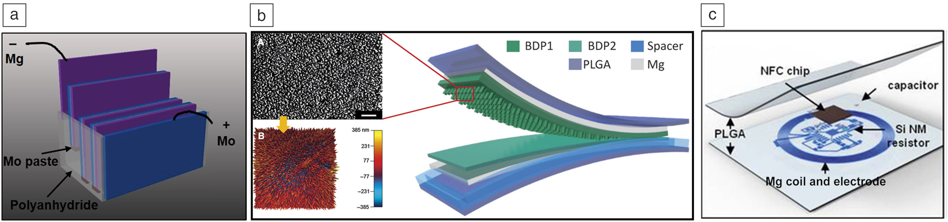
Figure 2. Schematics of transient energy devices. (a) Battery with four stacking Mg-Mo cells in series. Adapted with permission from Reference 27. © 2014 Wiley. (b) Mechanical energy harvester using triboelectricity. Scale bar = 10 um. Adapted with permission from Reference 29. © 2016 AAAS. (c) Wireless energy transfer with near-field inductive coupling. Adapted with permission from Reference 2. © 2016 Springer Nature. Note: PLGA, poly(lactic-co-glycolic acid); NFC, near-field communication; BDP, biodegradable polymer.
Energy harvesters that convert physical energy into electrical energy can also be used as transient energy sources. Figure 2b shows several examples of transient energy harvesters. A representative energy harvester has been suggested using biodegradable and piezoelectric metal oxide, ZnO with biodegradable Mg electrode, and silk substrates.Reference Dagdeviren, Hwang, Su, Kim, Cheng, Gur, Haney, Omenetto, Huang and Rogers33 As a mechanical energy harvester, this device generates ∼0.55 nA current, ∼1.14 V output voltage, and ∼10 nW/cm2 power density with 0.28% energy-conversion efficiency. A recent study explored another type of mechanical energy harvester, a triboelectric generator: the friction between two different biodegradable polymers such as PLGA, PVA, PCL, and PHB/V can generate a power of 32.6 mW/m2.Reference Zheng, Zou, Zhang, Liu, Shi, Wang, Jin, Ouyang, Li and Wang34
Device size, life span, and energy densities remain key issues in batteries and various energy harvesters for biodegradable applications where miniaturization, long-term operation, and sufficient power are critical. Wireless transmitting power using near-field inductive coupling has been proposed as an alternative to implantable transient devices. The effectiveness of this type of energy transfer has been verified by recent biomedical applications in wireless hyperthermia to minimize residual bacteria after surgery, electrical stimulation to accelerate peripheral nerve regeneration, and heat modulation to control drug delivery.Reference Kang, Murphy, Hwang, Lee, Harburg, Krueger, Shin, Gamble, Cheng, Yu, Liu, McCall, Stephen, Ying, Kim, Park, Webb, Lee, Chung, Wie, Gujar, Vemulapalli, Kim, Lee, Cheng, Huang, Lee, Braun, Ray and Rogers2,Reference Yu, Kuzum, Hwang, Kim, Juul, Kim, Won, Chiang, Trumpis, Richardson, Cheng, Fang, Thomson, Bink, Talos, Seo, Lee, Kang, Kim, Lee, Huang, Jensen, Dichter, Lucas, Viventi, Litt and Rogers3,Reference Lee, Kim, Harburg, Park, Ma, Pan, Kim, Lee, Kim, Jang, Kang, Huang, Kim, Lee, Leal and Rogers5 Figure 2c shows wireless power and data transmitting devices using inductive coupling for wireless monitoring of intracranial pressure.Reference Kang, Murphy, Hwang, Lee, Harburg, Krueger, Shin, Gamble, Cheng, Yu, Liu, McCall, Stephen, Ying, Kim, Park, Webb, Lee, Chung, Wie, Gujar, Vemulapalli, Kim, Lee, Cheng, Huang, Lee, Braun, Ray and Rogers2
The article by Jia et al. summarizes transient energy sources, focusing especially on energy-storage devices from batteries to supercapacitors.Reference Jia, Wang, Lee, Yu and Wallace26
Triggered transient electronics for active lifetime control
The lifetimes of most eco-/bioresorbable or water-soluble forms of transient electronics are, as previously described, passively determined by the selection of constituent materials and system geometries, where ambient conditions (e.g., pH, temperature, and ionic content of the surrounding aqueous environments) dictate the overall dissolution kinetics. Advanced approaches, sometimes referred to as triggered transience,Reference Hernandez, Kang, Lee, Hwang, Kaitz, Inci, Park, Chung, Sottos, Moore, Rogers and White7–Reference Lee, Jeong, Liu, Zhang, Shi, Kang, Kim, Kim, Lee, Kim, Jang, Yin, Kim, Banks, Paik, Huang and Rogers10 make possible deterministic, active control over the initiation of dissolution, disintegration, depolymerization, or other chemical or physical processes. Such capabilities can be exploited in biomedical devices to allow the release of drugs at specific intervals or in military systems to enable destruction of secured hardware upon recovery by an adversary. Several studies illustrate on-demand, fast, and accurate control over the behavior of transient electronics with diverse materials systems, device structures, and trigger stimuli.
Figure 3a shows an example of triggering in which disintegration of a supporting substrate of cyclic poly(phthalaldehyde) (cPPA) occurs upon exposure to light.Reference Hernandez, Kang, Lee, Hwang, Kaitz, Inci, Park, Chung, Sottos, Moore, Rogers and White7 Here, the cPPA contains 2.5–5% of 2-(4-methoxystyryl)-4,6-bis(trichloromethyl)-1,3,5-triazine (MBTT) as a dopant that yields photoactivated reactive Cl· radical species and hydrochloric acid (HCl), to cleave the acetal backbone of the cPPA. Exposure to UV light (λmax = 365 nm) initiates depolymerization of the cPPA, leading to the disintegration of the ultrathin electronic components on the substrate.

Figure 3. Triggered transient electronics for active lifetime control. (a) Photoinitiated transiency of 2-(4-methoxystyryl)-4,6-bis(trichloromethyl)-1,3,5-triazine (MBTT)/cyclic poly(phthalaldehyde) (cPPA) substrate with electronics. Adapted with permission from Reference 7. © 2014 Wiley. (b) Transiency of acid-sensitive substrates (cPPA) and circuit (Mg) by release of methanesulfonic acid dispersed in wax encapsulation initiated by heat melting. Adapted with permission from Reference 9. © 2015 Wiley. (c) Structure of mechanical destruction of electronics by using an expandable polymer. Adapted with permission from Reference 8. © 2017 Wiley. (d) Wireless microfluidic device with thermal expansion polymer, and series of images showing the selective and sequential injection of water with dye by heat triggering the expandable polymer. Adapted with permission from Reference 10. © 2014 Wiley.
Thermal triggering mechanisms provide a complementary set of opportunities. In one example, metastable substrates such as cyclododecane (C12H24) sublime under ambient conditions; this accelerates at elevated temperatures to induce disintegration of the supported electronics.Reference Yoon, Lee, Choi, Lee, Kim, Kim, Moon, Lim, Kim and Choi35Figure 3b shows further examples of triggering by thermal means, where advanced chemistries allow additional flexibility.Reference Park, Kang, Hernandez, Kaitz, Wie, Shin, Lee, Sottos, Moore, Rogers and White9 Park et al. describe a wax with 3% methanesulfonic acid introduced by stirring at 70°C; upon melting, rapid degradation of acid-sensitive metal interconnect lines (i.e., Mg) and substrate (i.e., cPPA) occurs by chemical etching.Reference Park, Kang, Hernandez, Kaitz, Wie, Shin, Lee, Sottos, Moore, Rogers and White9 A radio-frequency approach allows wireless delivery of thermal power for remote triggering.
Other strategies rely on the thermal expansion of polymers to fracture the essential components of electrical circuitsReference Gumus, Alam, Hussain, Mishra, Wicaksono, Sevilla, Shaikh, Diaz, Velling, Ghoneim, Ahmed and Hussain8 or to cause the release of active liquid species from microfluidic reservoirsReference Lee, Jeong, Liu, Zhang, Shi, Kang, Kim, Kim, Lee, Kim, Jang, Yin, Kim, Banks, Paik, Huang and Rogers10 for chemical reactions or pharmacological delivery. As an example of the former, Figure 3c shows the instant destruction of a device on a thermally expandable polymer (Expancel 031 DU 40, AkzoNobel) composed of polymeric microspheres that encapsulate small amounts of liquid hydrocarbon.Reference Gumus, Alam, Hussain, Mishra, Wicaksono, Sevilla, Shaikh, Diaz, Velling, Ghoneim, Ahmed and Hussain8 When an integrated thermal actuator reaches temperatures above 80°C, the polymer expands irreversibly by nearly 10 times due to a phase change of the hydrocarbon from liquid to gas. Figure 3d shows a microfluidic system that releases etchants upon heating of a polymer beyond a critical level.Reference Lee, Jeong, Liu, Zhang, Shi, Kang, Kim, Kim, Lee, Kim, Jang, Yin, Kim, Banks, Paik, Huang and Rogers10 Water and sodium hydroxide act to dissolve Mg (Mg + 2H2O → Mg(OH)2 + H2) and Al (2Al + 2NaOH + 2H2O → 2NaAlO2 + 3H) electrodes, respectively, thereby destroying an antenna by etching.
The article by You et al. surveys strategies in triggered transient electronics to initiate degradation or terminate device function on demand via various stimuli.Reference You, Zhao, Guo and Mei27
Outlook
Transient electronics research has seen explosive recent expansion in the discovery and analysis of water-soluble or degradable materials, and demonstrations of versatile devices for applications. The potential of transient electronics and the possibility of translation to applications relevant and useful to society has been clearly demonstrated.
Moving forward, we believe that the following areas of materials research are necessary: (1) precise control of degradation and operational lifetime adjustment, (2) development of new classes of transient electronic materials to increase the choice of electronic and degradation properties and other functionality, and (3) evolution toward high-performance electronics to translate the techniques to industry.
Transient electronics require sophisticated efforts to reduce the gap between materials degradation and the functional lifetime of electronic devices. This gap arises from the quick diffusion of water molecules through the protective layer into the electronic circuit before the protective layer can dissolve out. Enhancing the water-barrier properties of encapsulation layers is critical for precise control of the functional lifetime without increased layer thickness or total degradation time. This requires understanding the dissolution kinetics of water-diffusion behavior and developing nanostructural or molecular approaches to control it. The surface modification of transient encapsulation, one potential solution, requires understanding the surface chemistry at the molecular level to control the interaction between water molecules and the surface. Work on forming extremely dense encapsulation structures is also essential to slow down vapor diffusion into the layer. All of these considerations must be explored in transient passive materials, and the fields under consideration will no doubt expand.
The choice of electronic materials in transient electronics is limited to some inorganics and polymers whose dissolution chemistry and kinetics are known, especially at this new thickness scale. There are still great opportunities to discover new water-soluble or biodegradable electronic components that are electrically conductive and have semiconducting and dielectric properties. This effort can be furthered by exploring new classes of metal alloys with biodegradable components, designing nanostructured materials with transient metal and metal oxides, and synthesizing new types of polymers. Composites of transient inorganics and polymers are another great option. This will enrich the design choices for electronic devices by consideration of various electrical, transient, mechanical, and other properties.
In another direction, current techniques must be translated to industry so that they can influence medical practice. The first step will be moving forward to chip-scale devices made by reliable, high-performance processing. Most current demonstrations of transient electronics remain in the realm of materials development with one or two simple functional operations. Designing and developing chip-scale devices will be the first step toward the sophisticated transient devices with extensive performance and applications. Continuous efforts must be made to find materials and fabrication methods that are compatible with industrial processes. Extensive research in this translation stage should also explore the materials issues and reliability problems that will arise in stacking and packaging such chips
The articles in this issue not only summarize and overview recent developments in transient electronics in representative fields, they also offer information, suggestions, and ideas for the next generation of transient electronics devices.

Seung-Kyun Kang has been an assistant professor in the Department of Materials Science and Engineering at Seoul National University, Republic of Korea, since 2019. He was an assistant professor in the Department of Bio and Brain Engineering at the Korea Advanced Institute of Science and Technology, Republic of Korea, from 2017 to 2019. He obtained his BS and PhD degrees in materials science and engineering from Seoul National University, in 2006 and 2012, respectively. He was a postdoctoral researcher at the University of Illinois at Urbana-Champaign from 2012 to 2016 and at Northwestern University from 2016 to 2017. Kang can be reached by email at kskg7227@snu.ac.kr.

Lan Yin is an associate professor in the School of Materials Science and Engineering at Tsinghua University, China. She received her bachelor’s degree from Tsinghua University in 2007, and her PhD degree from Carnegie Mellon University in 2011. She was a postdoctoral researcher at the Massachusetts Institute of Technology from 2011 to 2012 and the University of Illinois at Urbana-Champaign from 2012 to 2015. Yin can be reached by email at lanyin@tsinghua.edu.cn.

Christopher Bettinger is a professor at Carnegie Mellon University (CMU) in the Departments of Materials Science and Engineering and Biomedical Engineering. He directs the laboratory for Biomaterials-Based Microsystems and Electronics at CMU, which designs materials and interfaces to integrate medical devices with the human body. He is also a co-inventor on several patents and co-founder and chief technology officer of Ancure, an early-stage medical device company. He received his SB degree in chemical engineering, his MEng degree in biomedical engineering, and his PhD degree in materials science and engineering, all from the Massachusetts Institute of Technology, where he was a Charles Stark Draper Fellow. He completed his postdoctoral fellowship at Stanford University in the Department of Chemical Engineering, where he was a National Institute of Health Ruth L. Kirschstein Fellow. Bettinger can be reached by email at cbetting@andrew.cmu.edu.


