

Graphene’s hexagonal honeycomb lattice leads to a band structure that can be represented by two cones that touch at and are symmetric about the Dirac energy. Single-layer graphene therefore has a zero bandgap and the electrons and electron holes have the same properties. With no bandgap, however, it is difficult to control the electrical conductivity of graphene and opening of a tunable bandgap would represent a significant step forward in exploiting graphene in electronic and photonic applications.
One approach to achieving a bandgap is through the use of materials consisting of crystallographically stacked layers of graphene. While a bandgap has been induced in AB-stacked bilayer graphene through application of a perpendicular electric field, this does not occur in typical trilayer graphene, which exhibits ABA, or Bernal stacking, due to its mirror symmetry (see Figure 1a). The recently discovered rhombohedral trilayer graphene, which has ABC stacking (see Figure 1b), has, however, been predicted to exhibit an induced bandgap.
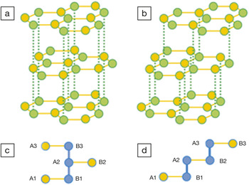
Figure 1. Crystal structures are shown for (a) ABA and (b) ABC trilayer graphene. The yellow and green atoms represent the A and B sublattices of the graphene honeycomb structure, respectively. Tight-binding diagrams are shown for (c) ABA and (d) ABC trilayer graphene. Effective interlayer coupling vanishes at the K-point, so that the yellow atoms become non-bonding monomers. The blue atoms then form a trimer in the ABA trilayer, but in the ABC trilayer they form two dimers. Reproduced with permission from Nature Physics (DOI: 10.1038/nphys2102). © 2011 Macmillan Publishers Ltd.
Now, T.F. Heinz and co-researchers from Columbia University along with E. Capelluti from the Institute for Complex Systems, Italy, and Instituto de Ciencia de Materiales de Madrid, Spain, have used theory and experiment to demonstrate bandgaps as large as 120 meV in ABC-trilayer graphene.
As reported in the September 25 online edition of Nature Physics (DOI: 10.1038/nphys2102), the researchers investigated graphene trilayer samples from exfoliated kish graphite (a nearly ideal crystal precipitated from molten iron) on SiO2/Si substrates. Infrared and Raman spectroscopy was used to sample thickness and stacking order. For both ABA and ABC trilayer graphene samples, the researchers induced high doping densities and electric fields in the samples with an electrolyte top gate, and monitored the band structures with infrared conductivity measurements.
The researchers observed no signature of bandgap opening for ABA trilayer graphene, while, for similar electric fields, a sizable bandgap of 120 meV was observed for the ABC trilayer. The implications of the different crystal structures of the two trilayers were demonstrated with tight binding calculations that accounted for interlayer coupling and the capacitance of the electrolyte top gate.
Representing the ABA trilayer by one trimer and three monomers (see Figure 1c), the researchers showed that although a vertical electric field lifts the degeneracy of the two monomer states on the bottom and top layers, it influences neither the middle-layer monomer state nor the non-bonding trimer state. This remaining degeneracy precludes bandgap induction.
In contrast, the ABC trilayer is represented by two dimers with finite energies and two monomers with zero energy (see Figure 1d), so that application of a perpendicular electric field results in different potentials at the bottom and top layers. This lifts the degeneracy of the two monomers and induces a bandgap.
The researchers said, “Our work suggests that a tunable bandgap can be induced in thicker graphene samples with ABC (rhombohedral) stacking order, thus providing a still broader class of materials with a tunable bandgap.”

