

Research is being conducted to employ wide-bandgap semiconductors such as SiC, GaN, and diamond to replace silicon to overcome its inherent limitations of high-frequency switching and power handling. Now researchers at the National Institute for Materials Science (NIMS) in Japan have designed a diamond-powered transistor that can be used in extreme environmental conditions like harsh temperatures and radiation conditions, as reported in a recent issue of IEEE Electron Device Letters (doi:10.1109/LED.2017.2702744). Due to their high power frequency, thermal limits, and low power loss at high frequency, diamond-based electronic devices outshine other wide-bandgap semiconducting materials-based devices.
In this study, the researchers used a microwave plasma-enhanced chemical vapor deposition technique to grow a 150-nm-thick epitaxial layer of hydrogenated diamond (H-diamond) at 900–940°C with a chamber pressure of 80 Torr. A 4-nm-thick layer of Al2O3 was selected as a buffer (to reduce the effect of lattice mismatch) for the LaAlO3 to utilize H-diamond in enhancement-mode metal oxide semiconductor field-effect transistor (MOSFET) architecture, and a 30.4-nm-thick layer of Al2O3 was deposited on H-diamond for the operation of depletion-mode MOSFETs. Both types of devices were completed with Ti/Au metal deposition through e-beam evaporation. The schematic diagram of both circuits is shown in the Figure.
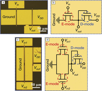
Top views (a,c) and schematic diagrams (b,d) of the H-diamond metal oxide semiconductor field-effect transistor NOT and NOR logic circuits, respectively. The V in , V out , and V DD represent input voltage, output voltage, and supply voltage, respectively. The V in1 and V in2 represent two input voltages for the NOR logic circuits. E-mode is enhancement mode and D-mode is depletion mode. Credit: IEEE Electron Device Letters.
An increase in gain maximum for the NOT logic circuit from 1.2 to 26.1 was recorded when the voltage supplied was changed from –5.0 to –25.0 V. The NOR logic circuit configuration showed immaculate NOR gate characteristics. According to Jiangwei Liu of NIMS, “The fabrication of logic circuits will push forward the development of diamond MOSFET current switches and digital circuits for high-temperature, high-power, high-frequency, energy-saving, and low-carbon practical applications.”
“Enhancement mode (normally-off) is useful for diamond FET,” says Hiroshi Kawarada from Waseda University. According to Kawarada, the research team should move toward high-temperature operation and record the radiation hardness of circuits. He adds, “It is really useful for the safe dismantling of nuclear reactors and taking out the debris.” Yasuo Koide, vice president at NIMS, anticipates that these diamond-powered transistors will be commercialized for general applications in about 10 years. “However, in the limited field of radiation in the nuclear plant and space applications, the devices will be commercialized within five years,” Koide says.
Liu believes that this is just the beginning and he would like to take his research in the direction of stable devices even at high temperatures. Currently, the diamond-based devices do not perform well if the operating temperature is above 300°C. He says, “The final target of my study is that the H-diamond-based devices such as NOR, NOT, NAND, and the ring oscillator can operate stably at more than 500°C.” The roadmap for these advancements, he says, are “(a) to change the fabrication process, (b) to find a good ohmic contact metal to H-diamond, (c) to treat the H-diamond surface using plasma, and (d) to change the deposition conditions for the oxide insulator.”
