


Introduction
Radiation damage in the transmission electron microscope (TEM) has been a problem ever since researchers in the late 1940s put organic specimens into the electron beam, hoping to see details beyond the limit of a light microscope, or even processes occurring within living cells. But as in the initial studies of radioactive materials or the first atom-bomb tests, there was little recognition of the damaging effect of ionizing radiation. This process starts with the breaking of chemical bonds, causing structural damage on an atomic scale (observable from TEM diffraction patterns), and leads to longer-range disruption of structure (seen in TEM images) and the removal of some chemical elements (known as mass loss, measurable by energy-loss or x-ray spectroscopy).
With the development of brighter electron sources, improved aberration-corrected optics, and better electron detectors, damage has emerged as an important limiting factor in many areas of electron microscopy.
Electron-beam damage has many aspects, as described in a recent review paper [Reference Egerton1], and what follows is, in part, an update to that article, collecting together various mathematical formulas and references to recent publications. From time to time, people find new ways of using electron beams to fabricate small structures, so that creative aspect of radiation damage will also be discussed briefly.
Radiation Effects in an Electron Microscope
An electron beam can cause permanent change to a TEM specimen (thickness t) through several physical mechanisms as discussed below.
Heating.
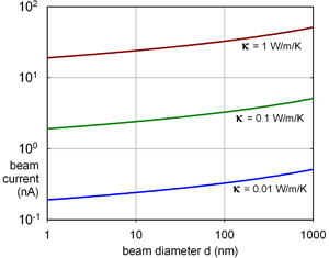
Within the irradiated volume (radius R), inelastic scattering generates heat that is removed by conduction (for example, to an annular heat sink at distance R 0 away). For a specimen of density ρ and specific heat C p, the temperature rise is exponential with a time constant τh = R 2 ln(R 0/R) [ρC p/(2κ)], typically 1 ps for a small probe of diameter 2R = 1 nm. The final temperature rise is ΔT ~ IbE m(eV) ln(R 0/R)/(2πκλi), where E m (~ 7Z for atomic number Z < 30) is the mean energy loss per inelastic collision, λi is the inelastic mean free path, and κ is the thermal conductivity of the specimen. For most materials, κ > 0.1 W/m/K at room temperature and ΔT does not exceed 10 K for beam currents typical of a modern TEM (Figure 1) so thermal decomposition cannot account for most damage observations. However, polymers such as polystyrene (with κ ~ 0.01 W/m/K at T = 100 K) can soften and fall apart in the beam, assisted by forces due to electrostatic charging. With the condenser aperture removed, thermionic-source TEMs have allegedly generated beam currents high enough to melt metallic specimens.
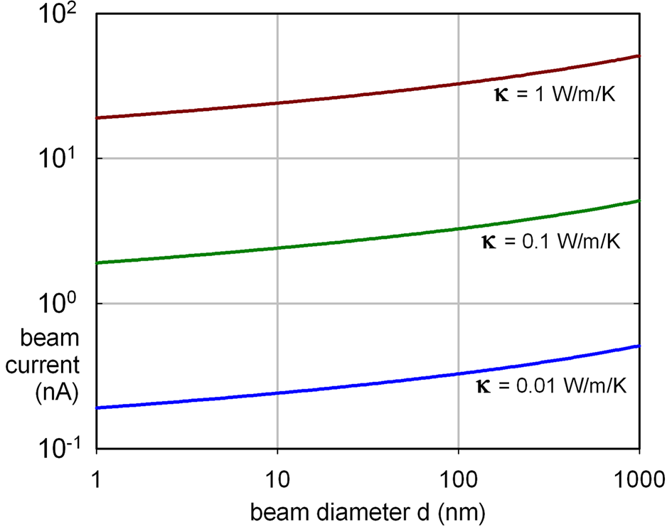
Figure 1: Beam current (in nA) giving ΔT = 10 K for specimens of thermal conductivity κ, calculated assuming E m = 40 eV, λi = 100 nm, R 0 = 30 µm.
Charging
Inelastic scattering causes emission of secondary and Auger electrons, creating a local charge Q, a radial conduction current I c, and an increasing surface potential V s that reduces the total yield Y(V s) from each surface (Figure 2). This charge accumulation has an RC time constant τq = (V s/I c)(Q/V s) = ε0εr/σ that depends on the electrical conductivity σ and permittivity εr of the sample, but not on the beam current or radius. For a poor-quality insulator, the result may be a steady-state condition: I c = I bY(V s), with V s = I b Y(V s) ln(R 0/R)/(πσt) and a charge density within the irradiated volume given by ρe = Q/(πR 2t) = 2ε0εr I b Y(V s)/(πσtR 2). The voltage gradient is highest at the edge of the probe: dV/dr = V s/[R ln(R 0/R)].
Figure 2: Left, radial heat flow from the irradiated volume of specimen (radius R) to a heat sink at distance R 0. Right, electron current arising from emission of secondary and Auger electrons, creating a surface potential V s and accumulated charge Q.
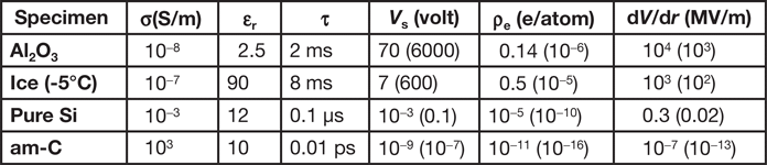
Table 1 shows estimates based on these macroscopic formulas, taking t = 100 nm, R 0 = 30 µm, and Y(V s) = 10−2, for a STEM probe (2R = 1 nm, I b = 0.4 nA) and for TEM illumination (2R = 5 µm, I b = 100 nA, values given in parentheses). The charge density ρ is given in terms of electron units per atom.
Table 1: Charging calculated assuming classical electrostatics and ohmic conduction.
Radiolysis.
Inelastic scattering causes ionization damage (radiolysis): the breakage of chemical bonds and loss of atomic structure followed by ejection of atoms from the sample (mass loss). For an incident beam with uniform current density, the TEM signal (for example, diffracted-peak intensity) is often proportional to exp(-D/D c), where D is the electron dose (product of current density and exposure time) and D c is a critical or characteristic dose, dependent on the accelerating voltage and specimen temperature. For a non-uniform beam, the decay is no longer exponential (Figure 3).
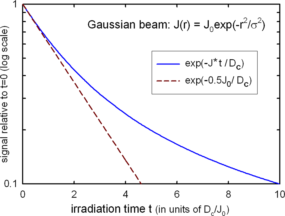
Figure 3: Damage response for a Gaussian or a diffraction-limited probe (blue curve) compared with the exponential decay calculated for a current density equal to half the peak value.
Radiolysis in an organic specimen is reduced (by a factor of typically 2 to 20) by cooling to around 100oK, supposedly by suppressing the diffusion of radiation-induced reaction products (single atoms, radicals, ionized species). Chemical scavengers such as antioxidants may also curtail structural damage at room temperature [Reference Kuei and Gomez2], but not at 100oK where diffusion is already largely eliminated. Encapsulation in ice or between layers of carbon is found to reduce damage and is employed in cryo-EM (together with cooling) to permit structural measurements on proteins and other important biological molecules [Reference Henderson and Russo3].
Any substantial heating effect of a beam will increase the radiation sensitivity, giving a direct dose-rate effect (D c falling with increasing dose rate). Conversely, mass transport and associated structural damage may be diffusion-limited, giving an inverse response (Figure 4).
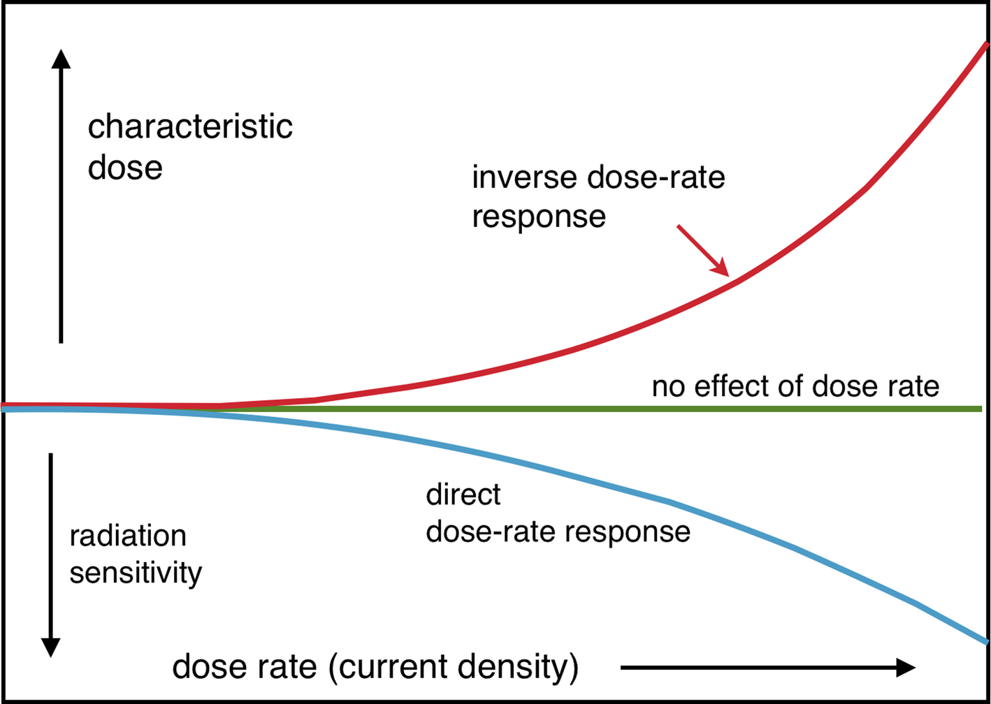
Figure 4: Possible dose-rate effects: direct (due to heating or charging) and inverse (arising from diffusion limits).
Knock-on damage.
High-angle elastic scattering causes knock-on displacement of individual atoms of the specimen. This process is inefficient, so it is most commonly observed in metals and semiconductors where radiolysis is absent. The interaction is highly localized and has been used to produce changes on an atomic scale [Reference Krasheninnikov and Banhart4]. There is evidence that inelastic scattering can supply some of the energy needed for displacement of a particular atomic species, allowing modification at primary-beam energies below the threshold value calculated from relativistic kinematics [Reference Kretschmer5].
STEM versus TEM for Radiation-Sensitive Specimens
A question of longstanding concern is how much damage scanning transmission electron microscopy (STEM) produces, relative to TEM and for the same amount of retrieved information. Beam heating is less, but only because the current achievable in a small electron probe is much below that used for TEM imaging.
Charging effects are time-dependent and sensitive to dose rate, which is typically a factor of 103–105 higher in STEM. As seen in Table 1, the charging time for resistive specimens may exceed the pixel dwell time (0.16 μs for a 250 × 250 raster recorded in 10 s). The specimen would then discharge between adjacent frames if there were no charge trapping. Random or sparse sampling (as opposed to conventional raster scanning) might allow less charge accumulation and damage [Reference Stevens6]. A similar situation may apply to short-pulse beams [Reference VandenBussche and Flannigan7,Reference Jing8], except that Coulomb repulsion between beam electrons precludes sub-μm probes with very high current density [Reference Egerton9,Reference Spence10].
For good insulators, including most organic specimens, the electric field just outside a STEM probe well exceeds the breakdown strength (100–1000 MV/m), as seen in the last column of Table 1. Calculated assuming ohmic conduction, V s and ρ will then be overestimates, but local dielectric breakdown might itself be damaging. The charge density ρe is much higher in STEM mode and might even increase the amount of bond breaking; time-dependent density-functional calculations [Reference Cai11] can hopefully answer this question. Such an effect would lead to a direct dose-rate dependence of damage, the amount increasing above some current-density threshold that should increase with increasing primary energy due to the reduced secondary-electron and Auger yield.
In an inorganic oxide, the electrostatic field can give rise to ionic drift, resulting in phase segregation or phase transformation [Reference Jiang12] that could be worse in STEM mode. But STEM elemental mapping might benefit from diffusion limits (which reduce radiolytic mass loss) if fast-recording EELS and EDX detectors are available [Reference Egerton and Qian13].
Charging effects are reduced or eliminated (for example, in cryo-EM imaging of biomolecules) by coating the sample with a thin layer of amorphous carbon [Reference Glaeser and Downing14,Reference Glaeser15]. Graphene may work even better, as a conducting layer and diffusion barrier [Reference Algara-Siller16].
After irradiation by x-rays, dark progression of damage is sometimes observed [Reference Warkentin17]. If it turns out to be significant for electron irradiation of thin specimens, single-frame STEM acquisition would be advantageous [Reference Egerton and Qian13].
Increasing signal-collection efficiency is just as important as reducing damage. Phase-contrast provides the largest signal from light-element samples and has traditionally been carried out using fixed-beam TEM mode. But using recently developed algorithms and perhaps combined with ptychography, STEM might be capable of comparable or greater efficiency [Reference Krumeich18–Reference Ren22].
Consequences for Small-Probe Fabrication
Ultraviolet lithography is the basis of microelectronics fabrication and relies on the radiolysis of organic “resists” for patterning. Electron-beam lithography can utilize the same resists but is carried out serially using a focused electron beam. A 50 μC/cm2 dose of 20 keV electrons is said to reduce the molecular weight of 70% of PMMA molecules, crosslinking about 2% of them [Reference Wilkinson, Beaumont, Kelly and Weisbuch23]. Αfter chemical development of the latent image, linewidths down to 20 nm are achievable [Reference Wilkinson, Beaumont, Kelly and Weisbuch23], or below 10 nm with 200 kV aberration-corrected optics [Reference Manfrinato24]. For a sensitive resist, there is always a statistical limit to spatial resolution due to the small number of beam electrons producing the damage [Reference Crozier25]. The resolution of organic polymers may also be limited by their large molecular size [Reference Broers26], which has provided an incentive for using smaller molecules.
A focused field-emission probe has been used to create holes of 1–5 nm diameter in metal halides [Reference Muray27] and oxides [Reference Salisbury28,Reference Hollenbeck and Buchanan29]. If used as a self-developing resist that volatilizes during exposure, these inorganic materials avoid the need for wet-chemical processing. Each hole could represent one bit of stored information, the small dimensions enabling high information density, but the sensitivity is well below that of organic resists (Table 2). It may be true that the Encyclopedia Britannica could have been written on a pinhead [Reference Humphreys30], but that procedure would have taken at least a year.
Table 2: Approximate values of the dose D, hole diameter d, time to write 106 holes, and the damage mechanism for material removal by a beam (1 nm diameter, current 0.4 nA) of 200 keV electrons.
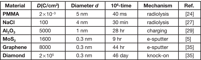
Organics and halides may damage by radiolysis, but hole drilling in amorphous alumina appears to involve electrostatic charging, as suggested by the existence of a threshold current density. If the charge density ρe exceeds about 0.1 e/atom, interatomic repulsion causes a Coulomb explosion, and ions are emitted from the specimen surfaces [Reference Cazaux31].
Any damage process that depends on inelastic scattering is limited in resolution by the long-range nature of the electrostatic interaction between beam and atomic electrons (Coulomb delocalization). Another fundamental limit arises from lateral motion of the secondary electrons, which cause most of the damage in organic materials [Reference Wu and Neureuther32]. As a result of these two effects, it appears that about 50% of the energy is deposited outside a 1 nm diameter probe [Reference Egerton33,Reference Egerton and Malac34].
These limits are avoided by basing the fabrication on knock-on displacement of individual atoms, the only damage process in electrically conducting materials. For thicker samples and high incident energies, knock-on means displacement of lattice atoms to interstitial sites. But for 2D materials (for example, MoS2, graphene) and lower energies, the displacement is predominantly electron-beam sputtering of surface atoms. Both processes are included in Table 2, which illustrates the limitation on writing speed that results from the low probability of high-angle elastic scattering.
Conclusions
Radiation damage is a curse for electron microscopy of beam-sensitive specimens but a blessing for electron-beam fabrication, which could result in devices far smaller than those possible with UV light. Progress in our understanding has been slow, but time-dependent quantum calculations and further advances in experimental technique should lead to improved control over the damage process.


