Introduction
Aberration-corrected transmission electron microscopes (TEMs) and scanning transmission electron microscopes (STEMs) are the state-of-the-art microscopes for a TEM laboratory nowadays. In the past few years, with the integration of aberration-corrected electron optics, notably the CEOS GmbH aberration corrector [Reference Rose1] into commercial TEMs and the Nion corrector [Reference Nion2] into commercial STEMs, capabilities such as sub-Ångstrom resolution imaging and chemical mapping at the atomic level have become possible.
Florida State University (FSU) recently installed a probe aberration-corrected cold field-emission JEOL JEM-ARM200cF TEM, boosting its materials characterization capabilities to a new level. With a specially constructed microscope room, we can achieve high performance routinely. More details about this microscope have been reported elsewhere [Reference Xin3]. Advanced imaging and spectroscopy techniques are available on our JEM-ARM200cF. This article describes our instrument, our installation, and some results.
Microscope Room Details
Since the availability of the aberration-corrected microscope, the importance of the room environment on the performance of high-end instruments has been recognized in many laboratories. A quiet TEM room with low electromagnetic stray fields, low floor vibration, low acoustic noise, and low temperature drift is essential for achieving expected performance [Reference Muller4, Reference O’Keefe5].
Before the arrival of the microscope, we surveyed several potential sites, and the best location was chosen from several available spaces. Subsequently, a new TEM lab was designed and built inside the National High Magnetic Field laboratory (NHMFL) building (Figure 1a). The TEM lab layout is shown in Figure 1b, with a remote operation/sample loading room and a separate utility room that houses the power supplies for the microscope and the CEOS corrector.

Figure 1 The electron microscopy facility at Florida State University. (a) An aerial view of the National High Magnetic Field Laboratory from the Google map. The microscope room location is at the corner of the building, indicated by a red circle. (b) TEM laboratory layout sketch showing the location of the different rooms. (c) Microscope room after installation. (d) Sample loading/remote operation room.
The microscope room was purposely designed to minimize electromagnetic stray fields, acoustic noise, vibrations, and temperature variations. The foundation of the room was constructed with 6.1 m × 5.5 m concrete floor slab at 1 m thick. The slab was isolated from the remainder of the building’s foundation with a 5 cm foam gap. A room within a room was built on this isolated slab inside the outer wall of the NHMFL building. The microscope room wall is 15.2 cm thick, made of sheetrock reinforced with metal studs filled with fiberglass batts. The single-story building has a standing seam metal roof with a concrete deck, beneath which a suspended ceiling was hung. One double door for maintenance purposes and one single door for daily entrance are made of hollow steel and are filled with a material having a sound transmission class rating of 50. The interior walls of the room are covered with twenty-two 5.08 cm thick, 283 × 60 cm2 fabric-covered fiberglass sound-absorbing panels.
Room temperature and airflow control are accomplished by a combination of cooling radiant panels and an air handler. Eighteen radiant panels (Energie Solaire SA, Switzerland), each with an area of 1.88 m2, were installed on the walls above the acoustic panels. The room air is recirculated with a constant exhaust and resupply of 50 cubic feet per minute sourced from the main building air conditioning system, which has already been dehumidified. The air handling duct system consists of a duct silencer on the inlet and outlet of the air handler to minimize transmission of fan noise into the room. Inside the room, two fabric diffusers from DuctSox were mounted on the ceiling to evenly and quietly bring air into the space.
To minimize electromagnetic stray fields, several precautions were made. Water chillers for the microscope and the cooling panels are located 50 m away from the microscope room. All AC wiring entering or near the room was twisted greater than 4 times per foot. All of the supporting electrical equipment was installed in an adjacent room. The uninterrupted power system (UPS) was installed in a remote electrical room in the building.
Figure 1(c) shows the finished room with the JEM-ARM200cF installed. The room environment was measured to be within the required noise level for the installation. Figure 2 shows electromagnetic field and floor vibration measurements of the finished room. The detected AC field at 60 Hz was well below 0.3 mG, and the DC field was below 0.1 mG. Only two vibration peaks close to 10 Hz along one direction are higher than the requirement, but we did not find this generated any noise in the STEM images. In fact, we do not detect interferences from any outside noise/disturbance.
Figure 2 Diagrams of electromagnetic stray field and vibration measurement of the finished microscope room. (a) A typical AC electromagnetic field measured of the room. The 60 Hz stray field comes from the electrical and lighting systems outside the room. (b) A diagram of the measured DC electromagnetic field. (c) and (d) show floor vibration measurements along two horizontal directions. All vibration frequencies are below required specifications, except the two peaks close to 10 Hz.
Microscope and Auxiliary Equipment
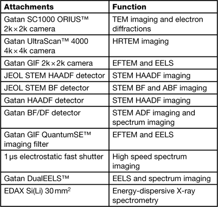
The FSU microscope has a CEOS CESCOR hexapole aberration corrector (CEOS GmbH) for the probe forming lenses. Table 1 lists the detectors and image recording devices with their corresponding functions.
Table 1 A list of auxiliary attachments on Florida State University’s JEM-ARM200cF.
The microscope can work in either TEM or STEM modes at 200 kV, 120 kV, and 80 kV. Once aligned, it is easy to switch between TEM and STEM mode without any adverse effects on the alignment or image resolution, which makes it convenient to study materials by different techniques. The TEM sample stage can be controlled by piezo-activators along the x, y, and z axes. In particular, the operator can locate and tilt the sample to a region of interest in TEM mode and switch to STEM mode for in-depth studies of the same region.
The microscope can be operated from the computer in the adjacent control room (Figure 1d) or from a remote computer. It is possible for distant users to watch actual operations or even operate the microscope via the internet.
Microscope Performance
The most important specifications of this microscope are the ultimate STEM image resolution, the electron energy resolution, and the high current density of the electron probe for analytical work. All the data shown here were acquired on this microscope at FSU after completion of the installation. The experimental images are original data without any image processing or filtering. The manufacturer’s standard resolution specification verification for STEM imaging uses a two-dimensional fast Fourier transform (FFT) pattern of the Si sample images, where the smallest d-spacing diffraction spots shown in the pattern indicate the resolution. The ultimate STEM resolution of this microscope is illustrated in Figures 3a to 3d. Figure 3a is a STEM high-angle annular dark-field (HAADF) image of Si [110]. Figure 3b shows its FFT pattern with the smallest d-spacing {444} diffraction spots (circled), confirming information transfer to 0.0784 nm (Si lattice parameter a = 0.5431 nm). In addition, the STEM HAADF image of Si [112] shown in Figure 3c demonstrates the STEM resolution in real space. The intensity line profile (Figure 3d) of the atomic column dumbbells shows an average valley-to-peak intensity of 71%. This satisfies the Rayleigh criterion of an 81% valley-to-peak ratio, where the separation of the Si atomic columns of 0.078 nm is apart. The flat region in the aberration-corrected Ranchigram from an amorphous carbon film (Figure 3g) has a 46.16 mrad convergence angle, confirming the sub-Ångstrom probe size.
Figure 3 Measured microscope specifications: (a) STEM HAADF image of Si [110] using the smallest probe size with corresponding FFT of the image (b). The circled diffraction spots are {444} of 0.078 nm. (c) STEM HAADF image of Si [112] using the smallest probe size. (d) Intensity line profile of the Si atoms of (c). (e) STEM HAADF image of Si [110] using high current density probe with corresponding FFT (f). The circled diffraction spots are {333} of 0.105 nm. (g) Ranchigram from amorphous carbon film showing the large flat region. (h) Zero-loss peaks showing the electron spectrometer energy resolution at full emission (0.46 eV) and at 1 µA (0.34 eV).
Electron probe with high current intensity is required for electron energy loss spectrometry (EELS) and energy dispersive X-ray spectrometry (EDS) chemical analysis characterization. For our microscope, the smallest probe size with adequate probe current for chemical analytical work is formed by choosing the “4c” probe size setting and a CL aperture of 40 µm, producing a probe current about 300 pA. Figure 3e is a STEM HAADF image of Si [110] using this probe, and the smallest d-spacing of the FFT (Figure 3f) is 0.105 nm for the {333} spots. This illustrates the image resolution for a high current density analytical probe. As shown in Figure 3h, at full emission current of 14.5 µA, the measured energy resolution of this microscope is 0.46 eV. Our highest recorded energy resolution was 0.34 eV, obtained with an emission current of 1 µA after the cold field-emission tip had been freshly flashed.
Results
Two important STEM techniques for a modern analytical microscope are STEM imaging and STEM spectrum imaging. STEM HAADF imaging is very powerful for imaging the atomic structure of materials because the image contrast is intuitive and straightforward. With aberration-corrected probe optics, we can easily and routinely acquire high signal-to-noise atomic resolution STEM HAADF images from different materials, as illustrated in the montage of images in Figure 4.
Figure 4 STEM HAADF images of different materials: (a) Twinned Au nano particle along [110]. (b) Fe2TiO4 along [110]. (c) WSe2 along [0001]. (d) Pr1.33Pt4Ga10 along [Reference Rose1–100]. (e) [100] Ba2IrO4/[001] SrTiO3 thin film. (f) Re doped NiMo alloy along [001].
STEM HAADF imaging requires a high inner angle on the annular detector so that the image intensity is proportional to Z n (n ~ 1.7 to 2) without coherent interference [Reference Hillyard and Silcox6, Reference Pennycook and Jesson7]. Heavy atoms usually show strong intensity whereas light atoms may produce an intensity too weak to be detected in STEM HAADF images. A new STEM imaging technique, annular bright-field (ABF) imaging, with a different image forming mechanism, allows even hydrogen atom columns to be observed [Reference Okunishi8] along with other heavy atoms. In the STEM ABF image, all the atoms show dark contrast on a bright background [Reference Findlay9, Reference Ryo10]. In the configuration of FSU’s JEM-ARM200cF, STEM HAADF and ABF images can be simultaneously acquired (Figure 5). Figure 5a shows the STEM HAADF Z-contrast image with collection angle from 76 mrad to 174 mrad, whereas Figure 5b shows the corresponding STEM ABF image of a double perovskite transition metal oxide Ba3MnNb2O9. The HAADF image shows the much brighter Ba atom columns (Z = 56) and the alternating intensities of the Mn (Z = 25) and Nb columns (Z = 41). An intensity profile of this atomic plane (inset) confirms the …Mn-Nb-Nb-Mn… ordering. The ABF imaging uses the diffraction range from 10.5 mrad to 21.6 mrad. The additional features between the Nb and Mn columns are oxygen atom columns. The STEM ABF imaging contrast is less sensitive to sample thickness and defocus than conventional high-resolution TEM images and promises to become an important technique for light-atom imaging.
Figure 5 (a) STEM HAADF image of a Ba3MnNb2O9 single crystal along [010]. Upper inset shows an enlarged image. Lower inset shows an intensity line profile along the smaller atomic plane showing the ordering of Mn-Nb-Nb-Mn-. (b) Corresponding STEM annular bright-field image. The oxygen atoms are indicated by arrows in the upper inset. Lower inset: Schematic of the unit cell structure projected along [010].
This microscope also provides a powerful analytical characterization technique, that is, chemical mapping via spectrum imaging, which collects and stores chemical and spatial information together. Figure 6 shows a STEM EELS mapping of GaAs/Ga2O3, demonstrating the best chemical mapping spatial resolution of this microscope. Figure 6a is the survey image for the spectrum imaging obtained using a probe size “4c” and a 40 µm condenser lens aperture with Gatan ADF detector. The GaAs dumbbells are clearly resolved with this high current density probe. The EELS data were acquired with a collection angle of 107 mrad. Figure 6b is the spectrum image with the size of 90 × 30 pixels, and each pixel was stored with an EELS spectrum (400 eV to 2400 eV) acquired with 10 ms exposure time. The extracted EELS spectra from GaAs and from Ga2O3 are shown in Figures 6c and 6d, respectively. The chemical maps (Figures 6e to 6h) were extracted using the multiple linear least square fitting (MLLS) routine available in Gatan DigitalMicrograph® [Reference Thomas11,Reference Longo, Twesten and Thomas12]. These maps demonstrate that we can achieve chemical mapping at atomic resolution.
Figure 6 Spectrum imaging of GaAs/Ga2O3 demonstrating the EELS analytical capability: (a) STEM annular dark-field survey image. The boxed region is the selected area for spectrum imaging. (b) Spectrum image of the boxed region. Each pixel contains an EELS spectrum. (c) and (d) extracted EELS spectra from boxed regions 1 and 2 in (b), showing the Ga L2,3, As L2,3, and O K core losses from GaAs and Ga2O3. (e) Atomic resolution As map. (f) Atomic resolution Ga map. (g) Oxygen map. (h) Colorized composite map showing Ga in green and As in red.
Figure 7 shows a STEM EELS map of [001] SrTiO3, illustrating the DualEELSTM capability of acquiring low-loss EELS and high-loss EELS simultaneously. The EELS spectrum imaging data were acquired from two regions simultaneously in DualEELSTM mode: the low-loss portion of the EELS spectrum of 0–2,000 eV at 54 µs/pixel and the high-loss region of 350–2,350 eV at 10 ms/pixel. The total acquisition time for the scanned area was 34 seconds. The extracted low-loss EELS spectrum (Figure 7c) from the low-loss spectrum image (Figure 7b) can be used to measure the thickness, to correct for plural scattering, and to obtain information available in the plasmon region of the EELS spectrum. Figure 7f is the thickness map of the scanned region. At the same time, the high-loss Sr L2,3 edges at 1940 eV (Figure 7e) can be collected with good signal-to-noise ratio. We can obtain the whole EELS spectrum for a wide energy range from 0eV to several thousand eV with the DualEELSTM mode, as shown in the spliced spectrum (Figure 7g). Atomic resolution Sr and Ti maps are shown in Figures 7h to 7J.
Figure 7 Spectrum imaging of [001] SrTiO3 with DualEELS™: (a) Survey image. (b) Spectrum image. (c) The extracted low-loss spectrum. (d) Spectrum image of high-loss EELS with the extracted spectrum (e). (f) Thickness map by log-ratio from (b). (g) Spliced EELS spectrum showing the zero-loss peak and the high-energy core loss in one spectrum. (h) Ti map. (I) Sr map. (J) Colorized SrTiO3 map.
Figure 8 is an example of chemical analysis by EDS with a probe size of 0.1 nm in STEM mode. Figure 8a shows a cross-sectional view of a Josephson junction of Sr2RuO4/Ti/Al. The targeted junction area is the ramp carved out by focused ion beam milling from a Sr2RuO4 crystal flake. The Sr2RuO4 surface was cleaned by ion milling followed by the deposition of Ti and Al metal contacts. The Sr2RuO4/Ti/Al junction interface from the boxed region was investigated by STEM imaging (Figures 8b and 8c) and an EDS X-ray line scan. There are four regions across the interface: the undamaged Sr2RuO4 (region 1), the damaged Sr2RuO4 (region 2), Ti (region 3), and Al (region 4). Comparing the STEM HAADF image (Figure 8b) with the STEM ABF image (Figure 8c), the STEM ABF image is more sensitive to crystal disordering, showing darker contrast in region 2, attributable to Ga damage during the focused ion beam cutting. The EDS line scan was performed with a dwell time of 15 seconds and a step size of 1 nm across the interface from undamaged Sr2RuO4 to the Al region. The spatial resolution of the EDS analysis was estimated to be sub-nanometer as determined by the probe size of 0.105 nm and the specimen thickness of about 70 nm. The elemental analysis by the EDS line scan across the interface (Figure 8d) reveals the Fe contamination at the interface, which was probably caused by sputtering of the sample holder during argon cleaning in the ion mill before Ti/Al deposition. The presence of the Fe might be the cause of the failed superconducting tunneling effect.
Figure 8 Sr2RuO4/Ti/Al Joseph junction: (a) STEM HAADF image of cross-sectional view of the junction. (b) STEM HAADF image and (c) STEM ABF image of the interface at the boxed region in (a). The insets are the high-magnification images. Four regions are labeled: undamaged Sr2RuO4 (region 1), damaged Sr2RuO4 (region 2), Ti Layer (region 3), and Al (region 4). (d) Composition profile across the interface from the EDS X-ray line scan. The inset is the STEM annular dark-field image of the interface with the line scan location indicated by the line.
Figure 9 shows an example of the EFTEM capability on our JEM-ARM200cF. Figure 9a shows the zero-loss image of a SiO2/Si sample with a 10 eV slit collecting only the elastically scattered electrons. Figure 9b shows a composite color image of the same region from the core loss signals of C (blue), O (green), and Si (red). This image was obtained using the three-window method with a slit width of 25 eV and an acquisition time of 5 s. It clearly shows the oxide layer on the Si surface. The oxide is not uniform, which is likely attributable to the roughness of the Si substrate surface. This example demonstrates that EFTEM is an efficient and fast qualitative way to map elemental distributions in materials.
Figure 9 An energy-filtered TEM composition map of a SiO2/Si sample. (a) Bright-field image of the sample using zero-loss elastic electrons. (b) A colored composite EFTEM image of the same region showing carbon (blue), oxygen (green), and Si (red) regions.
Conclusions
We report the performance of the probe-corrected JEM-ARM200cF at Florida State University. Several S/TEM capabilities have been demonstrated for advanced materials characterization by atomic resolution analytical electron microscopy.
Acknowledgements
We are grateful for funding support of this TEM facility by the Florida State University Research Foundation, as well as support from the National High Magnetic Field Laboratory (NSF-DMR-0654118 and DMR 1157490), US DOE, and the State of Florida. We acknowledge Dr. Paolo Longo of Gatan Inc. for his help with the processing of the spectrum imaging data of the GaAs sample. We thank Drew McCrady from JEOL USA Inc. for his room survey data. We also thank Zhiqiang Mao from Tulane University, Jianguo Zheng from University of California at Irvine, Ying Liu from Penn State University, Robin Macaluso from University of Northern Colorado, and Haidong Zhou from the University of Tennessee for providing the samples.