


Introduction
Nanotechnology is a key technology on which a variety of new products and improvements are based or will be enabled. The ongoing trend toward technical miniaturization will require the control of chemical processes even on an atomic scale in the production of the smallest components. There is already an urgent need for such high-resolution control in microelectronics, micromechanics and sensor technology, in the solar industry, or in battery and fuel cell development, to name just a few examples. The targeted development of nanotechnological products, and increasingly also quality assurance, therefore requires special microscopes that allow three-dimensional chemical analysis with atomic sensitivity and resolution. While the technological necessity is undisputed, the chemical local resolution capacity would be of no less value for biological systems and medical research. One method that can provide such information is atom probe tomography (APT).
The basic principle of APT is based on early work by Erwin Müller and his development of the field ion microscope (FIM) (Müller, Reference Müller1951; Melmed, Reference Melmed1996). While the FIM provided the first atomically resolved images of metallic surfaces, the desire for a local chemical identification of the atoms drove the development forward for many years. By combining the FIM with a time-of-flight (TOF) mass spectrometer, at least one-dimensional characterization of the sample became possible (Müller et al., Reference Müller, Panitz and Brooks McLane1968; Panitz, Reference Panitz1973, Reference Panitz1978).
The step into three-dimensionality was achieved through innovative concepts and advances in computer, electronic, and detector technology. In 1984, a three-dimensional volume reconstruction of the sample with atomic resolution was demonstrated for the first time at the University of Oxford (UK) by A. Cerezo and G. Smith (Cerezo et al., Reference Cerezo, Godfrey and Smith1988) and later (1992) with improved technology by B. Deconihout and D. Blavette (Blavette et al., Reference Blavette, Deconihout, Bostel, Sarrau, Bouet and Menand1993) at the University of Rouen (France). As a direct consequence, experimental systems were installed in various research facilities worldwide.
The first commercial 3D atom probes were offered by a spin-off company from the University of Oxford and under license from Cameca (manufacturer of physical measuring instruments). Taking a proposal from Nishikawa (Nishikawa et al., Reference Nishikawa, Sekine, Ohtani, Maeda, Numada, Watanabe, Iwatsuki, Aoki, Itoh and Yamanaka1998), a new American company, IMAGO under Prof. T. Kelly (Kelly et al., Reference Kelly, Gribb, Olson, Martens, Shepard, Wiener, Kunicki, Ulfig, Lenz, Strennen, Oltman, Bunton and Strait2004), was formed at the end of the 1990s to develop an innovative instrument that consistently used small extraction electrodes as an aid for the evaporation of atoms, which accelerated the measurement rate by two orders of magnitude. The last major development step was the usage of modern laser sources to support evaporation. This was based on early works by Kellogg and Tsong (Reference Kellogg and Tsong1980) and was then repeated, first by the group in Rouen (Renaud et al., Reference Renaud, Monsallut, Benard, Saliot, Da Costa, Vurpillot and Deconihout2006) and shortly thereafter in the APT group in Münster starting in about 2004 (Oberdorfer et al., Reference Oberdorfer, Stender, Reinke and Schmitz2007; Stender et al., Reference Stender, Oberdorfer, Artmeier, Pelka, Spaleck and Schmitz2007; Gruber et al., Reference Gruber, Oberdorfer, Stender and Schmitz2009; Schlesiger et al., Reference Schlesiger, Oberdorfer, Würz, Greiwe, Stender, Artmeier, Pelka, Spaleck and Schmitz2010). Since then, laser-assisted atom probes have been offered commercially by two competing companies such as IMAGO and CAMECA, respectively. These were stand-alone highly developed instruments with ultra-high vacuum conditions. IMAGO was acquired by CAMECA (which, in turn, belongs to the American “Ametek” group). Since then, there has been only one manufacturer of commercial atom probes. The LEAP instruments underwent a continuous evolutionary development, culminating in the previous state-of-the-art instrument of the LEAP 6000 series. Many of the LEAP instruments have been installed in the world in recent years and have led to a surge in scientific working groups trying to use APT and to study the laws that rule the atomic world.
Certainly, information gained from correlative microscopy, making use of the particular advantages of each method to complete the information, enables scientists to derive reliable conclusions (Makineni et al., Reference Makineni, Lenz, Kontis, Li, Kumar, Felfer, Neumeier, Herbig, Spiecker, Raabe and Gault2018). The possible sources of information are wide spread using X-rays, electron microscopes, and scanning probe microscopy, just to mention a few. Simultaneously to the APT experiments, new sources of information are unlocked such as the microphotoluminescence (μPL) signals stimulated in semiconductors and insulating specimens by the laser used intentionally for the laser-enhanced field evaporation process (Houard et al., Reference Houard, Normand, Di Russo, Bacchi, Dalapati, Beainy, Moldovan, Da Costa, Delaroche, Vaudolon, Chauveau, Hugues, Blavette, Deconihout, Vella, Vurpillot and Rigutti2020). At the University of Rouen, the photonic atom probe was developed, combining a laser-assisted atom probe with an imaging spectrometer equipped with an CCD camera for time-integrated analysis and a streak camera for time-resolved analysis.
Running the atom probe as an independent, quite complex UHV system entails high investment costs. Also, sample preparation requires suitable tools and procedures. Samples need to be of acicular shape with an apex radius of approximately 30–100 nm. They can be produced by various preparation techniques. Electrochemical etching or sputter deposition of layer materials on pre-shaped tungsten wires (Stender et al., Reference Stender, Ene, Galinski and Schmitz2008) are more traditional approaches. The breakthrough, however, towards the broad application of APT was made possible with the general use of FIB and the preparation methods developed with it (Prosa & Larson, Reference Prosa and Larson2017). Nowadays, the operation of an APT urgently requires the parallel operation of a suitable FIB instrument.
Usually, the focused ion beams are applied in a separate dual-beam scanning microscope (“FIB”). The nanometric needles are then transferred from the FIB to the APT instrument, sometimes even between separate laboratories. This transfer is delicate and bears risks for unwanted side reactions or accidents. Beside simply dropping samples on the floor, these problems might be mechanical damage, surface oxidation, electrostatic charging, or unwanted phase changes. Especially with sensitive materials or samples that need permanent cooling, the transfer from FIB to APT must be realized with suitable transfer systems (Stephenson et al., Reference Stephenson, Szczepaniak, Mouton, Rusitzka, Breen, Tezins, Sturm, Vogel, Yanhong, Kontis, Rosenthal, Shepard, Maier, Kelly, Raabe and Gault2018).
In this article, we describe the layout, construction, and development of an instrument that was designed to directly link the atom probe and the dual-beam microscope.
The main goal in the development of this instrument was to realize the fast and safe transfer of samples between the place of preparation and measurement. The system had to meet the special needs of very sensitive samples that would react with the ambient atmosphere or require permanent cooling. At the same time, the synergistic effects resulting from the proximity of the instruments should be exploited to enable less complicated, faster characterization of the sample, as well as new procedures in the preparation and measurement protocols. Although the primary focus in development has been on frozen (biological) samples, the resulting capabilities are beneficial for all classes of materials.
Instrumental Design
The concept of the modular instrument is based on our experience in the construction and operation of conventional atom probe designs in the past (Geber et al., Reference Geber, Al-Kassab, Isheim, Busch and Haasen1992, Stender et al., Reference Stender, Oberdorfer, Artmeier, Pelka, Spaleck and Schmitz2007; Schlesiger et al., Reference Schlesiger, Oberdorfer, Würz, Greiwe, Stender, Artmeier, Pelka, Spaleck and Schmitz2010). The main goal of the concept was to shrink the APT to the absolute minimum and to gain synergetic advances that dominate possible disadvantages. In principle, this stripped APT just consists of a single vacuum chamber, a laser system, a high-voltage supply, and a suitable detector, all components that could be fitted as an additional equipment into an existing SEM or FIB system, if the vacuum levels would be compatible. But to improve usability and performance, a two-chamber solution was realized, since the time frame of an APT measurement is mostly incompatible to the normally short time slots in FIB usage. A functional core component is the dedicated transfer mechanism, the “APT shuttle” enables exchanging samples in between the chambers in less than a minute. The design has been made compatible to most of the available focused ion beam instruments.
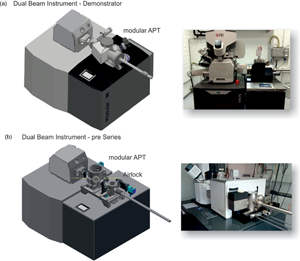
In the ongoing development, initially a proof-of-concept demonstrator was constructed followed by a pre-series prototype. In this evolutionary process, some improvements were already incorporated. Since the whole design is modular, an additional equipment for dedicated sample treatments can easily be incorporated, and the design is also open to adopt different detector or laser systems from a range of compatible technologies. The layout of the demonstrator and the pre-series model are shown in Figure 1.
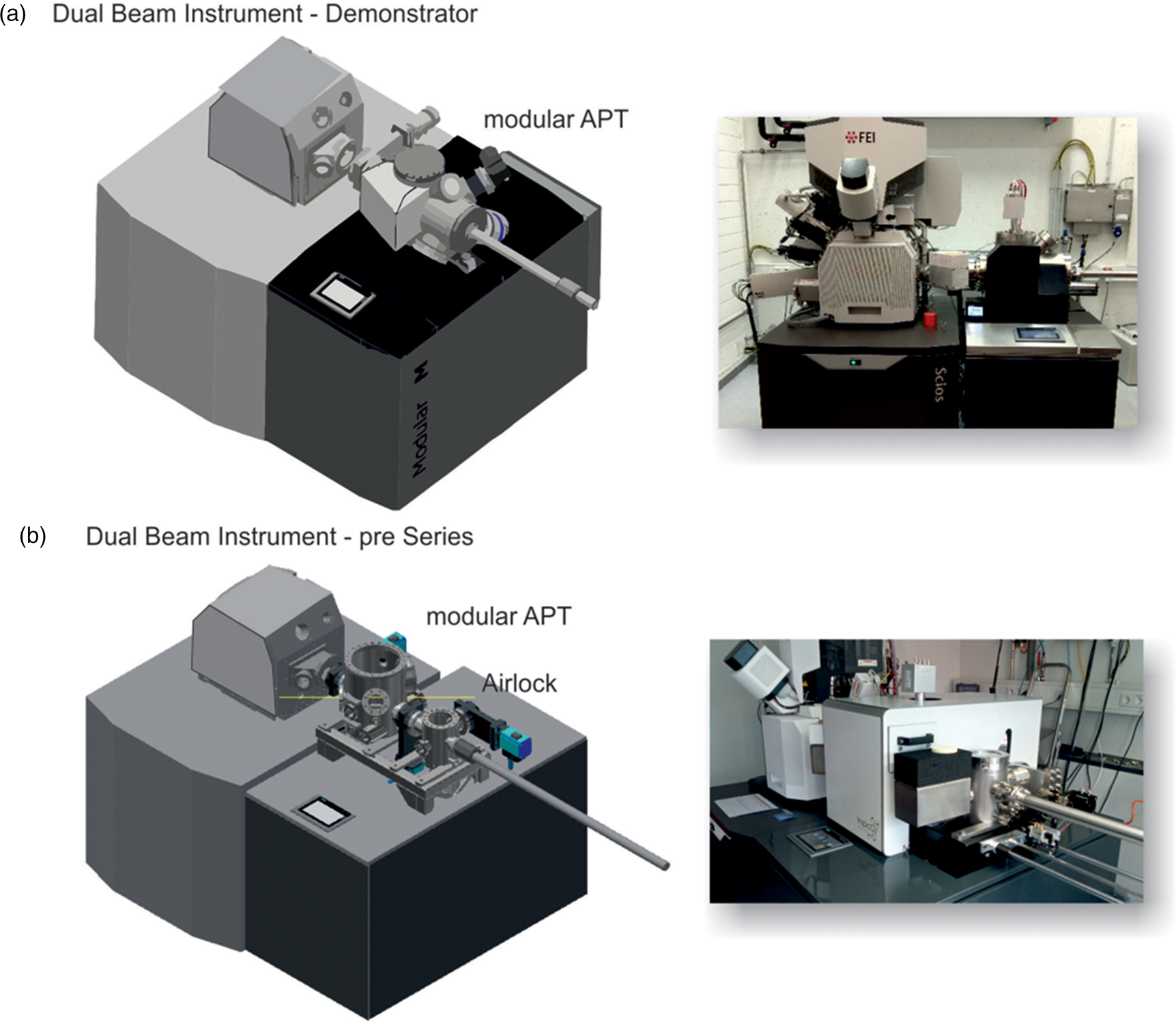
Fig. 1. (a) Demonstrator setup—combination of a dual-beam microscope and a modular atom probe connected via the load lock port of the SEM chamber (installed at the University of Stuttgart, Germany). (b) Second generation with an airlock chamber and a port to add a custom-designed experimental chamber (installed at the University of Ulm, Germany) (photographs with kind permission of INSPICO).
The APT Shuttle
In the simplest case, a magnetic transfer rod would be sufficient to move a sample holder between the two chambers if APT operation would follow conventional approaches. But we would like to make the instrument more flexible, so that the FIB can be also used for the maintenance and alignment of the microelectrode. The central piece of the Modular-Atom-Probe has been miniaturized and computerized by attaching modern micromanipulators to a moveable microscopic head of 4 × 6 cm2 footprint. This is the APT Shuttle (Shuttle) (Fig. 2).
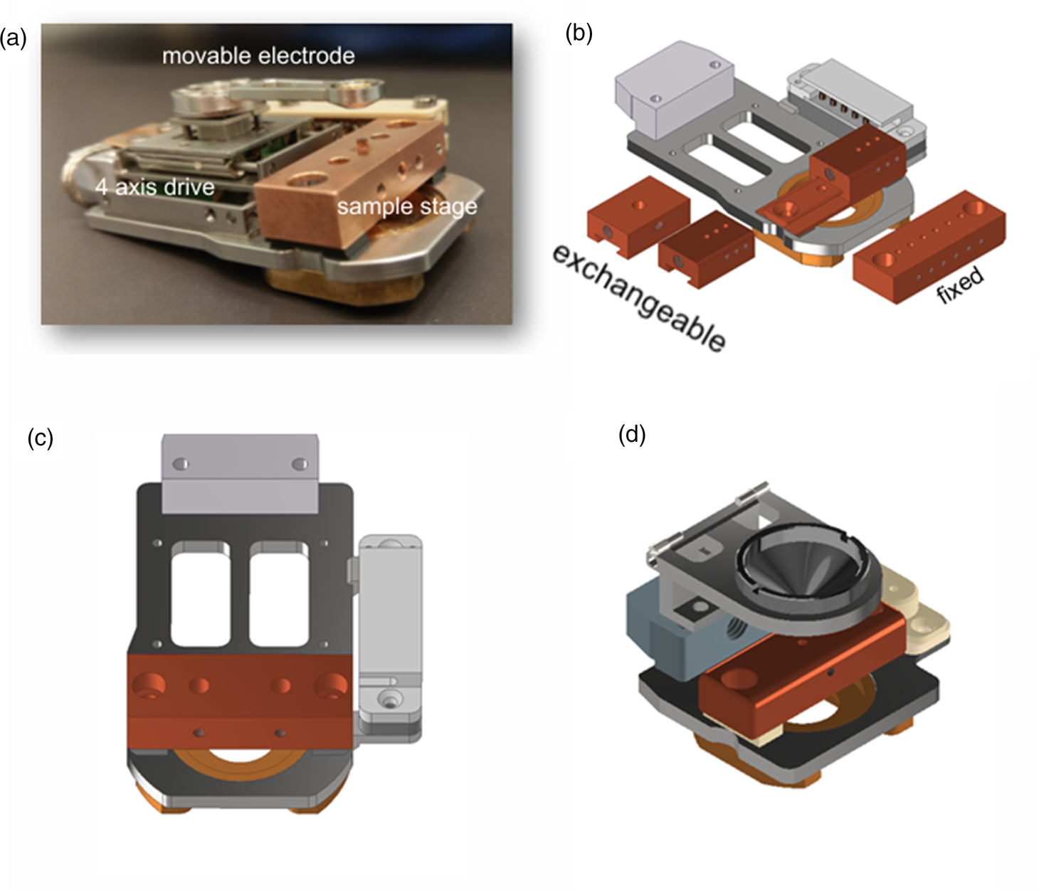
Fig. 2. (a) The transfer sample stage including the xyz and r movable extraction electrodes, (b) the sample stage can be modified and exchanged with regard to sample format (wires, TEM grids, cryo-samples, SEMstubs), (c) base plate providing electrical connectors and setup room for different experiments, and (d) a robust version with a mechanically adjusted macroscopic electrode version for student experiments.
This shuttle platform can be flexibly adopted to various experimental conditions as will be discussed later. The base plate provides an automatic electrical connector for high voltages up to 15 kV and additionally 10 more electrical contacts that can be used for multiple purposes. Currently, they are used to provide the necessary connection to the micromanipulators to position the extraction electrode in space by four independent axes. (X, Y, Z, and 360° rotation). The stages inside the FIB and APT provide matching counter pin plates that ensure mechanical contact when the shuttle is held in the position by a dovetail system.
The sample supports themselves are easily exchangeable (Fig. 2b–c), allowing adaptation to samples of various shapes. So far, single tips of metallic wire in copper, nickel, or stainless-steel tubes as well as SEM stubs and TEM half grids are standard. Via automatic contacts, all shown supports are connected to the cryo-lines in the APT and the SEM chamber as well. Two major categories of sample supports are offered: fixed versions and interchangeable ones. The fixed ones allow mounting the samples and exchange the extraction electrode outside the instrument on a mounting bench. The interchangeable ones are equipped with a miniature dovetail underneath and can be inserted via an extra transfer line. This can be a cryo-suitcase or via an extra manipulator, allowing transfer to parking positions or reaction chambers. Examples for the closed cryo-preparation routine will be described later.
In general, the shuttle can be modified in various aspects if custom solutions for unique experiments are needed. For example, a robust mechanical version for the analysis of metal samples is depicted in Figure 2d. The mechanically adjusted macroscopic electrode provides a simple to use version without the danger to brake sensitive piezo drives by unexperienced users.
However, the addition of the piezo-driven extraction electrode to the shuttle offers the following possibilities(Figure 3):
1. The high-resolution capabilities of the SEM can be used to inspect the quality of the extraction electrode prior to the measurement.
2. In the case of damage, the electrode can, in some cases, be machined by using the FIB beam for repair and to optimize measurement conditions.
3. The position of the extraction electrode can be adjusted using the high precision of the SEM. The tip position on the sample support is therefore flexible. Tips can be produced in situ (Halpin et al., Reference Halpin, Webster, Gardner, Moody, Bagot and MacLaren2019) at various positions and the electrode is adjusted accordingly.
4. The mechanical coupling of the tip and the electrode enables a faster switching between SEM and APT if intermediate SEM pictures of the tip are desired for calibration of the later reconstruction.
Fig. 3. (a) Prepared tip inspected by SEM, (b) adjusted extraction electrode above the sample viewed by an APT chamber camera, (c) adjusting the electrode inside the dual-beam instrument using the high resolution of the SEM, (d,e) preparation of a tip without lift-out at an arbitrary position, and (f) final electrode alignment (SEM view through the microelectrode).
Instrument Setup
The APT part consists of a single analysis chamber that is attached as a side chamber to the load-lock port of a commercial focused ion beam instrument. To combine both instruments, a custom-made load-lock adapter was developed bridging the gap between the Viton ring sealed vacuum system of the FIB and the UHV APT chamber. Since some of the commercially available cryo-transfer systems are also installed onto the load-lock port, the adapter has been designed to allow the addition of a Dewar for LN2 cooling (Fig. 1a) on the same port.
The APT measurement chamber uses an independent vacuum system. A pre-vacuum buffer is pumped by an oil-free scroll pump in cycling operation while no APT measurement is running and in continuous operation while the measurement mode is activated to create the necessary pre-vacuum for a turbo-molecular pump. The residual gas pressure in the measurement chamber is in the range of 2 × 10⁻⁹ to 8 × 10⁻¹⁰ mbar pressure, which is measured by ionization gauges. To decrease the vacuum level and to reduce hydrogen inside the chamber, the system is equipped with a 500 L/s non-evaporable getter pump. This pump must be activated depending on the number of transfer processes, usually once a month. The trapped hydrogen is evaporated by heating the NEG pump for a certain time. All chambers are made from stainless steel based on the conventional CF flange sealing technique and can be baked up to a temperature of 120 °C. The measurement chamber has a diameter of 200 mm and is designed for a vertical straight flight path. The horizontal axis allows transfer of the APT shuttle between APT and FIB. One laser entry and laser exit port are available. Two viewports CCD cameras allow monitoring the transfer and positioning of the samples inside the machine. Despite this, the necessary ports for the turbo-molecular-pump, non-evaporable-getter-pump, the magnetic transfer rod, and feedthroughs for high voltage and cooling are included.
The APT shuttle is held in the measuring chamber via a dovetail system on a piezo-driven hexapod stage with 6 degrees of freedom (X,Y,Z, rotation x, rotation y, and rotation z) that can be adjusted independently to position and orient the tip with regard to the laser beam. The sample stage operates in a closed-loop mode. The smallest adjustment travel is 1 nm lateral and 1 urad angular resolution. The repeatability of the sample position is ±200 nm laterally after a complete traverse of the stage, and the accuracy of the angular adjustment is ±10 urads. If the entire travel path is not used, the lateral repeatability is ±15 nm. Due to the high accuracy of the stage, sample positions can be approached very precisely. This allows the sample to be transferred back to the FIB to check the radius or other parameters. Afterwards, the measuring position is found again quickly by addressing the stored coordinates of the hexapod. The x and y coordinates for the sample to be measured can also be automatically approached from the SEM coordinates of the samples by means of a coordinate transformation. The position within the atom probe is overdetermined by the 6 degrees of freedom. Therefore, all rotations are initially left at 0 and can be readjusted by the user if necessary.
The electrical contacts are made via special UHV compatible pressure spring contacts. The necessary cooling is achieved via an electro-mechanical unit that presses an electrically insulated cooling plunger, which is connected to the cooling head via copper strips, against the APT shuttle (Fig. 4). Sufficient contact pressure is critical for the optimal cooling capacity of the actual tips. With the present design, a minimum temperature of <30 K is obtained.
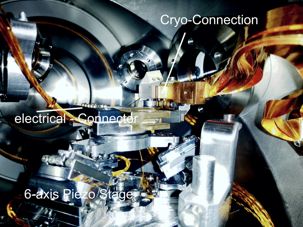
Fig. 4. Inside view of the measurement chamber (shuttle removed).
The initial design uses the FIB instrument as airlock and storage chamber, which reduces the complexity of the APT instrument. However, in a normal lab environment, the FIB is used for multiple purposes. A dedicated FIB, which is just used for APT, is seldom an affordable option. A normal atom probe measurement usually lasts several hours and in unique cases sometimes even several days. To avoid blocking the FIB from other service tasks during this time, an extra airlock chamber for the APT has been developed (Fig. 5b), which is attached in extension of the transfer axis.
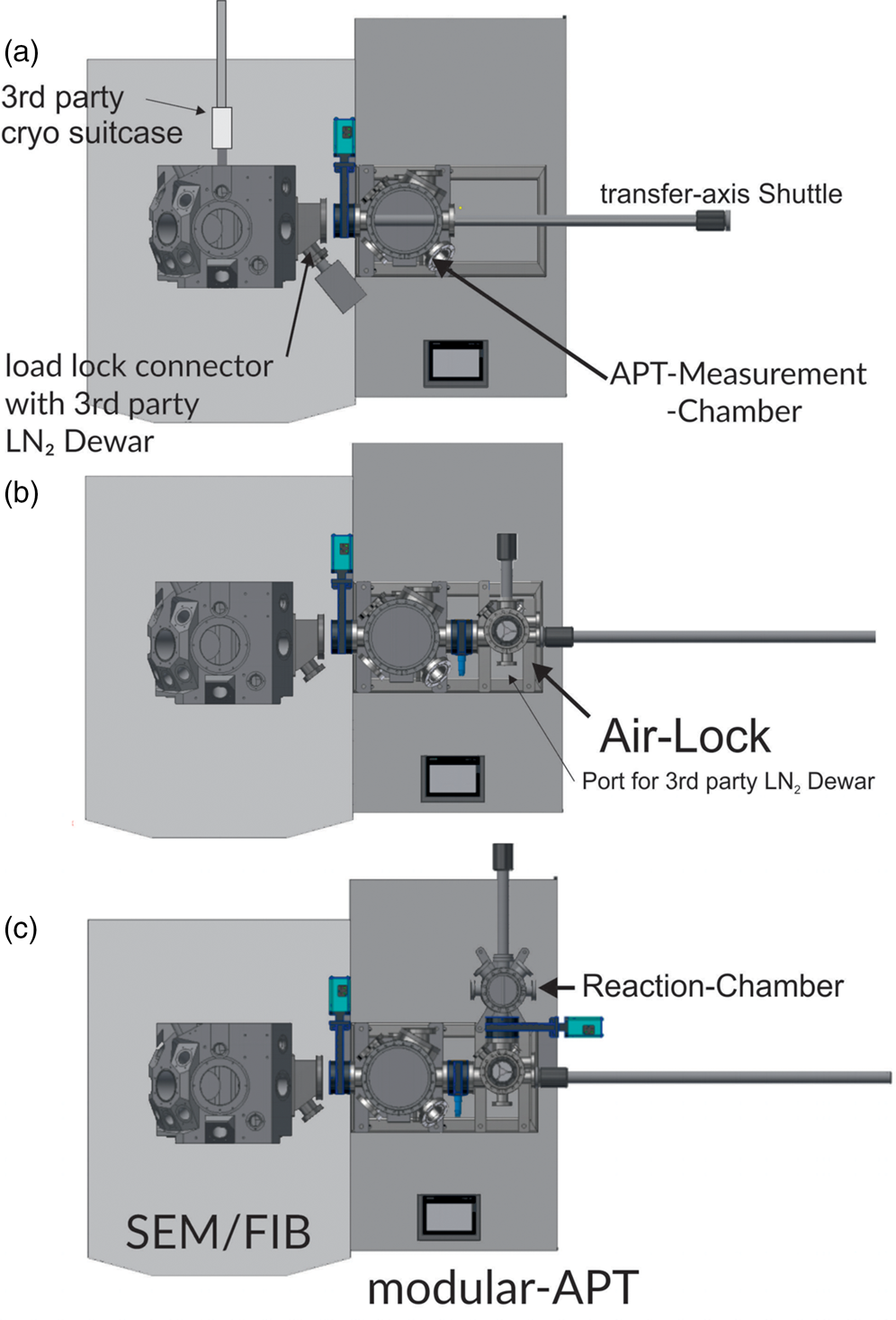
Fig. 5. Different instrument setups: (a) pure APT using FIB as airlock and preparation chamber, (b) the addition of a separate airlock chamber allowing independent loading of APT experiments, and (c) the addition of a further side experimental chamber.
The Airlock Chamber
The airlock chamber has been designed for two purposes. The first purpose is to allow a fast transfer of samples into the APT chamber without interrupting ongoing experiments in the focused ion beam instrument. Although not essential, it is convenient to have the option of inserting samples in multiple ways.
The chamber has been designed to hold multiple sample holders with a dovetail system on an internal stage. It thus also functions as a small storage unit. The special feature of the storage unit is that it can be connected to a Dewar via a flexible copper strip, which allows sample storage at about −140 °C. (Note that the “airlock” is operated as a pure storage unit when using this cooling option.) For the remote replacement of the exchangeable sample holders on the shuttle, an axis is required which is arranged at a 90° angle to the main transfer axis, which is also operated via a small magnetic transfer rod (see Fig. 5b).
The second purpose of the airlock chamber is to enable the addition of custom-made experimental chambers. Such experimental chamber can be located in the extension of the previously mentioned sample holder transfer axis (see Fig. 5c). Separated by a plate valve, an oven chamber, gas reaction, or liquid corrosion cell or similar may be attached to the available port. The transfer rod is extended accordingly. Thus, an undisturbed transfer between FIB, measuring chamber, lock chamber, and experiment chamber can be ensured without breaking the vacuum. Due to the existing cooled sample holders, this even allows an uninterrupted cold chain of the samples if the sample is also introduced cooled into the FIB by a suitable transfer unit. Of course, the airlock chamber could also be upgraded to provide a load-lock for a VCT500 (Leica VCT 500) or similar commercial suitcase for direct transfer of cooled samples. The airlock chamber is equipped with a turbo-molecular pump connected to the common pre-vacuum tank, reaching a base pressure of 10−8 mbar (Fig. 5b).
Cooling System
The samples located on the shuttle can be cooled to a minimum temperature of 30 K when located inside the measurement chamber. A two-stage Gifford-McMahon cryo-head is used to achieve this temperature. The temperature can be freely varied between 30 K and room temperature. The actual temperature is monitored by a Si-diode inside the vacuum chamber. The temperature is adjusted by changing the frequency of operation of the cryo-head and a nickel–chromium-resistant element acting as a heater directly on the cooling head surface.
Since vibrations are a critical issue for the stability of the laser and even more for the resolution of the SEM, extra measures have been undertaken to decouple and damp vibrations. The cryo-head is mechanically decoupled using a bellows. Transmitted vibrations are further damped using an elastomeric vibration damper in combination with oil pressure shock absorber. In addition, the entire chamber construction is mounted on air springs and decoupled from the FIB by another bellows and additional elastomeric dampers.
The design measures taken reduced the vibrations to an acceptable level but did not eliminate them completely. Thus, reductions in SEM resolution are unavoidable when the cryo-head is in operation. The resolution decreases to about 50 nm when the cryo-head is in operation. Similar negative effects are known for cryo-EM solutions available for biological samples. But still, both systems can be reasonably operated simultaneously.
Lift-out samples can still be made and tip-shaped samples can be prepared by azimuthal milling. The same applies to EDX analyses and lamella preparation for the transmission electron microscopes. Only for high-resolution images and the final thinning of lamellae, the cooling head and thus the measurement must be paused for a short time. The further reduction of vibration is a subject of current development.
Sample cooling inside the airlock chamber and the FIB (Fig. 6) is achieved via the use of LN2 dewars connected by copper stripes to the respective sample stages. A cryo-stage has been developed for the FIB enabling the exchange of samples using a Leica sample suitcase (Leica VCT 500) and keeping a base temperature of −145 °C. The suitcase has also been modified to accept the dovetail-based sample holder.
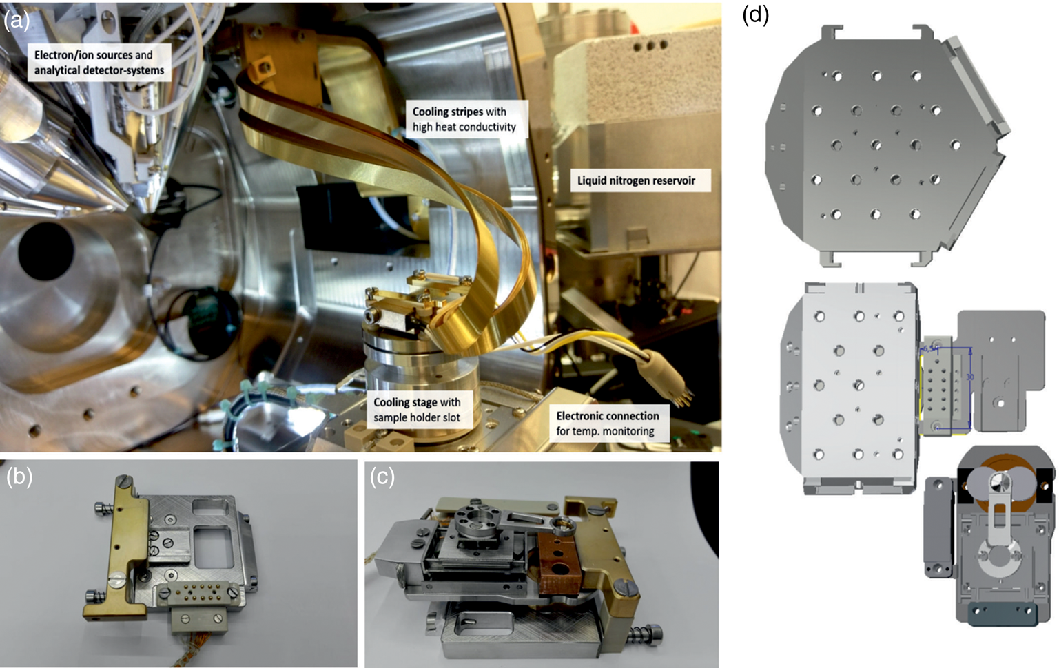
Fig. 6. (a) Leica cooling setup for the FIB, dedicated cryo-stage inside the FIB chamber without (b) and with (c) mountedAPT shuttle under cryo-conditions using the provided Leica cooling stripes and Dewar, and (d) (upper part) standard SCIOS sample stage for SEM stubs (lower part) modified sample stage to also accept the APT shuttle without cryo-option.
Hard–Software Interface
The control of the system, the measurement, and the subsequent reconstruction are performed by three independent computer systems, which in turn operate completely independently of the FIB/SEM systems. All basic functions of the atom probe are monitored and switched by a programmable logic controller (PLC). The unit monitors the vacuum conditions and takes over the control of the pumps and valves. Critical system conditions that could lead to damage to installed components are intercepted and incorrect operation is prevented wherever possible. The system operates independently of the connected FIB. Only through a hardware interface do both devices communicate during sample transfer. Compatible vacuum conditions are automatically checked before opening the separating plate valve to rule out unintentional flooding. The components required for the measurement are real-time controlled by a separate industrial PC. For this purpose, a control program was written that enables the control of the measurement parameters, data acquisition and display of the most important parameters on a monitor. Such parameters include laser energy, sample position, measurement rate, laser frequency, mass spectrum, visualization of events on the detector, multiplicity analysis, etc. TCP/IP protocol is mainly used for communication with connected components via Ethernet ports. For measurement/control of analog components a dataaAcquisition (DAQ) card is used. Data from the detector is acquired using a time-to-digital converter (TDC) card. This has a minimum resolution of 25 ps per bin. The data is continuously read out in a separate thread, analyzed and filtered based on the consistency parameters of the delay line detector. In packets of 25,000 events, they are streamed to a physical disk, stored in the open source, binary RAW file format. The data is later transferred to another computer for reconstruction. In the event of a program crash or other error condition of the system, the laser is stopped. The high voltage remains at the last set value. Sample cooling, vacuum system and other systems remain active as long as no critical system state is detected by the PLC. In case of a critical condition, all components are deactivated. In the event of a power failure, the system will remain in a standby state. All valves are closed without power. The measuring computer can read the state of the PLC but cannot influence it. The subsequent reconstruction is done on an independent work station. In principle, the reconstruction software runs on all computers with a dedicated graphics card. However, the available main memory influences the maximum number of displayable measured atoms.
Detector and HV System
The detector system for the prototype instrument consists of a resistance matched chevron stacked micro-channel plate (MCP) detector with a proven open area ratio (OAR) ratio of >70%, 12 μm pore size, and an active diameter of >75 mm. The MCP setup can be replaced by newly available funnel MCP with an OAR of 90% increasing ion detection efficiency above 80% (Fehre et al., Reference Fehre, Trojanowskaja, Gatzke, Kunitski, Trinter, Zeller, Schmidt, Stohner, Berger, Czasch, Jagutzki, Jahnke, Dörner and Schöffler2018). A 120 mm two-dimensional wire coil delay line is used for position readout, with a pitch distance of 1 mm. The single pitch propagation time for the two layers is determined to be 1.21 ± 0.05 and 1.24 ± 0.05 ns. Two signals with a distance of 1 mm between the output points would therefore have a time difference of about 2.5 ns. The delay time from one end of the delay line to the other end is necessarily a constant. It is about 150 ns. This constant can be used to identify pairs of signals that belong together even if several signals arrive within the same detection window (Multi-Hit Event). This time sum signal has a sharp distribution around the expected value with a (Full Width at Half Maximum) FWHM of 500 ps. Thus, theoretically, two signals could be separated from each other if they possessed a minimum separation of about half a millimeter. Delay line signals are amplified and processed by fast constant fraction discriminators with a maximum bandwidth of 300 MHz and a double hit dead time of 10 ns, which corresponds to an inactive relative impact position distance of 8 mm. For improved Multi-Hit detection capabilities, the 2D line can be replaced by an hexanode delay line. The Multi-Hit resolving power is just limited by the width of the time sum signal (Jagutzki et al., Reference Jagutzki, Cerezo, Czasch, Dörner, Hattaß, Huang, Mergel, Spillmann, Ullmann-Pfleger, Weber, Schmidt-Böcking and Smith2002). The system is also prepared to use a hexanode in view of high-voltage supplies, the chamber flange size, and the control and filter algorithms. Digitized timing events are measured by a TDC with 25 ps bin size resolution. For signals stemming from the MCP used as timing information for TOF spectroscopy, pulse intensity signals are recorded in addition. The double-pulse resolution accounts to <5 ns, while an unlimited number of Multi-Hit events can be recorded (Cronologic).
Contrary to the design of earlier systems (Stender et al., Reference Stender, Oberdorfer, Artmeier, Pelka, Spaleck and Schmitz2007; Schlesiger et al., Reference Schlesiger, Oberdorfer, Würz, Greiwe, Stender, Artmeier, Pelka, Spaleck and Schmitz2010), the high-voltage system is not directly controlled by the measuring computer. A separate microprocessor with 24-bit DA-AA converters takes control of the high voltages. A voltage between 0 and 10 V is output to control the power supplies. The information of the voltages to be set and the measured control voltages are exchanged asynchronously with the measuring computer via an Ethernet connection using the TCP/IP protocol.
Precise voltage sources with a ripple V pp of <7 mV are used for the detector system. According to the aperture listed in Stender et al. (Reference Stender, Oberdorfer, Artmeier, Pelka, Spaleck and Schmitz2007), a voltage of −3 to +3 kV can be variably applied to the input aperture in front of the detector. Depending on the applied voltage, this leads to an enlargement/reduction of the field of view. It can be raised proportionally to the applied base voltage. Since this cancels the independence of the point of impact on the detector from the ion mass, the value is recorded for each event. By default, however, the aperture is at ground potential and is currently only used for test purposes.
The base voltage can be varied from 0 to 12 kV. The ripple factor is 10−5. With these values, the resulting error of the power supply would account to 2.4 V at 12,000 kV and thus limit the mass resolution, according to simple Gaussian error propagation theorem, to m/Δm of 1/5,000. The 24-bit converter allows the voltage to be varied in minimum units of theoretically 0.7 mV, which is much better than the expected error level of the power supply itself.
Laser System
The laser pulses required for controlled evaporation are generated by an industrial laser system. The reliable laser sources are mounted below the chamber as a single unit, which is damped on air springs. While the demonstrator is equipped with a 10 ps pulse width laser, the second generation is equipped with a 350 fs laser system. Both systems use infrared as the fundamental wavelength (1,034 nm) and provide both the second harmonic 517 nm and the third harmonic 344 nm. Switching between the wavelengths is possible by manually exchanging the polarizer unit. Usually, however, the third harmonic oscillation is used for the experiments. The sample is moved into the focused laser spot in the chamber via UV-sensitive camera optics arranged similar to a confocal microscope. The final lens is located inside the vacuum chamber with a short focal length of 40 mm. The spot size achieved is currently <8 μm in dependence of the chosen beam expansion factor. The laser spot can be scanned in a limited area via a high-frequency piezo tilting mirror system. The scanning system has a resolution of 0.2 μrad and a repeatability of 0.4 μrad and operates in a close-loop mode with a response time in the ms range (Fig. 7).
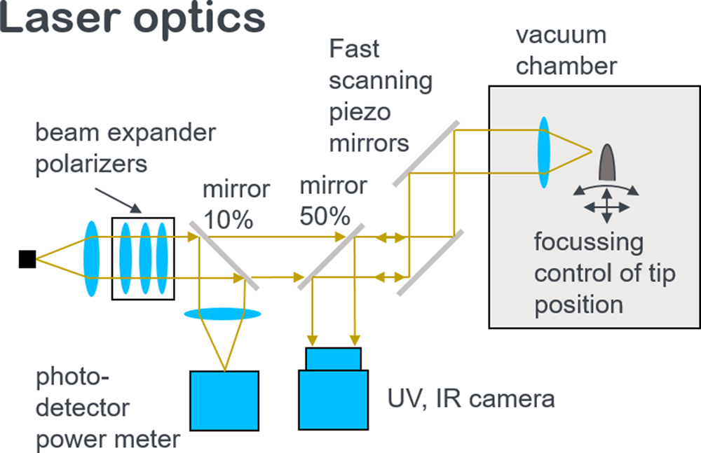
Fig. 7. Laser system.
In order to cover a wide range of measurement conditions, the laser system can be adjusted using various parameters. The polarization direction of the incident laser light can be rotated 360° and thus freely selected. By default, a polarization direction parallel to the sample axis is selected. The pulse energy can be varied between the maximum pulse energy of 10 μJ and practically zero in 2,048 steps. The repetition rate, in turn, can be varied between single shot and the maximum frequency of the laser system used. The range of values for the picosecond system is 1–1,000 kHz, while for the femtosecond system it is between 1 and 2,000 kHz. The spot size can be changed to a small extent by a manually adjustable beam expander, while it cannot be selected larger than 10 μm. To measure the actual laser energy, a small part of the laser light is coupled out via a beam sampler and continuously measured with a Si diode.
The focal plane within the vacuum chamber is determined by the focal length of the final lens. The position of the tip relative to the focal point be changed using the piezo stage, and controlled by a camera, which captures the light backscattered from the chamber via a beam splitter. The setup is based on the setup of confocal microscopy. If the tip is at the focal point, the image in the camera will have maximum sharpness.
Characteristics
With a flight length of 105 mm, the geometrical opening angle accounts to ±20°. Due to image compression arising from the tip geometry, the observable opening angle is larger, as can be derived from the pole figure observable from a tungsten measurement depicted in Figure 8. The poles (011) and (112) are resolved. Using them for calibration, the image compression factor κ is determined to be 0.54 in accordance to earlier determined values (Stender et al., Reference Stender, Oberdorfer, Artmeier, Pelka, Spaleck and Schmitz2007), which fixes the effective aperture angle to ±37° for the sample presented in Figure 8.
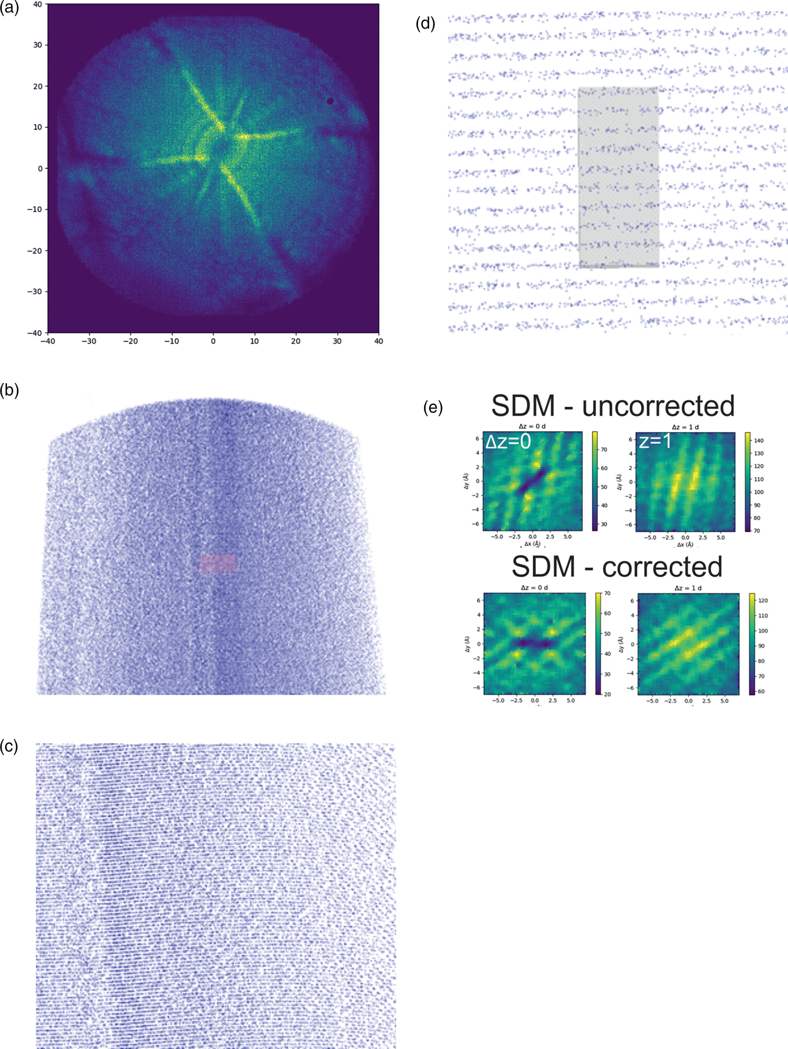
Fig. 8. (a) Desorption map of tungsten, (b) reconstruction of a tungsten measurement revealing lattice planes, (c) magnified view demonstrating two sets of lattice planes, (d) lattice planes zoomed-in (inset dimension 1 nm × 2 nm), (e) spatial distribution maps calculated in the x–y plane, and (f) calculated lattice spacing along the z-axis.
The mass resolution was tested by measurements on tungsten, aluminum and nickel samples, among others. The mass resolution m/Δm, determined over the full width of the detector, is for the aluminum measurements with a FWHM of (0.039 ± 0.001) u at m = 27 u about 700 (692 ± 20). Somewhat lower values were found for nickel with m/Δm = 612 ± 12 and tungsten with m/Δm = 683 ± 10. The signal-to-noise behavior spans a dynamic range of up to 3.5 orders of magnitude (Fig. 9).
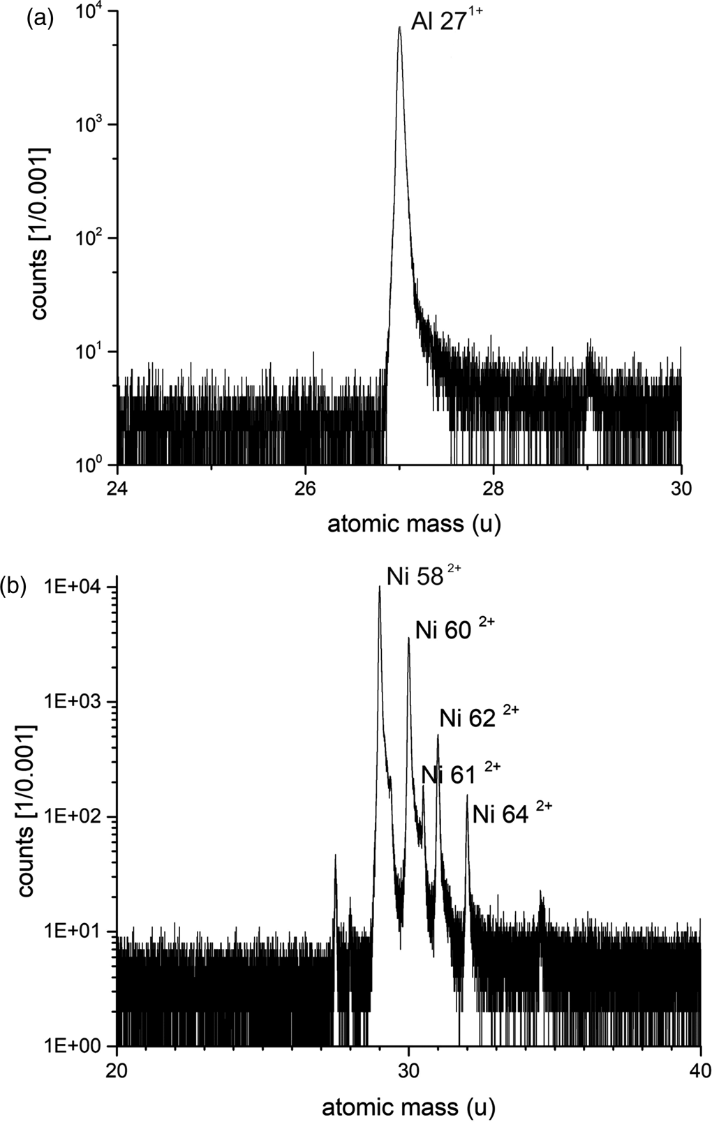
Fig. 9. Mass spectra of an exemplary aluminium (a) and a nickel sample (b).
The OAR of the used microchannel plate is specified to be 70%. In order to determine the detection efficiency, the reconstructed volume must correctly match the lattice properties of the real physical sample. While the z-resolution is typically sufficiently high to resolve the individual lattice planes and, thus, the required z-scaling, the correct scaling of the lateral directions is less obvious. It was shown by Geiser et al.'s maps (Geiser et al., Reference Geiser, Kelly, Larson, Schneir and Roberts2007) that spatial information in the lateral directions can still be obtained from atom probe data using the so-called spatial distribution maps (SDMs).
An SDM is a two-dimensional histogram visualization of all interatomic distance vectors:
 $${\rm \Delta }\overrightarrow {r_{ij}} = ( {{\rm \Delta }x_{ij}{\rm \Delta }y_{ij}{\rm \Delta }z_{ij}} ) $$
where the lateral components, i.e. Δx ij and Δy ij, are chosen here for the two-dimensional histogram data. Depending on the lattice type and orientation, preferred combinations Δx ij, Δy ij exist which will be seen as maxima in the histogram.
Geiser et al. (Reference Geiser, Kelly, Larson, Schneir and Roberts2007) showed that the lateral resolution is optimized if the Δx ij, Δy ij are chosen for atomic pairs within a very narrow Δz-separation. In a first step, the sample volume is optimally aligned in the z-direction using statistical criteria, from which the z-scaling factor for the correct lattice spacing is also obtained. Then, all pairs Δx ij, Δy ij are chosen for which
 $${\rm \Delta }z_{ij} < 0.1\;\;{\unicode{x212B}}$$
holds. The resulting histogram is shown in Figure 8e (upper part) after the application of a Wiener filter for data smoothing.
As can be seen, lateral information does exist in this histogram; however, the lattice is obviously distorted. Since the real crystallographic positions of these maxima are known, the histogram can be transformed by taking two linearly independent maxima (determined by two-dimensional Gaussian fits) and solving a system of linear equations to obtain the transformation matrix. The result is shown in Figure 8e (lower part). With knowledge of the real volume corrected this way, the detection efficiency is obtained as 68 ± 8%. (Note that lateral information is also visible for atomic pairs that do not stem from the same lattice plane Δz = 0, but also for pairs from neighbouring planes with
 $${\rm \Delta }z = d_z$$
where dz is the lattice spacing in the z-direction. The determined detection efficiency agrees with the value expected from the OAR of the MCP within the limits of error accuracy. Similar results have been reported earlier (Fehre et al., Reference Fehre, Trojanowskaja, Gatzke, Kunitski, Trinter, Zeller, Schmidt, Stohner, Berger, Czasch, Jagutzki, Jahnke, Dörner and Schöffler2018).
Experimental
The samples are prepared, and the microelectrode is aligned in the FIB before measurement. The shuttle is then transferred to the atom probe chamber. An experienced operator needs about 30 s for the complete mechanical transfer. However, the different vacuum levels prove to be critical here. Ordinary FIB instruments work in a pressure range of 10−4–10−6 mbar. An improvement of the vacuum into the high 10−7 mbar range is observed when operated in cryo-experiments. The typical working pressure in the atom probe is between 10−9 and 10−10 mbar. For the transfer of the shuttle, the intermediate plate valve must be opened, so that there is an inevitable deterioration of the vacuum level in the APT due to the transfer process. A regeneration time of about 30 min is observed to return to the medium 10−9 mbar. However, the risk of thawing for temperature-sensitive samples is avoided by the permanent cooling inside the APT. Even if the actual transfer takes only a few seconds, an immediate start of high-quality measurements after the transfer has to be avoided due to the vacuum restrictions.
On the good side, the instrument offers new opportunities for a quick sample check if the mass spectrum suddenly shows a deterioration during the measurement. As an illustrative example, Figure 10a shows an aluminum tip before the measurement. In the SEM picture, the typical vibration artifacts are seen that are caused by the cooling head. The sample was analyzed for about 10 million measured atoms (see reconstruction in the inset of Fig. 10a) when the signal-to-noise ratio collapsed drastically. A flashover or a break-off of the sample was expected. To check, the sample was transferred back to the FIB for inspection (Fig. 10b) showing directly the damage of the sample probably caused by an electrical sparkover between the sample and the extraction electrode. Since there was still enough material left, the sample was then directly sharpened again and the measurement was continued after about 30 min total processing time (see Fig. 10c) to count another 107 atoms. For even faster transfer and measurement, a dedicated UHV FIB would be a viable option.
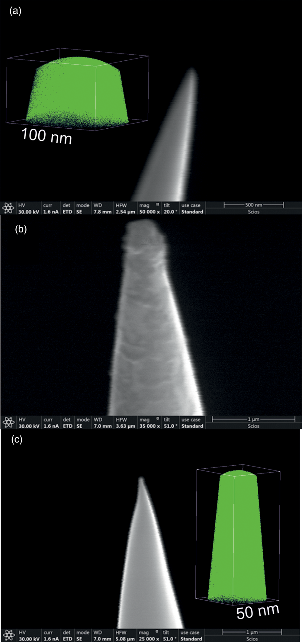
Fig. 10. (a) Aluminum sample before measurement, (b) after flashing event, and (c) after reshaping.
Air-Sensitive Samples
Due to the direct exchange between preparation and measurement, the instrument is especially suited for the analysis of samples sensitive to air or moisture. As an example of such a sensitive sample, a pure lithium tip was prepared by lift-out, since this metal plays a predominant role in battery science and immediately reactions with nitrogen or moisture. The material was previously stored in a glovebox under argon protective atmosphere. Using a transfer system (Leica VCT 500), it was transferred to the FIB/SEM under an inert gas. After preparation, the sample was transferred directly into the attached APT chamber and the measurement was started.
The corresponding mass spectrum is shown in Figure 11. As expected, mainly lithium is detected. Small traces of gallium, despite careful cleaning steps at 2 kV accelerating voltage, and H2O and OH3 are detectable at the surface. Regarding the water, the exact origin is unclear. It may be ionized molecules from the residual gas of the measurement chamber, or actual adsorbed impurities formed in the poorer vacuum of the FIB. Even, if this example of a pure metal has no significance from a materials science point of view, it shows the possibility of protecting a sensitive sample from unwanted reactions or even destruction and inserting it to the atom probe measurement. While the sample here was transferred to the FIB with the aid of a transport device, the sensitive material could also be protected by a cover layer that is milled away by the FIB. Then, no additional transfer system would have been necessary.
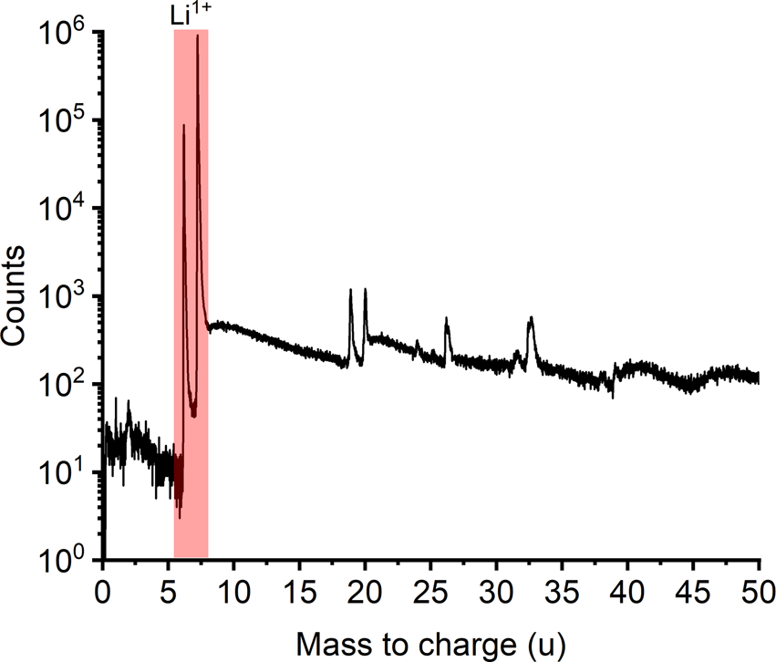
Fig. 11. Mass spectra of an exemplary lithium measured at 30 K, 200 kHz repetition rate, wave length 355 nm, and pulse energy 1 nJ.
Cryo-Samples
The preparation and measurement of cryogenic samples for cryo-APT is a very laborious and error-prone process. The modular version was specifically designed to simplify at least part of the process and eliminate unnecessary sources of error. Thus, the group has succeeded in performing fundamental analyses on frozen liquids (Schwarz et al., Reference Schwarz, Dietrich, Ott, Weikum, Lawitzki, Solodenko, Hadjixenophontos, Gault, Kästner, Schmitz and Stender2020, Reference Schwarz, Dietrich, Ott, Weikum, Lawitzki, Solodenko, Hadjixenophontos, Gault, Kästner, Schmitz and Stender2021). The preparation of these samples with intermediate transport in a shuttle solution is also possible. However, it requires at least two more lock and transfer processes. Normally even three. With each process, there is a risk of losing the sensitive sample. The production time per tip, using a conventional Ga FIB, accounts to 3–5 h per tip. This complex manufacturing process limits the sample throughput and makes any loss even more significant. In the first measurements, to avoid unwanted interference, all uninvolved areas were previously cleaned of frozen sample components. Therefore, unwanted side reactions in the fundamental data could be excluded. An example mass spectrum of a frozen liquid, in this case honey, is presented in Figure 12. Now that the fundamental information are collected for various systems, new protocols can be developed with the goal of increasing sample throughput.
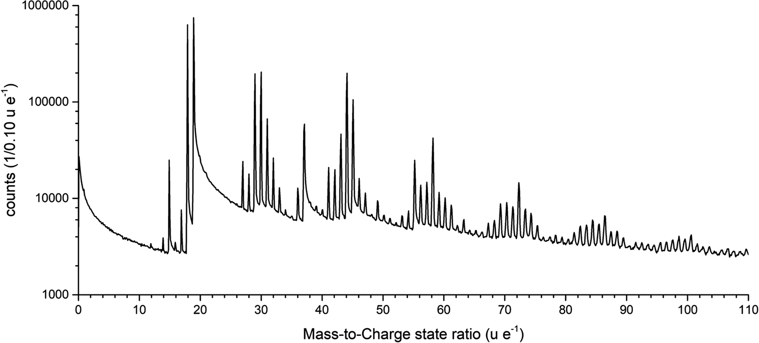
Fig. 12. Mass spectrum of a honey with a mass-to-charge state ratio from 0 to 110 u e-1 as a logarithmic plot.
The goal now is to take advantage of the fast sample transfer and to minimize processing times and maximize the measured volume. One opportunity will be, to prepare only the topmost part of the droplet and feed it to the measuring process. This will allow the cutting process to be restarted after the measurement has been completed and thus a larger area to be measured from the same sample. It would reduce the initial milling time while allowing access to larger sample areas compared to the previous experiments and represent the unification of all previously presented capabilities.
Reconstruction Software
For the reconstruction of the data, an independent software solution based on OpenGl and C++ was developed (Reference Stender and BallaStender & Balla, n.d.). The raw data are stored in a binary data format that was also used by the previous instruments (Stender et al., Reference Stender, Oberdorfer, Artmeier, Pelka, Spaleck and Schmitz2007 ; Schlesiger et al., Reference Schlesiger, Oberdorfer, Würz, Greiwe, Stender, Artmeier, Pelka, Spaleck and Schmitz2010). Other file formats such as “pos” and “epos” are supported (Reference Gault, Moody, Cairney and RingerGault et al., n.d.). However, only the raw format allows the full use of all functions so far. The software is being continuously developed to be open to other data formats as proposed by the IFES (International Field Emission Society) technical committee. The software offers simple filtering options of the raw data, mass spectra with bowl correction, and a graphical alloy editor with the SQL database for already defined molecules. The tips can be reconstructed with different reconstruction modules following the protocols of Bas et al. (Reference Bas, Bostel, Deconihout and Blavette1995) and Jeske & Schmitz (Reference Jeske and Schmitz2001). For the geometric reconstruction algorithms, there is an additional possibility to use parameterized curves for the shaft angle of the tip. For the filters as well as for the reconstruction parts of the software, there is the possibility to insert own modules in Java-Script and to manipulate the data accordingly. Various export formats allow the data to be transferred to other software solutions. After successful reconstruction, the peak is displayed as a color-coded point cloud as usual. The representation of the data can be adjusted by manipulating the data stream using element and geometry filters. Data evaluation currently includes isosurfaces and orthoslices, composition profiles, cluster search algorithms (Lawitzki et al., Reference Lawitzki, Stender and Schmitz2021), nearest-neighbor analyses, and SDMs (Geiser et al., Reference Geiser, Kelly, Larson, Schneir and Roberts2007). The aim is to further expand the number of possible evaluation modules.
Summary
In established atom probe analysis, the APT for controlled field desorption and the FIB microscope for sample preparation are operated as two separated instruments. To enable fast cryo-transfer and to introduce new operational modes in the maintenance and alignment of extraction electrodes and tip, we presented a new instrument that represents basically a direct combination of APT and a dual-beam scanning microscope. The necessary internal and mechanics to realize a fast cryogenic sample transfer has been developed and demonstrated. Sensitive samples can be prepared and transferred to the APT without breaking the vacuum and without an additional transport device within a few seconds. The same applies to frozen liquids or samples that need to be permanently cooled and protected from atmospheric influences.
Due to the fast transfer between the units, samples can be easily re-tipped and further measured. SEM images before and after the measurement can conveniently provide information about the actual evaporated volume. The extraction electrode, which is often affected by dirt or electrical flashovers, can be inspected easily in the scanning electron microscope and, if necessary, reworked by the ion beam.
The atom probe performance data in terms of mass resolution, aperture angle, detection efficiency, and signal-to-noise ratio demonstrate a reliable analysis without compromises in comparison to dedicated stand-alone instruments.
Remaining mechanical vibrations transferred from the cryo-stage to the FIB and long vacuum restoring time after transfer are presently the main limitations, but could be certainly further improved by raising the vacuum quality in the FIB and decoupling the cryo-head via a gas reservoir.
The aspect of modularity does not only refer to the possibility to connect the APT as Ad-On to a FIB/SEM or any other device. It also includes the interchangeability of the measuring head (APT shuttle) and/or the adaptation of this to special measuring conditions. The exchange of the measuring heads is as uncomplicated as the sample exchange. In addition, experimental chambers can be attached to the airlock chamber. The airlock chamber can be used for simple sample introduction, sample storage (cooled and uncooled), or as an exchange chamber. Also, the positions of the chambers can be rearranged, within the geometric limits of the rack if special circumstances require it. However, equipped with an airlock chamber, the instrument can also be used separately from all other instruments in the usual way for the analysis of APT samples.
Funding
This work was supported by Bundesministerium für Bildung und Forschung. (VIP 03V0756).


 Open access