


Crossref Citations
This article has been cited by the following publications. This list is generated based on data provided by Crossref.
SAKUDA, Yusuke
ASAHINA, Shunsuke
TSUTSUMI, Kenichi
and
ONODERA, Hiroshi
2020.
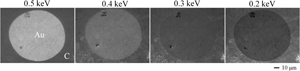
Study of Reversal Contrast Phenomenon in SEM Images at Low Incident Accelerating Voltage by AES.
Vacuum and Surface Science,
Vol. 63,
Issue. 6,
p.
294.