


Introduction
The interest in performing in situ transmission electron microscopy (TEM) experiments is continuously growing. Such experiments can, for example, involve exposing a material to mechanical deformations (Morrow et al., Reference Morrow, Cerreta, McCabe and Tomé2015), external heat (Kumar et al., Reference Kumar, Konrad, Chakravadhanula, Dehm, Wang, Wenzel, Krupke and Kübel2019), or bias (Kamaladasa et al., Reference Kamaladasa, Sharma, Lai, Chen, Salvador, Bain, Skowronski and Picard2014). Additionally, in situ experiments can be conducted in gaseous (Straubinger et al., Reference Straubinger, Widemann, Belz, Nattermann, Beyer and Volz2018) or liquid (Su et al., Reference Su, Wang and Wang2019) environments to study various reactions. Combinations of these external stimuli are on some occasions possible as well. One challenge to perform such experiments is the fabrication of suitable samples for the analyses. In this work, we present our focused ion beam (FIB) technique to create TEM lamellas for in situ thermal and electrical measurements. These measurements require the sample to be attached to a chip that is based on microelectromechanical systems (MEMS). Such a chip is controllable via software and can, for instance, be heated to bring the specimen to a certain temperature. Our demands on the sample are diverse. It should be possible to thin both sides of a sample to electron transparency on the chip. The electron transparent area should be suitable for high-resolution TEM and feature a low amount of preparation-induced artifacts and contamination. Furthermore, the technique should be flexible and mainly require a FIB machine equipped with a micromanipulator. The only necessary extras are a few simple, custom-made FIB holders, which can be easily created by any workshop. The specimen should have good contact to the chip and be mechanically stable. Lastly, the procedure should be applicable to a wide range of materials. There exist some procedures on how to create similar samples, but we wish to expand the range of possible approaches (Duchamp et al., Reference Duchamp, Xu and Dunin-Borkowski2014; Vijayan et al., Reference Vijayan, Jinschek, Kujawa, Greiser and Aindow2017; Tunes et al., Reference Tunes, Quick, Stemper, Coradini, Grasserbauer, Dumitraschkewitz, Kremmer and Pogatscher2021).
Materials and Methods
The FIB sample preparation is demonstrated on a layered silicon structure. An initially crystalline silicon layer, which was grown on the top of a silicon on insulator wafer by molecular beam epitaxy, is amorphized by silicon ion implantation at the Helmholtz-Zentrum Dresden-Rossendorf. More information about this material can be found in Radić et al. (Reference Radić, Hilke, Peterlechner, Posselt, Wilde and Bracht2020). For the demonstration of the sample's quality we use a single-crystalline NiAl specimen.
The MEMS chips utilized in this work are Protochips Fusion Select chips. These are available in various configurations, ours are purely intended for heating experiments but further options for electrical characterization exist and the procedure is generally applicable to those as well. The chips consist of a silicon carbide membrane and are in our case coated with an amorphous holey-carbon film. The carbon film seems to yield a better adhesion of the sample to the chip, but other than that, it is not necessary for our materials or application.
The FIB machine used for the fabrication process is a ZEISS CrossBeam 340. The liquid metal ion source of this device is gallium. A platinum precursor gas is used for all deposition steps. The machine is equipped with an MM3A-EM micromanipulator by Kleindiek without a rotation option for the manipulator needle.
TEM analyses of the samples are performed on a ThermoFischer Scientific (FEI) Titan Themis G3 300 microscope. It features an image Cs corrector along with a Gatan Quantum 965 ER. The high tension is set to 300 kV for the analyses.
For our approach and demands on the sample, we envisioned a design as shown in Figure 1a. The area of interest is placed on the top of a hole in the chip, and large pads on the sides provide good contact and stability. The sample is not just a flat lamella but has a slightly more complex shape. Its area of interest protrudes above the hole and is nearly parallel to the chip's surface in order to be able to thin both sides of the structure.

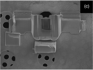
Fig. 1. A schematic render of the envisioned structure on a chip (a) and a SEM image explaining terms used throughout the text (b). The “FIB stub” is shown in (c) along with the indication for “block A.” The “cube stub” can be seen in (d), while (e) portrays how this stub is utilized to flip the “FIB stub” by 90°. It is crucial that “block A” is the upper piece after the flip. The pre-tilted chip holder can be seen in (f). The pre-tilt amounts to 36°. A thin metallic clamp gently presses onto the chip to keep it in place.
Before explaining the sample preparation in detail, we want to clarify some terminologies and present the custom holders needed for the procedure. Our definitions of some terms regarding the specimen structure are shown in Figure 1b. These terms will be referenced throughout the sample preparation guide.
In total, three custom SEM stubs are necessary for the procedure. The first of these holders will be called “FIB stub” and is simply used to hold a FIB grid. Its design can be seen in Figure 1c. The “FIB stub” features, as usual for such holders, a small ledge to easily position the FIB grid between the clamps. This stub is special in the sense that the two clamping blocks are rather narrow. Especially one of these pieces must be thin with a thickness of  $\approx$1 mm, we call this piece “block A.” The reason behind this restriction is that the entire “FIB stub” containing the FIB grid will be flipped by $90^{\circ }$ during the process. A thin “block A” is necessary to prevent the micromanipulator from touching the stub after this flip. The FIB grid must be inserted into the “FIB stub” such that the flat sides of the posts are facing away from “block A.” In other words, the sample's front side has to face toward “block A” when it is mounted to the FIB grid.
The second stub has a cubic shape with a cylindrical hole and a screw perpendicular to this hole (Fig. 1d). The diameter of the hole matches the pin diameter of the “FIB stub.” This piece will be called “cube stub” and helps to flip the FIB grid by  $90^{\circ }$ as seen in Figure 1e. This step is necessary for the specimen fabrication in order to transfer the sample from the grid to the chip. Note how the flipped “FIB stub” and the “cube stub” form one plane surface. This reduces the risk of accidentally damaging parts of the machine during stage movements.
The last stub is the holder for the Protochip. It is pre-tilted by  $36^{\circ }$ and displayed in Figure 1f. At this pre-tilt and a stage tilt of $0^{\circ }$, the chip will be parallel to the ion beam. The Protochip protrudes from the holder such that it can be easily accessed by the micromanipulator. Additionally, an optimal gas flow from the gas injection system (GIS) is ensured. The chip is held in the stub by a thin metallic clamp.
Results and Discussion
Each material and each FIB machine are different. Consequently, we cannot give an universal recipe in terms of FIB energies and currents that will work for every case. Users are advised to determine these by themselves for the problem at hand. We will give our values for a rough orientation. The procedure on how to realize the desired sample is the following:
1. Bring the sample to the coincidence point, which is the point where the ion beam and electron beam are simultaneously in focus. Deposit a protective Pt layer (12 $\mu$m wide, 6 $\mu$m thick, 1.5 $\mu$m high) at the region of interest. This Pt deposition should initially be performed by electron beam deposition in order to induce less damage to the surface. Once a thin Pt layer has been created by the electron beam, the process can be stopped and continued by ion beam deposition using a 30 kv 300 pA ion beam. Afterward, mill two trenches to create a standard TEM lamella shape. However, this lamella is larger than usual with a width of 50 $\mu$m and a final thickness of about 4.7 $\mu$m. The depth of the trench should be around 10 $\mu$m. Position the two trenches such that the previously deposited Pt layer is centered. The trench milling is performed in two steps at an ion beam energy of 30 kV: at first, a beam with a current of 15 nA rapidly creates two large trenches at a tilt angle of $54^{\circ }$. The lamella is further thinned and cleaned in the next step with a beam current of 3 nA at an over-/undertilt of $2.2^{\circ }$. The resultant structure is shown in Figures 2a and 2b. All these images only serve to schematically illustrate the fabrication process, without scale bars.
2. In the next step, the stage remains tilted at
$54^{\circ }$, and 10 $\mu$m deep trapezoids are milled into the lamella with a 30 kv 3 nA ion beam. These trapezoids create the desired shape for the sample and in total three of them are necessary: one trapezoid at the Pt covered central area and two at the sides. The central trapezoid is 7 $\mu$m wide at its short side and $\approx$10.5 $\mu$m wide on the longer side. Its height is adjusted such that the lamella remains about 1.6 $\mu$m thick at the center. The trapezoids at the sides have the same height but are significantly wider. It is important to mill these trapezoids with the correct orientation. The trapezoid at the central area must face downward (meaning that its wider side is facing toward the backside), while the ones on the side are rotated by $180^{\circ }$. Instead of creating trapezoids, milling simple rectangles is possible too. Afterward, the stage is tilted to $0^{\circ }$, and the structure is cut free from the bulk on its left and bottom side using the same beam as before. Figures 2c and 2d display the material after these steps along with indicated dimensions.3. This step follows the usual technique for TEM lamella preparation by FIB: the stage remains at
$0^{\circ }$, the micromanipulator is inserted and mounted to the lamella with Pt by using a 30 kv 50 pA ion beam. The lamella is then completely cut free from the bulk with the 30 kv 3 nA beam. The lift-out procedure is performed by lowering the stage, and next the lamella is welded to a FIB grid on the “FIB stub.” We advise to use a larger and thicker Pt pad for this attachment, since the structure is heavier than a normal lamella. As previously mentioned, care has to be taken how the FIB grid is orientated in the “FIB stub.” Cut the micromanipulator free from the sample and fully retract it. The result after this step is displayed in Figure 3a.4. Next, readjust the eucentric height for the specimen and bring it back into the coincidence point. Tilt the stage to
$53^{\circ }$ and mill away the part with the diagonal cut on the left-side pad where the micromanipulator was previously cut free. Afterward, simultaneously polish the back side of both side pads by using one wide rectangular object spanning the entire sample. However, do not mill into the Pt layer keeping the sample connected to the FIB grid. The 30 kv 3 nA ion beam is used for these steps. The goal is to create a flat and clean surface at the backside, which is required to properly attach the structure to the chip. If the front side of the two pads is heavily contaminated with redeposited material, one can clean these as well. Care must be taken to keep the side pads at least $\approx$0.9 $\mu$m thick in order for the structure to remain stable. After the side pads are finished, the central area where the region of interest is located will be pre-thinned. This pre-thinned area should have a width of $\approx$7 $\mu$m, and we use a 30 kv 100 pA ion beam at a stage tilt of $51.5^{\circ }$. We intentionally introduce a wedge shape into the central area, where the bottom part of the sample is thicker than the top part. After the front side is clean, the stage is rotated by $180^{\circ }$ and the procedure is repeated for the other side. The stage remains tilted at $51.5^{\circ }$ and the central region is thinned until the very top part of the Pt layer is $\approx$500 nm thick. The resulting shape can be seen in Figures 3b and 3c.5. In this step, the sample is flipped by
$90^{\circ }$. For this purpose, we take the “FIB stub” containing the FIB grid along with the sample out of the machine, insert it into the “cube stub,” and attach both to the stage. This flip was previously shown in Figure 1e. Care has to be taken that “block A” of the “FIB stub” is on top after the flip. If the FIB grid is correctly orientated, then the sample's front side will face upward. When finished, everything is inserted back into the device. Rotate the stage such that the sample is horizontal in the SEM image (no scan rotation is used) and bring the sample into the coincidence point. In Figure 3d, a chamber view of this state is seen. The stage tilt is $0^{\circ }$, and thus, the sample is perpendicular to the electron beam.6. The next goal is to perform another lift out to prepare the sample for the transfer on the chip. Insert the micromanipulator and carefully mount it to the bottom quarter of the left-side pad. Afterward, cut the structure free from the FIB grid using the 30 kv 3 nA ion beam. An overview of this step can be seen in Figure 3e. Note that there is no contact between the GIS, the micromanipulator and the holder. A close-up after the sample has been cut free from the grid is shown in Figure 3f.
7. At this point, the sample is transferred onto the chip. Remove the “cube stub” with the “FIB stub” and insert the pre-tilted holder with a chip. Since our chip is covered with a holey-carbon film, we first need to remove the film covering one hole. First, move the micromanipulator approximately 0.5 mm up, keep the GIS nozzle inserted, and keep the stage at a tilt of
$0^{\circ }$. Rotate the stage such that the chip is perpendicular to the ion beam, Figure 4a depicts this geometry. There is no need for additional tilting because of the holder's pre-tilt. Next, move the holes on the chip carefully toward the coincidence point (still at $0^{\circ }$ stage tilt) and mill a circular object on the top of one of the holes. Choose a fine beam for this task. Since the carbon film is very thin, this milling will take just a few seconds at most. Figure 4b shows the chip after this step. Then, move the stage a few millimeters down, rotate it by $180^{\circ }$, and tilt it to $36^{\circ }$. In this geometry, the chip is now perpendicular to the SEM column, and its front edge should be horizontal in the SEM image. This situation can be seen in Figure 4c. Move the hole, without the carbon coating, to the coincidence point and then lower the stage again by about 100 $\mu$m.8. It can be tricky to determine where exactly the sample will land on the chip, since it blocks the view onto the hole in SEM images. This issue can be easily solved however. Lower the micromanipulator down to its original position at the coincidence point. Since the stage was previously lowered by a small amount, the sample and micromanipulator will not touch the chip but be close to each other. Then, use inbuilt software functions and mark the area on the sample in an SEM image where electron transparency is desired. This is most readily done with tools which are used to measure the distance between parallel lines. This step is displayed in Figure 4d. The hole has a diameter of
$\approx$7.2 $\mu$m. Next, keep the drawn objects, move the micromanipulator sufficiently upward, and bring the clean hole on the chip back to the coincidence point. Navigate the stage in the x- and y-direction such that this hole is now within the previously marked area. Finally, lower the micromanipulator until the sample's side pads are in contact with the chip, this is displayed in Figures 4e and 4f. If all the steps were carried out correctly, the side pads should simultaneously touch the chip. In principle, our technique offers the opportunity to reuse chips. There is enough space on the chip to place at least one further sample onto it.9. Next, deposit platinum with the ion beam to weld the sample to the chip. This platinum deposition is performed with a 30 kv 100 pA beam. The resulting layer should be sufficiently thick. It must cover part of the chip and part of the side pads as seen in Figure 5a. Apply this welding procedure to both side pads. Then, cut the micromanipulator free from the sample (a 30 kv 3 nA ion beam) and fully retract it. This cut will usually extend into the chip itself but cannot be avoided. Afterward, lower the stage, tilt it to
$0^{\circ }$, rotate the stage by $180^{\circ }$, and bring the sample back to the coincidence point. In this geometry, the chip is again perpendicular to the ion beam. This step is necessary for further platinum deposition. First, cover the damaged chip area with Pt using the 30 kv 100 pA ion beam until the cut is no longer visible. This has been performed at the bottom edge of the left-side pad in Figure 5a. If desired, the sample can be further attached to the chip by depositing more Pt on the side pads and chip. When finished, deposit a very large Pt block approximately 5 $\mu$m behind the sample's central region. This block should be approximately 12 $\mu$m wide, 5.5 $\mu$m high, and 3.5 $\mu$m thick. Start the deposition with a 30 kv 100 pA ion beam until a $\approx$0.2 $\mu$m Pt layer is obtained. Then, switch to a 30 kv 300 pA ion beam to speed up the process. This platinum block is crucial for the final thinning steps because it acts as a stopper for the ion beam. Without this Pt block, the ion beam can create streaks on the chip's surface during the thinning. These streaks will lead to instabilities and ultimately result in broken chip membranes as displayed in Figure 5b. The Pt block will prevent these streaks from occurring and capture any stray ions.10. Finally, the sample can be thinned down to electron transparency. Retract the GIS, lower the stage, rotate it by
$180^{\circ }$, and bring the sample into the coincidence point. In this geometry, the sample is now parallel to the ion beam and can be thinned. However, unlike with standard TEM lamellas, the thinning of the backside has to be performed blindly where the process cannot be directly imaged by the SEM. As usual, the tilt angle has to be readjusted for every thinning step, the exact values depend on the sample and on the ion beam profile. One aspect to keep in mind is that the tilt range is partly limited because the chip's edge can obstruct the view onto the sample at tilt angles near $0^{\circ }$. The usual tilt range we used for the thinning ranges from 0.5 to $8^{\circ }$. The sample is thinned by a 30 kv 50 pA ion beam until the area of interest is $\approx$150 nm thin. Here, we still try to maintain the wedge-shaped geometry at the central region. Then, we switch to a 5 kv 10 pA beam to thin the material further. At this point, the wedge shape is no longer needed and two parallel surfaces are desired. However, it is strongly recommended to keep the bottom of the lamella thicker by adjusting the milling depth in order to have a stabilizing frame around the electron transparent area. Lastly, both surfaces are fine polished with a 2 kv 10 pA beam. Final images of the sample can be seen in Figures 5c and 5d, it is now ready to be analyzed in the TEM.


Fig. 2. SEM (a) and FIB (b) images after the first preparation step where a large lamella is created. The other two images depict the sample after trapezoids were milled into it and its sides were partly cut free. A SEM image after this step can be seen in (c), while (d) is an FIB image of the structure. Crucial dimensions are indicated.

Fig. 3. SEM image after the sample was attached to the grid (a) and after being cleaned and pre-thinned (b). The SEM image in (c) displays a top view of the sample after this step. The side pads have a thickness of 1  $\mu$m. The central area has been pre-thinned to 600 nm at the top and features a wedge shape. Note how the sample's back-side cleaning leaves a small step close to the Pt block at the right-side pad. The image in (d) shows a chamber view after the sample was flipped and the micromanipulator was welded to it. The stage tilt amounts to 0°. The SEM image in (e) displays the identical situation as seen by the electron column, while (f) is a close-up after the sample was cut free from the FIB grid. The sample is now ready to be transferred to the chip.

Fig. 4. A chamber view displaying the geometry when the carbon film on the chip is partly removed (a). The SEM image in (b) shows the chip after the carbon film has been removed on the bottom left hole. The geometry in (c) corresponds to the step when the sample is being mounted to the chip. The SEM image in (d) shows how parallel markers are used to mark the area of interest on the sample. The chip is slightly lower than the sample in this configuration such that they are not in contact. These markers aid to align chip and sample as explained in the main text. The next SEM image, shown in (e), and the FIB image in (f) display how sample and chip are well aligned and in contact. The sample is now ready to be joint to the chip.

Fig. 5. The SEM image in (a) portrays the material after all the Pt deposition steps are completed. A ruptured chip due to ion beam streaks can be seen in (b). These can be prevented by depositing a very large Pt behind the sample. The images in (c) and (d) show the sample after it has been thinned down to its final thickness. Note the dents in the Pt block behind the sample where stray ions were successfully stopped, especially during the blind back-side milling.
Exemplary TEM data are briefly demonstrated on a single crystal of binary ordered NiAl, and its TEM images are shown in Figure 6. The first image in Figure 6a displays a high-angle annular dark-field image of the sample on the chip. The area of interest is located on the chip's hole and can thus be imaged and analyzed. The protective Pt layer on the sample's surface was quite thin such that it is no longer present after the final milling. This resulted in FIB-induced curtaining effects. Additionally, this sample features a wedge-shaped thickness gradient, as seen in Figure 6b. The electron energy loss spectroscopy (EELS) analysis was carried out in STEM mode at a semi-convergence angle of 13.7 mrad and a collection angle of 6.4 mrad to calculate thickness maps using the log-ratio method (Malis et al., Reference Malis, Cheng and Egerton1988). The thickness continuously increases from the edge toward the bottom part of the specimen. Nonetheless, there are extended areas with an inelastic mean free path less than 1. These areas are suited to study the material further with techniques such as EELS, energy dispersive X-ray spectroscopy, or high-resolution TEM (HRTEM) imaging. The latter was utilized in this work to exemplify the sample's quality. Such an HRTEM image is displayed in Figure 6c. Contrast from atom columns was achieved in an area of several 100 nm $^{2}$. This is evident in the main image itself as well as the magnified inset and further verified by the fast Fourier transform in the second inset. Furthermore, some preparation-induced structural artifacts can be seen as well. The structure has been amorphized at its edge due to the lack of the protective Pt layer after the final thinning. But this as well as the curtaining effect can be easily prevented by using a sufficiently thick Pt layer during the first sample preparation step. Overall, the sample offers an acceptable quality to use it for thermal or electrical in situ studies in the TEM.

Fig. 6. A high-angle annular dark-field image is shown in (a), while (b) displays the corresponding EELS thickness map in units of the inelastic mean free path. A high-resolution TEM image can be seen in (c) along with two insets. One inset shows a close-up of the structure, while the other one is its corresponding fast Fourier transform.
Summary
A detailed step-by-step procedure on how to create samples for in situ thermal and electrical TEM measurements has been presented. The procedure only requires a FIB machine along with a micromanipulator and three simple, custom holders. The method is applicable to a wide range of materials and offers the benefit to thin the sample to electron transparency, while it is attached to the MEMS chip. Consequently, the samples can have a quality comparable to conventional TEM lamellas prepared by FIB. Furthermore, chips could be reused, as there is enough space left on the chip to place at least one more sample onto it. The quality of a sample created by this technique was briefly demonstrated on a single crystalline NiAl specimen. High-resolution TEM images verify the feasibility of the process.
Acknowledgments
We are grateful for the funding of our TEM equipment by the Deutsche Forschungsgemeinschaft (DFG) via the Major Research Instrumentation Programme under INST 211/719-1 FUGG. D.R. and H.B. are grateful for funding by DFG via BR 1520/21-1 and M.P. by DFG via PE 2290/3-1. The authors are grateful to Dr. W. Löser (IFW Dresden) for producing single-crystalline NiAl alloys, to Dr. M. Posselt (Helmholtz-Zentrum Dresden-Rossendorf) for the amorphization of the silicon layer by ion-implantation, and to F. Spaleck (WWU Münster) for the fabrication of the three FIB holders.


 Open access