


Introduction
From medical imaging to beamlines or electron microscopy, any time radiation is used to probe matter we risk the chance of unwanted transformations. In electron microscopy, we refer to these unwanted transformations as beam damage. For example, in the scanning transmission electron microscope (STEM) many samples, such as metallic nanoparticles, are prone to knock-on damage when imaged at high voltages (Azcárate et al., Reference Azcárate, Fonticelli and Zelaya2017; Egerton, Reference Egerton2019). Metallic nanoparticles are of widespread interest to many different areas of research due to their optical (Jain et al., Reference Jain, Huang, El-Sayed and El-Sayed2008) and catalytic (Louis & Pluchery, Reference Louis and Pluchery2012) properties, and use in biomedical sciences such as for bioimaging (Sharma et al., Reference Sharma, Brown, Walter, Santra and Moudgil2006) or drug delivery (Dreaden et al., Reference Dreaden, Alkilany, Huang, Murphy and El-Sayed2012), so approaches to minimize beam damage have been keenly investigated (Van Aert et al., Reference Van Aert, De Backer, Jones, Martinez, Béché and Nellist2019). Cooling certain samples has been shown to decrease knock-on damage (Egerton, Reference Egerton2019). However, cryogenic TEM can be expensive (Kuntsche et al., Reference Kuntsche, Horst and Bunjes2011), and cryogenic sample holders are often not compatible with other stimuli such as biasing, so these are not the focus of this article. We will instead be concentrating on the effect of lowering the electron acceleration voltage, which is already a well-known technique to reduce the effect of knock-on damage, as well as providing higher scattering contrast for thin specimens (Egerton, Reference Egerton2014).
The effects of lowering the acceleration voltage also manifest themselves because the STEM is not a perfect optical system. Its image resolution depends on the entire lens system—including the cumulative effect of spherical aberration (C s) and chromatic aberration (C c) (Klie, Reference Klie2009), as well as the diffraction limit (Scherzer, Reference Scherzer1949). Figure 1 shows the aberration and diffraction-limited contributions to probe size as a function of probe semi-angle (a variety of condenser-apertures are available to a STEM operator), and the resultant expected resolution. This approach uses Rayleigh-like definitions for beam diameter based on FWHM for both chromatic and spherical aberration and the diffraction limit, however more detailed expressions have been formulated which include small probe tails (Sawada et al., Reference Sawada, Sasaki, Hosokawa and Suenaga2015), but this is outside the scope of this manuscript. For a system constrained by spherical aberration, the optimum operating condition is shown by Point 1. While C s was once the main limitation to beam diameter, spherical aberration correctors (Krivanek et al., Reference Krivanek, Dellby, Spence, Camps and Brown1997; Haider et al., Reference Haider, Uhlemann, Schwan, Rose, Kabius and Urban1998) have become increasingly common in STEMs. C s correctors operate by reducing the C 3 coefficient by an arrangement of non-rotationally symmetric lenses (Scherzer, Reference Scherzer1949). With C 3 corrected, C 5, a higher-order spherical aberration, can become the next limitation, or at lower voltages chromatic aberration dominates. Point 2 in Figure 1 represents a C s-corrected STEM, where the C 3 coefficient was reduced from 3.0 to 0.02 mm which subsequently causes chromatic aberration to become the limiting factor to STEM probe size. If the effects of chromatic aberration are reduced, C 5 would limit the ultimate resolution of the system (Schramm et al., Reference Schramm, Van Der Molen and Tromp2012); however at that point, the resolution would already be acceptable for low-voltage imaging.

Fig. 1. Contributions to beam diameter as a function of probe semi-angle from spherical and chromatic aberrations, and the diffraction limit. In this example, the energy spread of the microscope is 287 meV and its acceleration voltage is 30 kV. For point 1, the C s coefficient is 3.3 mm, while for point 2, the C c coefficient is 3.0 mm.
Chromatic aberration occurs when lower energy electrons are focused prematurely to the optic axis relative to higher energy electrons (Klie, Reference Klie2009). It can be defined in terms of the diameter of the blurred disk of electrons formed d chr:
 $$d_{{\rm chr}} = C_{\rm c}\displaystyle{{\Delta E} \over E}\alpha, $$
where C c is the chromatic aberration coefficient, α is the beam convergence semi-angle, and ΔE and E are the electron energy spread and the electron energy, respectively (Goodhew et al., Reference Goodhew, Humphreys and Beanland2000). Due to its inverse dependence on acceleration voltage, chromatic aberration becomes increasingly significant at lower voltages. Reducing chromatic defocus blur is therefore extremely advantageous for high-resolution low-voltage imaging in the C s-corrected STEM. There are three main options to minimize the effects of chromatic aberration which, importantly, we will discuss in the context of their economic feasibility and practicality of operation.
The first and perhaps most obvious is to correct the C c by installing a chromatic aberration corrector into the STEM. From a simulation perspective, chromatic aberration correctors are numerically the same as using a STEM lens with a much smaller inherent C c coefficient. Therefore, an objective lens (OL) with a C c coefficient of 0 mm (Linck et al., Reference Linck, Hartel, Uhlemann, Kahl, Müller, Zach, Haider, Niestadt, Bischoff, Biskupek, Lee, Lehnert, Börrnert, Rose and Kaiser2016) has been included in our following simulations. Chromatic aberration correctors however require a significant amount of extra training for the user and are currently predominantly developmental projects which by their very nature means they are extremely expensive. These are important factors to consider in their comparison with the other hardware solutions available.
The second option for reducing the chromatic defocus blur is decreasing the C c coefficient of the OL itself. The resolution in a STEM is limited by the OL as the C s and C c coefficients increase significantly with the pole piece gap of the lens (Tsuno & Jefferson, Reference Tsuno and Jefferson1998). During the tendering process of a STEM, several key specifications of the microscope must be decided upon, including the pole piece gap of the OL. Therefore, by purchasing a STEM with an OL configuration with a smaller C c coefficient, one can reduce the effect of chromatic aberration. While higher resolution can be attained by using an OL with a smaller pole piece gap, it comes at the cost of flexibility, reduced sample tilt range, lower EDX collection efficiency, and the exclusion of the use of certain specialist holders. Therefore, the samples, which will be analyzed in the STEM, must be considered when deciding on the OL configuration to purchase. However, since this decision is made during the tendering process, this option in reducing the C c coefficient is not available unless you are in the process of purchasing a new STEM.
Lastly, one can reduce the chromatic defocus blur by reducing the energy spread of the electrons. This can be achieved by replacing an electron source with a large energy spread, such as a thermionic tungsten electron gun (~3,000 meV) (Williams & Carter, Reference Williams and Carter2009), with a source with a lower electron energy spread such as a cold field emission gun (cold FEG) (~200–400 meV) (Kimoto & Matsui, Reference Kimoto and Matsui2002). Thermionic electron sources tend not to be equipped in high-end instruments which include spherical aberration correctors, so a Schottky FEG (600–800 meV) (Naydenova et al., Reference Naydenova, McMullan, Peet, Lee, Edwards, Chen, Leahy, Scotcher, Henderson and Russo2019) will be the largest energy spread electron source that we will investigate, along with a cold FEG for comparison. Cold FEGs are brighter than Schottky FEGs by a factor of 1.1–2.0 (Xin et al., Reference Xin, Kynoch, Han, Liang, Lee, Larbalestier, Su, Nagahata, Aoki and Longo2013; Williams & Carter, Reference Williams and Carter2009), so a mid-range value of 1.5 was used for simulating the difference in brightness between these two FEGs. A monochromator could also be installed in the system if an even smaller electron energy spread is required. Unfortunately, these reject the more energy-dispersed electrons, reducing the beam current and ultimately may degrade the signal-to-noise ratio (SNR) (Hachtel et al., Reference Hachtel, Lupini and Idrobo2018). While scanning more slowly is an option to compensate for this loss of SNR, this may become counterproductive with the resulting increase in environmental instabilities which can degrade the image (Muller & Grazul, Reference Muller and Grazul2001; Muller et al., Reference Muller, Kirkland, Thomas, Grazul, Fitting and Weyland2006). A balance therefore must be struck between electron dose and energy spread requirements.
The aim of this research is to determine a reasonable compromise solution to reducing the effects of chromatic aberration in a C s-corrected microscope while also considering the financial cost of the infrastructure. We will explore this by first determining the beam current remaining after increasing levels of monochromation for both a cold and Schottky FEG and then simulating images representing different trade-offs of dose and chromatic spread. These images are then quantitatively evaluated using their signal-to-noise ratios before some general recommendations are made. The aim of this work is not to speculate what a perfect instrument bought with unlimited equipment budget might achieve, but to guide what might be practically achievable for the majority of research centers. This is therefore a methodology that the reader can follow to draw a conclusion for their own specific sample and instrument requirements.
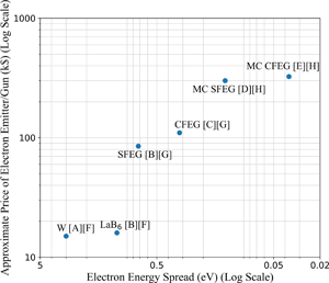
In order to give context to the financial aspect of this paper, Figure 2 compares the electron energy spread of different electron guns and monochromated electron emitters (Kisielowski et al., Reference Kisielowski, Freitag, Bischoff, Van Lin, Lazar, Knippels, Tiemeijer, Van Der Stam, Von Harrach, Stekelenburg, Haider, Uhlemann, Müller, Hartel, Kabius, Miller, Petrov, Olson, Donchev, Kenik, Lupini, Bentley, Pennycook, Anderson, Minor, Schmid, Duden, Radmilovic, Ramasse, Watanabe, Erni, Stach, Denes and Dahmen2008; Sawada et al., Reference Sawada, Tanishiro, Ohashi, Tomita, Hosokawa, Kaneyama, Kondo and Takayanagi2009; Stöger-Pollach, Reference Stöger-Pollach2010; Carpenter et al., Reference Carpenter, Xie, Lehner, Aoki, Mardinly, Vahidi, Newman and Ponce2014; Williams & Carter, Reference Williams and Carter2009) versus their approximate cost which was gathered through private communication with the following researchers who have spent years working in the field of electron microscopy: R. Beanland, personal communications, December 7, 2021; G. Nicotra, personal communications, November 29, 2021; D. Muller, personal communications, November 28, 2021. It is a visual representation of our literature findings and emphasizes the differential cost between electron gun configurations.
Fig. 2. A visual representation of the general trends in the price/performance trade-off of a variety of electron guns and monochromators. Further details for all emitters are found in the original literature: [A] Williams & Carter (Reference Williams and Carter2009), [B] Stöger-Pollach (Reference Stöger-Pollach2010), [C] Sawada et al. (Reference Sawada, Tanishiro, Ohashi, Tomita, Hosokawa, Kaneyama, Kondo and Takayanagi2009), [D] Kisielowski et al. (Reference Kisielowski, Freitag, Bischoff, Van Lin, Lazar, Knippels, Tiemeijer, Van Der Stam, Von Harrach, Stekelenburg, Haider, Uhlemann, Müller, Hartel, Kabius, Miller, Petrov, Olson, Donchev, Kenik, Lupini, Bentley, Pennycook, Anderson, Minor, Schmid, Duden, Radmilovic, Ramasse, Watanabe, Erni, Stach, Denes and Dahmen2008), and [E] Carpenter et al. (Reference Carpenter, Xie, Lehner, Aoki, Mardinly, Vahidi, Newman and Ponce2014). Pricing data was collected via personal communications: [F] R. Beanland, December 7, 2021; [G] G. Nicotra, November 29, 2021; and [H] D. Muller, November 28, 2021.
From Figure 2 we see that cold FEGs have the lowest energy spread of all the electron sources but are the most expensive due to their ultra-sharp tips, more complicated set up, and requirement for a more complex pumping system (Franken et al., Reference Franken, Grünewald, Boekema and Stuart2020). Electron monochromators are the most effective but also the most expensive solution to reducing electron energy spread and one must still consider the loss of electron dose when they are employed. These variations in price could be considered when comparing the simulated images produced by the different equipment.
Materials and Methods
The energy spread of an electron source can be measured from the full width half maximum (FWHM) of the electron energy loss spectroscopy (EELS) zero loss peak (ZLP). For our analysis this was taken as 650 meV for a Schottky FEG (Grogger et al., Reference Grogger, Hofer, Kothleitner and Schaffer2008) and 287 meV for a cold FEG (Hachtel et al., Reference Hachtel, Lupini and Idrobo2018). Hachtel et al. (Reference Hachtel, Lupini and Idrobo2018) demonstrated that as a monochromator reduces the electron energy spread, the FWHM of the ZLP decreases; this in turn decreases the integral of the ZLP, indicating a reduction of the total beam current. The beam current reduction of a Schottky and cold FEG from various levels of monochromation was determined from the EELS ZLP of a Schottky FEG [Fig. 3 of (Grogger et al., Reference Grogger, Hofer, Kothleitner and Schaffer2008)] and a cold FEG [Fig. 2a of (Hachtel et al., Reference Hachtel, Lupini and Idrobo2018)], respectively. The remaining beam current for both FEGs with increasing levels of monochromation was calculated by integrating the graph at their respective FWHM of various energy spreads (see Supplementary Figure 1). These values were then used in the following image simulations.
STEM image simulations were performed using the PRISM algorithm implemented in the Prismatic 2.0 package (DaCosta et al., Reference DaCosta, Brown, Pelz, Rakowski, Barber, O'Donovan, McBean, Jones, Ciston, Scott and Ophus2021), an open source GPU-accelerated STEM simulation software. Across our simulations the appropriate wavelength was used corresponding to each acceleration voltage, as scattering cross section also depends on wavelength our simulations necessarily reflect changes in scattering with voltage. The simulation was averaged across 10 frozen phonons to account for thermal diffuse scattering. Using post-processing techniques chromatic aberration, finite source size, and Poisson noise were included in the simulated images. The chromatic aberration can be approximated by taking a weighted average of a spread of defocused images (Aarholt et al., Reference Aarholt, Frodason and Prytz2020), and has been previously successfully executed using multislice (Sasaki et al., Reference Sasaki, Sawada, Okunishi, Hosokawa, Kaneyama, Kondo, Kimoto and Suenaga2012). The defocus values and weightings were chosen from a Gaussian distribution (see Supplementary Figure 2).
The annular dark-field (ADF) simulations used a detector angle range of 40–150 mrad. Of course, in simulations a range of any number of apertures could have been used. A practical microscope in the lab does not have a continuum of options, so a fixed-size aperture with a probe semi-angle of 28 mrad was chosen. The pixel dwell time was taken as 40 μs (Mullarkey et al., Reference Mullarkey, Downing and Jones2021), giving a total exposure time of ~8.35 s for each simulated image. Previously, Prismatic assumed a point source for electron emission at the gun, but in this work a source-size contribution was added. A mixed Gaussian-Cauchy distribution has been shown to accurately describe source effects (Verbeeck et al., Reference Verbeeck, Béché and Van den Broek2012). However, as we are primarily interested in the trends across our data, a purely Gaussian distribution was chosen for simplicity where the source size (after demagnification) determines the FWHM of the Gaussian distribution. The source size for a Schottky FEG is lifetime dependent (Lebeau et al., Reference Lebeau, Findlay, Wang, Jacobson, Allen and Stemmer2009) and a mid-range estimate of 80 pm was chosen from literature (Lebeau et al., Reference Lebeau, Findlay, Allen and Stemmer2008, Reference Lebeau, Findlay, Wang, Jacobson, Allen and Stemmer2009; Erni et al., Reference Erni, Rossell, Kisielowski and Dahmen2009; Brown et al., Reference Brown, Chen, Weyland, Ophus, Ciston, Allen and Findlay2018). For the cold FEG a mid-range estimate of 40 pm was chosen (Jones & Nellist, Reference Jones and Nellist2014; Brown et al., Reference Brown, Ishikawa, Sánchez-Santolino, Lugg, Ikuhara, Allen and Shibata2017; Sánchez-Santolino et al., Reference Sánchez-Santolino, Lugg, Seki, Ishikawa, Findlay, Kohno, Kanitani, Tanaka, Tomiya, Ikuhara and Shibata2018). This source size contribution is added as a 2D convolution post-processing step to the ADF image. We are also aware that changing monochromator dispersion has some effect on effective source size however there is insufficient data on this in the literature so it was not modeled here. Finally, Poisson noise was added after scaling the relative dose by 1.5× in the case of the cold FEG due to its higher brightness (Xin et al., Reference Xin, Kynoch, Han, Liang, Lee, Larbalestier, Su, Nagahata, Aoki and Longo2013; Williams & Carter, Reference Williams and Carter2009).
Metallic nanoparticles are susceptible to knock-on damage (Azcárate et al., Reference Azcárate, Fonticelli and Zelaya2017). This makes them a very relevant candidate for optimizing STEM performance at lower voltages. The simulations were of a gold nanoparticle on a carbon support imaged at three different low voltages (E = 15, 30, and 60 keV). These acceleration voltages were arbitrarily chosen to span a wide range of low-voltage imaging conditions, however the reader can adapt this value for their own particular sample. Here we considered only a C s-corrected STEM where the C s coefficient was fully corrected (0 mm). The simulations for the Schottky FEG were evaluated for eleven different electron energy spreads spanning the range from severe monochromation to its usual electron energy spread (ΔE = 25, 50, 75, 110, 150, 200, 250, 287, 400, 500, and 650 meV), while the cold FEG was only evaluated for eight different energy spreads (ΔE = 25, 50, 75, 110, 150, 200, 250, and 287 meV) as it had an initial lower energy spread of 287 meV. Our methodology does not aim to reproduce the energy spread of any particular monochromator, rather the energy spreads used in the simulation are spaced to reveal the underlying trends. The reader may wish to follow this methodology for their own particular energy spreads. These simulations were also run for four different OL C c coefficients to represent a variety of OLs available during tendering [C c = 1.1, 1.8, and 3.0 mm (JEOL Ltd, 2004)] as well as, for comparison, a STEM with a chromatic aberration corrector installed (C c = 0 mm) (see Supplementary Figures 3 and 4). As this is a simulation study, sample damage and scan distortion effects (Jones et al., Reference Jones, Yang, Pennycook, Marshall, Van Aert, Browning, Castell and Nellist2015; Van Aert et al., Reference Van Aert, De Backer, Jones, Martinez, Béché and Nellist2019) aren't included, so the images produced will only show a best case scenario. However as this is consistent across all the data sets investigated it is still a fair comparison between all the simulations.
Since these were simulated images, the known ground truth was used to calculate the image signal-to-noise ratios (SNR) using
 $${\rm SNR} = \displaystyle{{{\rm RMS}( {{\rm signal}\;-\;{\rm mean}( {{\rm signal}} ) } ) } \over {{\rm RMS}( {{\rm noise}\;-{\rm \;mean}( {{\rm noise}} ) } ) }}, $$
where RMS is the root mean square. The signal is defined as the noise-free ground truth image with source size but not Poisson noise or chromatic defocus blur, while the noise is defined as the difference once the signal is subtracted from the image inclusive of dose and chromatic effects. As SNR was chosen as a proxy for resolvability, noise and chromatic blur are both together considered to be deleterious behaviours. Both the signal and the noise are mean-subtracted to look at the undulations in the signal which give rise to the visual contrast. More details regarding the SNR calculation can be found in the Supplementary material. These SNRs were plotted to determine the optimum energy spread for a STEM with either a Schottky or cold FEG based on its C c coefficient and the acceleration voltage. The same methodology we present here can be used by the reader to determine the optimum energy spread reduction for their STEM.
Results and Discussion
Figures 3a and 3b show a subset of our simulated gold nanoparticle imaged at 30 and 60 keV for a STEM with a Schottky and cold FEG respectively. Each row of images has been simulated with different OL C c coefficients and the columns show the simulations run at several of the different energy spreads of the monochromated Schottky and cold FEG. The ΔE = 650 meV and ΔE = 287 meV represent a sample imaged with the energy spread of an unmonochromated Schottky and cold FEG in Figures 3a and 3b respectively, while the ΔE = 287, 150, and 25 meV in Figure 3a represent the sample imaged at three different levels of monochromation for the Schottky FEG. In Figure 3b only two levels of monochromation to ΔE = 150 and 25 meV of the cold FEG are shown. For the full panel of all eleven and eight energy spreads at all the different acceleration voltages for the Schottky and cold FEG, please refer to Supplementary Figures 3–8. Comparing the different ΔE for the two FEGs at different levels of monochromation allows us to determine the optimum ΔE when imaging, while still considering the loss of beam current due to the monochromator.

Fig. 3. Simulated Au nanoparticle images at (a) E = 30 keV with a Schottky FEG and (b) E = 60 keV with a cold FEG, both at various levels of monochromation. For each column ΔE = 25, 150, and 287 meV, and an additional 650 meV column for the Schottky. The C c coefficient for each row is 0, 1.1, 1.8, and 3.0 mm from top to bottom, respectively. Scale bar is 15 Å.
One should note that the first three columns of the Schottky FEG in Figure 3a correspond to the same energy width for the corresponding columns of the cold FEG in Figure 3b. This highlights the two extremes of our simulations; the Schottky FEG with its lower brightness at a lower acceleration voltage of 30 kV and the cold FEG with its higher brightness at a higher acceleration voltage of 60 kV. Qualitatively examining Figure 3a we see that the energy spread of a Schottky FEG (650 meV) in a STEM with a high C c coefficient of 3.0 mm (bottom right corner) produces the lowest SNR out of the combinations. However, in the monochromated beam with the lowest energy spread (25 meV) and C c coefficient of 0.0 mm (top left corner), the beam current is attenuated, and the SNR suffers due to increased Poisson noise, meaning purely minimizing both your energy spread and C c coefficient is not necessarily the optimal configuration. The same trend is seen for the 60 and 15 keV images in the Supplementary material except for the overall increased effect of chromatic aberration in the 15keV image due to the reduced electron energy, resulting in reduced SNR. With the continual improvement in instrumentation, and an increased interest in Transmission SEM (Klein et al., Reference Klein, Buhr and Georg Frase2012), as well as ultra-low-voltage imaging in the STEM (Sasaki et al., Reference Sasaki, Sawada, Hosokawa, Sato and Suenaga2014) analysis of voltages as low as 15 kV may be an interesting future research direction. A similar trend is seen for the cold FEG in Figure 3b and its images at lower acceleration voltages in Supplementary Figures 7 and 8.
To quantitatively analyze the simulations equation (2) was used to calculate the image SNRs as a function of energy spread for the four different C c coefficients in Figure 4 at 60, 30 and 15 keV. Examining the right-hand side of the Schottky FEG C c = 3.0 mm curve in Figure 4a we see that at the large energy spread of the Schottky FEG (650 meV), the SNR is low. As this energy spread, and consequently the effect of chromatic aberration for the monochromated Schottky FEG, decreases from right to left, the SNR increases until it reaches a maximum SNR. Conversely, as ΔE decreases, the beam current is further attenuated, reducing the number of electrons. Therefore for high levels of beam attenuation, this results in a lower SNR which decreases at a rate of the square root of the number of electrons due to the increasing effect of Poisson noise (Craven, Reference Craven and Brydson2011). The curves for the two lower Schottky FEG C c coefficients in Figure 4a follow the same trend except that their SNR peaks are shifted to higher electron energy spreads as their lower C c coefficients mean chromatic aberration will have less of an effect on their SNR. As a result, their maximum SNR is also higher. Naturally, when chromatic aberration has been corrected for (C c = 0 mm), there is no reduction in SNR due to chromatic aberration as ΔE increases, so the SNR increases continuously as the dose is increased. The datapoints at ΔE = 650 meV and ΔE = 287 meV for the Schottky and cold FEG respectively may lie off the trendlines for all C c values as they are the unmonochromated and should be considered separately since any degree of monochromation will reduce the current heavily from the exclusion of the tails of the ZLPs.

Fig. 4. Signal-to-noise ratio as a function of electron energy spread at (a) E = 60, (b) 30, and (c) 15 keV, respectively. The filled-in markers represent the Schottky FEG datapoints, while the unfilled markers represent the cold FEG datapoints. Note that the datapoint marked with an asterisk lies off the trend as it is unmonochromated, whereas any form of monochromation will reduce the current heavily from the exclusion of the tails. This is not as visible for larger values of C c as these are dominated by chromatic effects.
The monochromated cold FEG also follows the same trend as the monochromated Schottky FEG for different energy spreads and C c coefficients, however overall it has higher SNR values. This occurs because the cold FEG is brighter than a Schottky FEG (Xin et al., Reference Xin, Kynoch, Han, Liang, Lee, Larbalestier, Su, Nagahata, Aoki and Longo2013; Williams & Carter, Reference Williams and Carter2009) and as its initial energy spread is also inherently lower, monochromating both to an equivalent energy spread results in a lower beam current reduction for the cold FEG. The same trend in Figure 4a is followed for Figures 4b and 4c for the 30 and 15 keV images for both the Schottky and the cold FEG respectively, the only difference being that their SNRs are lower as they are imaged at a lower acceleration voltage and therefore chromatic aberration will have an even more deleterious effect on their SNR.
Figure 4 therefore reveals a clear optimum for each parameter set. In Figure 4a, for example, if your STEM had a Schottky FEG and a C c coefficient of 1.1 mm, the maximum SNR would be at a ΔE of approximately 190 meV, while it would be approximately 150 meV if your STEM had a cold FEG. If the C c coefficient was 3.0 mm however the ΔE would be required to be approximately 90 and 60 meV to achieve the maximum SNR for a Schottky and cold FEG respectively. As mentioned previously changing monochromator dispersion will have some effect on effective source size and this effect might cause the peak in this plot to shift by a small amount but the overall conclusion where we expect to find a peak is valid.
Analyzing the trends across the non-hardware C c-corrected configurations, and where tilt range is not needed for the particular experiment, we find that a STEM with a high resolution OL with a small C c coefficient would be recommended. However, in a mixed-use facility which requires in situ or tomography capabilities, equipping a pole piece with a very small gap may not be an option therefore installing a monochromator may be necessary and the associated condition of cost may be unavoidable. Anecdotally this is what we see in the community from the two dominant microscope manufacturers, with low-voltage (S)TEM of metallic nanoparticles often being performed on Ultra High Resolution (UHR) pole-piece/cold FEG machines, while in situ experimentalists might prefer a wide gapped monochromated machines.
From Figure 4 it is also evident that the chromatic aberration-corrected STEM (C c = 0 mm) will produce the highest SNR in comparison to any uncorrected STEM due to the lack of effect of chromatic aberration. However as stated previously C c correctors are very expensive to install into the microscope and require extensive training for the STEM operator, these factors should therefore be carefully considered when deliberating their purchase.
It is also clear from Figure 4 that a monochromated cold FEG will always produce a higher SNR value than a monochromated Schottky FEG at the same C c coefficient and energy spread due to its higher brightness. However, it is interesting to note that the SNR of a low C c coefficient pole piece without monochromation at the energy spread of a cold FEG (287 meV) is still greater than that of a monochromated Schottky FEG STEM with a high C c coefficient pole piece. Therefore, if you have a high resolution pole piece with a small C c coefficient, and if an energy spread of 287 meV is acceptable, you do not necessarily have to invest in a monochromator to produce high SNR images at low voltages but could simply upgrade your Schottky FEG (ΔE = 650 meV) to a cold FEG (ΔE = 287 meV) to deliver the necessary performance.
The reader could apply this same method of analyzing the performance of their microscope via the SNR of simulated images at various electron energy spreads for their own microscope's OL C c coefficient as well as choice of apertures and other instrument-dependent values. In this way the method followed here can be applied to more novel samples or the reader's own instrument, and an informed choice of what upgrade could be installed into their own particular machine to improve its performance could be achieved.
Conclusion
Despite C s correctors now becoming increasingly commonplace in many modern facilities, low-voltage imaging of sensitive materials remains a characterization challenge. While determining the cost of any one component of a STEM is somewhat obfuscated, we find a strong correlation between the cost of a given illumination system and its energy spread performance. Here across four example hardware configurations and for three example acceleration voltages we show the expected signal-to-noise ratio as a function of varying degrees of monochromation for both a Schottky (ΔE ≤ 650 meV) and cold FEG (ΔE ≤ 287 meV). These plots show that for systems with a higher intrinsic C c, more severe monochromation is indicated whilst for lower intrinsic C c, a slightly less monochromated beam with more beam current yields a greater SNR. The plots also demonstrate that for a beam monochromated to any given energy spread, the cold FEG will always outperform the equivalent Schottky FEG due to increased brightness. Finally, for any given type of gun, a lower C c (smaller gap) pole piece will always give a higher SNR, but there may be other trade-offs accompanying the decision for example a decrease in EDX collection efficiency. With the escalating cost of flagship instrumentation, microscopists should be encouraged to look again at the various routes to achieve comparable levels of performance and with this methodology we offer a potential tool to do so. Revisiting concepts from decades past regarding pole piece geometry and emitter choice may be merited.
Supplementary material
To view supplementary material for this article, please visit https://doi.org/10.1017/S1431927622000277.
Acknowledgments
The authors acknowledge the support of the Advanced Microscopy Laboratory of the Centre for Research on Adaptive Nanostructures and Nanodevices (CRANN). F.Q. is financially supported by the Provost's Project Award, P.M.B. is supported by the School of Physics and the Advanced Materials and BioEngineering Research (AMBER) Centre (Grant No. 17/RC-PhD/3477), P.O.D. was supported by a School of Physics Summer Undergraduate Research Experience (SURE) scholarship. J.J.P.P. is supported by an SFI grant (Grant No. 19/FFP/6813), and L.J. is supported by an SFI/Royal Society Fellowship (Grant No. URF/RI/191637).


 Open access