


No CrossRef data available.
Article contents
Characterization of the Source/Drain Region in Mos Devices by Scanning Transmission Electron Microscopy
Published online by Cambridge University Press: 02 July 2020
Abstract
The advancement of metal-oxide-semiconductor (MOS) technology towards sub- 100nm device dimensions presents several technical difficulties. Nanoscaling in MOS devices is specifically governed by difficulties in the formation of ultrashallow junctions for the source/drain regions with the requirement of low resistance and low leakage currents. The use of a silicide (forming Schottky contacts at the source and drain) instead of the conventional ion implanted Si for the contacts allows a reduction in the contact area to be made, due to lower serial resistance per unit area of the silicide. According to the specific contact resistance dependence on the Schottky barrier height (ΦSB) and active dopant concentration (ND),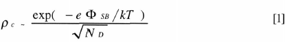
- Type
- Quantitative STEM: Imaging and EELS Analysis Honoring the Contributions of John Silcox (Organized by P. Batson, C. Chen and D. Muller)
- Information
- Copyright
- Copyright © Microscopy Society of America 2001
References
references
8. This work is sponsored by NSF grant # DMR-9733895 and a gift from Intel corporationGoogle Scholar