


No CrossRef data available.
Article contents
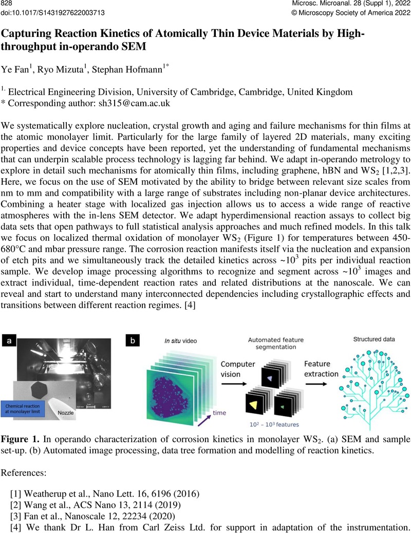
Capturing Reaction Kinetics of Atomically Thin Device Materials by High-throughput in-operando SEM
Published online by Cambridge University Press: 22 July 2022
Abstract
An abstract is not available for this content so a preview has been provided. As you have access to this content, a full PDF is available via the ‘Save PDF’ action button.
- Type
- From Operando Microcell Experiments to Bulk Devices
- Information
- Copyright
- Copyright © Microscopy Society of America 2022
References
We thank Dr L. Han from Carl Zeiss Ltd. for support in adaptation of the instrumentation.Google Scholar
 You have
Access
You have
Access