


Crossref Citations
This article has been cited by the following publications. This list is generated based on data provided by Crossref.
Paterson, Gary W.
Webster, Robert W. H.
Ross, Andrew
Paton, Kirsty A.
Macgregor, Thomas A.
McGrouther, Damien
MacLaren, Ian
and
Nord, Magnus
2020.
Fast Pixelated Detectors in Scanning Transmission Electron Microscopy. Part II: Post-Acquisition Data Processing, Visualization, and Structural Characterization.
Microscopy and Microanalysis,
Vol. 26,
Issue. 5,
p.
944.
Nord, Magnus
Webster, Robert W. H.
Paton, Kirsty A.
McVitie, Stephen
McGrouther, Damien
MacLaren, Ian
and
Paterson, Gary W.
2020.
Fast Pixelated Detectors in Scanning Transmission Electron Microscopy. Part I: Data Acquisition, Live Processing, and Storage.
Microscopy and Microanalysis,
Vol. 26,
Issue. 4,
p.
653.
Haindl, Silvia
Nikolaev, Sergey
Sato, Michiko
Sasase, Masato
and
MacLaren, Ian
2021.
Engineering of Fe-pnictide heterointerfaces by electrostatic principles.
NPG Asia Materials,
Vol. 13,
Issue. 1,
Levin, Barnaby D A
2021.
Direct detectors and their applications in electron microscopy for materials science.
Journal of Physics: Materials,
Vol. 4,
Issue. 4,
p.
042005.
McCartan, Shane J.
Calisir, Ilkan
Paterson, Gary W.
Webster, Robert W. H.
Macgregor, Thomas A.
Hall, David A.
and
MacLaren, Ian
2021.
Correlative chemical and structural nanocharacterization of a pseudo‐binary 0.75Bi(Fe0.97Ti0.03)O3‐0.25BaTiO3 ceramic.
Journal of the American Ceramic Society,
Vol. 104,
Issue. 5,
p.
2388.
Jeong, Jiwon
Cautaerts, Niels
Dehm, Gerhard
and
Liebscher, Christian H.
2021.
Automated Crystal Orientation Mapping by Precession Electron Diffraction-Assisted Four-Dimensional Scanning Transmission Electron Microscopy Using a Scintillator-Based CMOS Detector.
Microscopy and Microanalysis,
Vol. 27,
Issue. 5,
p.
1102.
Ophus, Colin
Zeltmann, Steven E.
Bruefach, Alexandra
Rakowski, Alexander
Savitzky, Benjamin H.
Minor, Andrew M.
and
Scott, Mary C.
2022.
Automated Crystal Orientation Mapping in py4DSTEM using Sparse Correlation Matching.
Microscopy and Microanalysis,
Vol. 28,
Issue. 2,
p.
390.
Sickel, Julian
Asbach, Marcel
Gammer, Christoph
Bratschitsch, Rudolf
and
Kohl, Helmut
2022.
Quantitative Strain and Topography Mapping of 2D Materials Using Nanobeam Electron Diffraction.
Microscopy and Microanalysis,
Vol. 28,
Issue. 3,
p.
701.
Esser, Bryan D
and
Etheridge, Joanne
2022.
A Facile Method for Improving Quantitative 4D-STEM.
Microscopy and Microanalysis,
Vol. 28,
Issue. S1,
p.
384.
Harrison, Patrick
Zhou, Xuyang
Das, Saurabh Mohan
Lhuissier, Pierre
Liebscher, Christian H.
Herbig, Michael
Ludwig, Wolfgang
and
Rauch, Edgar F.
2022.
Reconstructing dual-phase nanometer scale grains within a pearlitic steel tip in 3D through 4D-scanning precession electron diffraction tomography and automated crystal orientation mapping.
Ultramicroscopy,
Vol. 238,
Issue. ,
p.
113536.
2022.
Principles of Electron Optics, Volume 3.
p.
1869.
Wu, Mingjian
Stroppa, Daniel G
Pelz, Philipp
and
Spiecker, Erdmann
2023.
Using a fast hybrid pixel detector for dose-efficient diffraction imaging beam-sensitive organic molecular thin films.
Journal of Physics: Materials,
Vol. 6,
Issue. 4,
p.
045008.
Hooley, Robert
Morávek, Tomáš
de Menezes, Eduardo Serralta Hurtado
Chandran, Narendraraj
Lu, Jing
and
Narayan, Raman
2023.
Adding Another Dimension to 4D-STEM with EDX-assisted Crystal Orientation and Phase Mapping.
Microscopy and Microanalysis,
Vol. 29,
Issue. Supplement_1,
p.
320.
Corrêa, Leonardo M.
Ortega, Eduardo
Ponce, Arturo
Cotta, Mônica A.
and
Ugarte, Daniel
2024.
High precision orientation mapping from 4D-STEM precession electron diffraction data through quantitative analysis of diffracted intensities.
Ultramicroscopy,
Vol. 259,
Issue. ,
p.
113927.
Thronsen, E.
Bergh, T.
Thorsen, T.I.
Christiansen, E.F.
Frafjord, J.
Crout, P.
van Helvoort, A.T.J.
Midgley, P.A.
and
Holmestad, R.
2024.
Scanning precession electron diffraction data analysis approaches for phase mapping of precipitates in aluminium alloys.
Ultramicroscopy,
Vol. 255,
Issue. ,
p.
113861.
MacLaren, Ian
Frutos‐Myro, Enrique
Zeltmann, Steven
and
Ophus, Colin
2024.
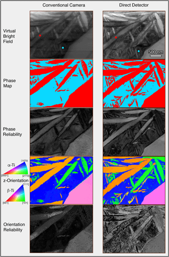
A method for crystallographic mapping of an alpha‐beta titanium alloy with nanometre resolution using scanning precession electron diffraction and open‐source software libraries.
Journal of Microscopy,