Introduction
The family of III-V nitrides (GaN, InGaN, AlGaN) has recently attracted great interest because of their wide spectrum of applications ranging from opto-electronic devices for the blue-ultraviolet spectral region [Reference Nakamura, Senoh, Nagahama, Iwasa, Yamada, Matsushita, Kiyoku, Sugimoto, Kozaki, Umemoto, Sano and Chocho1] to high-temperature electronic devices [Reference Yoshida and Suzuki2]. A large number of processing steps is required for the III-V nitride device fabrication, for example, reactive ion etching (RIE) or focused ion beam (FIB) etching [Reference Adesida, Youtsey, Ping, Khan, Romano and Bulman3], annealing to achieve a low contact resistance to n-type and p-type GaN [Reference Ren and Manasreh4], annealing to activate the Mg-acceptors for p-doping [Reference Nakamura, Mukai, Senoh and Iwasa5]. The non-invasive monitoring of the processing of III-V nitrides is of great interest to gain good control over the III-V nitride device fabrication. In this paper, we demonstrate the use of Raman scattering to monitor non-invasively the processing of GaN, illustrated on the example of the high-pressure high-temperature annealing of ion-implanted GaN films. Ion-implantation is highly attractive for the integration of III-V nitride devices into circuits, however, introduces severe lattice damage [Reference Zolper, Tan, Williams, Zou, Cockayne, Pearton, Hagerott Crawford and Karlicek6]. Annealing at temperatures in excess of 1300°C is needed to recover the crystalline quality of ion-implanted GaN films. AlN cap layers [Reference Cao, Abernathy, Singh, Pearton, Fu, Sarvepalli, Sekhar, Zolper, Rieger, Han, Drummond, Shul and Wilson7] or high-pressure nitrogen atmospheres [Reference Suski, Jun, Leszcyński, Teisseyre, Strite, Rockett, Pelzmann, Kamp, amd and Ebeling8,Reference Suski, Jun, Leszczyński, Teisseyre, Gryzegory, Porowski, Baranowski, Rocket, Strite, Stonert, Turos, Tan, Williams and Jagadish9] have to be employed to prevent the GaN surface decomposition at such high temperatures. Raman scattering provides information on the vibrational states of GaN, which track noninvasively the crystalline quality and the stress in ion-implanted GaN films. The crystalline quality was determined from the E2 phonon linewidth of GaN, whilst the stress from the E2 phonon frequency [Reference Demangeot, Frandon, Renucci, Briot, Gil and Aulombard10]. We restrict this paper on the monitoring of the crystalline quality and the stress in GaN. Results on the free carrier concentration in ion-implanted GaN films monitored by Raman scattering will be reported elsewhere. High optical efficiency micro-Raman systems nowadays make the recording of Raman spectra with very short integration times possible. Fast feedback on the material properties of III-V nitride layers using Raman scattering is therefore possible.
Experiment
Visible and ultraviolet (UV) micro-Raman spectra were recorded from the top surface of annealed Mg/P-implanted GaN films in backscattering Z(X,.) Z geometry, i.e., unpolarized detection, with 1-2 μm spatial resolution using a visible and an ultraviolet (UV) Renishaw micro-Raman system with the 514nm- and 488nm-line of an Ar+-laser and with the 325nm-line of a HeCd-laser as excitation source, respectively. The spectral resolution of the Raman setup was 2-3cm−1 for all excitation wavelengths used. The GaN films used for this study were 1.5 μm thick, growth by metalorganic chemical vapor deposition (MOCVD) on sapphire (0001) substrates (commercially available - CREE). Mg- and P-ions were implanted into the GaN by a multistep process of increasing the ion energy up to 1MeV. As a result, a uniform (across the whole layer thickness) concentration of Mg and P equivalent to 2×1019cm−3 was achieved [Reference Suski, Jun, Leszczyński, Teisseyre, Gryzegory, Porowski, Baranowski, Rocket, Strite, Stonert, Turos, Tan, Williams and Jagadish9]. The samples were annealed at temperatures ranging from 1200°C to 1500°C in a high-pressure furnace. Pressures of 1-1.5GPa were applied, with purified N2 as the pressure-transmitting medium. Mg pieces were placed in the high-pressure furnace near the sample to provide a magnesium overpressure during the annealing. Un-implanted GaN films (taken from the same wafer as used for the ion-implantation) were annealed under the same conditions as the ion-implanted GaN films for comparison.
Results and Discussion
Figure 1 displays the E2 phonon linewidth of ion-implanted and of un-implanted GaN films obtained (a) under 514nm- and (b) under 325nm-excitation as function of the annealing temperature. The E2 linewidth is a measure for the crystalline quality of the GaN. The results obtained under 514nm-excitation (Figure 1(a)) probe the crystalline quality of the GaN films averaged over the sample layer thickness, those obtained under 325nm-excitation (Figure 1(b)) determine the crystalline quality in a sample surface layer of 1/(2α) =40nm thickness due to the absorption of the laser light in the GaN (α = absorption coefficient at 325nm taken from [Reference Muth, Lee, Shmagin, Kolbas, Casey, Keller, Mishra and DenBaars11]). The E2 linewidth of ion-implanted GaN films decreases with increasing annealing temperature. After 1500°C anneals, it is comparable to the E2 linewidth of as-grown GaN films. No broadening of the E2 phonon linewidth was detectable for annealing temperatures as high as 1500°C under 325nm-excitation. No significant surface degradation occurred therefore during the annealing. For un-implanted GaN films, high-pressure high-temperature annealing results in a decrease of the E2 linewidth for annealing temperatures of 1300-1400°C, however, this is reversed at 1500°C. High-pressure high-temperature annealing restores the crystalline quality of ion-implanted GaN films to a large extent. It also improves the crystalline quality of un-implanted GaN films.

Figure 1. E2 phonon linewidth of ion-implanted and of un-implanted GaN films determined (a) under 514nm- and (b) under 325nm-excitation. The E2 phonon linewidth is a measure for the crystalline quality of the GaN.
The homogeneity of the investigated samples can be estimated by comparing the E2 linewidths determined under 514nm- and 325nm-excitation (Figure 1(a) and (b)). Ion-implanted and un-implanted GaN films annealed at temperatures in excess of 1300°C exhibit a more or less homogeneous crystalline quality throughout the layer thickness. The E2 linewidths determined under 514nm- and under 325nm-excitation agree within the experimental resolution. In contrast to the above, a reduced surface crystalline quality is found in ion-implanted GaN films annealed at 1200°C with an increased E2 linewidth under 325nm-excitation.
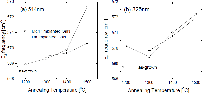
Figure 2 displays the E2 phonon frequency of ion-implanted and of un-implanted GaN films obtained (a) under 514nm- and (b) under 325nm-excitation. The E2 frequency is a measure for the stress in the GaN. Compressive stress emerges and shifts the E2 phonon to larger wavenumbers with increasing annealing temperature. After the 1500°C anneal, a frequency shift of 3.9cm−1 and of 1.5cm−1 is found under 514nm-excitation for ion-implanted and for un-implanted GaN films, respectively, with respect to the sample before ion-implantation and annealing. For ion-implanted GaN films, the E2 frequencies obtained under 514nm- and under 325nm-excitation agree within the experimental resolution. The stress is more or less homogeneous throughout the layer thickness. Inhomogeneous stress is found in un-implanted GaN films annealed at 1500°C with an increased E2 frequency under 325nm-excitation.

Figure 2. E2 phonon frequency of ion-implanted and of un-implanted GaN films as function of the annealing temperature determined (a) under 514nm- and (b) under 325nm-excitation. The E2 phonon frequency is a measure for the stress in the GaN.
Figure 3 compares Raman spectra of as-implanted, un-annealed GaN films recorded under 488nm-excitation at different temperatures. For comparison results obtained under 325nm-excitation at room temperature are also shown. Ion-implantation gives rise to a high-density network of defects [Reference Zolper, Tan, Williams, Zou, Cockayne, Pearton, Hagerott Crawford and Karlicek6] lifting the wavevector conservation of the Raman scattering process (disorder-induced Raman scattering). The Raman spectrum is closely related to the GaN phonon density of states for non-resonant excitation conditions [Reference Cardona, Cardona and Güntherodt12], for example, for an excitation wavelength of 488nm far below the GaN bandgap. The corresponding Raman spectrum recorded at room temperature contains three contributions: a peak at 574cm−1, at 668cm−1 and at 716cm−1. Their linewidth decreases with decreasing temperature, their frequency increases by 1-2cm−1 from 300K to 10K. This temperature-induced frequency shift is in good agreement with values reported for the E2 and the A1(LO) phonons of GaN [Reference Liu, Bursill, Prawer, Nugent, Tong and Zhang13]. Theoretical results on the GaN phonon density of states from Nipko et al. [Reference Nipko, Loong, Balkas and Davis14] calculated using a rigid-ion lattice dynamical model are displayed in Figure 3. We find good agreement between the Raman spectra recorded under 488nm-excitation and the calculated phonon density of states, except for the Raman peak at 668cm−1, which can be attributed to local vibration modes [Reference Limmer, Ritter, Sauer, Menschling, Liu and Rauschenbach15]. Resonance effects can distort the GaN phonon density of states in the Raman spectrum [Reference Cardona, Cardona and Güntherodt12]. This is illustrated in Figure 3 for 325nm-excitation. The UV excitation close to the GaN bandgap resonantly enhances the Raman peak located at 721cm−1 related to the GaN LO phonons. The UV excitation does neither enhance the local vibrational mode at 668cm−1 nor the Raman peak at 574cm−1.

Figure 3. Raman spectra of as-implanted, un-annealed GaN films recorded under 488nm-excitation at different temperatures and recorded under 325nm-excitation at room temperature. The theoretical phonon density of states of GaN is from [Reference Nipko, Loong, Balkas and Davis14].
Micro-Raman scattering allowed us to monitor non-invasively the processing of GaN, namely, to track the crystalline quality and the stress in ion-implanted and in un-implanted GaN films after high-pressure high-temperature annealing. Using different excitation wavelengths GaN properties were probed in the sample surface layer as well as averaged over the sample layer thickness to estimate the homogeneity of the stress and the crystalline quality in the investigated samples. The main result of significance is the nearly full recovery of the crystalline quality of ion-implanted GaN films after high-pressure high-temperature annealing at 1400-1500°C tracked by the decreasing E2 phonon linewidth in Figure 1. Improvements in the crystalline quality were also achieved for un-implanted GaN films by annealing at 1300-1400°C. UV Raman scattering found no significant surface degradation effects during the annealing at temperatures as high as 1500°C. The high nitrogen overpressures proved very effective in preventing the surface decomposition which would normally occur at a temperature of 1000-1200°C [Reference Kuball, Demangeot, Frandon, Renucci, Massies, Grandjean, Aulombard and Briot16,Reference Hayes, Kuball, Bell, Harrison, Korakakis and Foxon17]. Stress is introduced into the GaN layers during the annealing (Figure 2) and shifts the E2 phonon frequency to higher wavenumbers with 2.9cm−1/GPa [Reference Demangeot, Frandon, Renucci, Briot, Gil and Aulombard10]. Annealing at 1300-1500°C therefore introduces a compressive stress of 0.3-0.5GPa in un-implanted GaN films (Figure 2(a)). The increased crystalline quality, i.e., the decreased defect density, in annealed un-implanted GaN films (Figure 1(a)) reduces their ability to relax the stress, which arises from the large lattice mismatch between GaN and the sapphire substrate. Stress also arises from the inclusion of impurities into the GaN crystal lattice such as the Mg and P in the ion-implanted GaN films (Figure 2(a)).
Conclusions
We have investigated the high-pressure high-temperature annealing of ion-implanted and of un-implanted GaN films using micro-Raman spectroscopy. Using ultraviolet (UV) and visible excitation wavelengths the crystalline quality and the stress was monitored in the sample surface layer as well as averaged over the sample layer thickness, respectively. Disorder-induced Raman scattering was used to investigate the GaN phonon density of states. The results illustrate the use of Raman spectroscopy to monitor processing of GaN where fast feedback is required.
Acknowledgements
We acknowledge financial support for the work in Bristol by Renishaw plc (Dr. G.D. Pitt), by EPSRC (grant no. GR/M15590) and by the Royal Society (grant no. 20141). J.M.H. is supported by a CASE studentship from DERA Malvern (Dr. T. Martin). We thank C.K. Loong (Argonne National Laboratory) for providing the theoretical data on the GaN phonon density of states.