Introduction
There is currently an increasing interest in the growth of high quality nitride related materials for fabrication of short-wavelength devices for displays [Reference Amano, Sawasaki, Akasaki and Toyoda1-Reference Nakamura, Mukai and Senoh2]. This has been initiated by use low temperature buffer layers (AlN or GaN) [Reference Amano, Sawasaki, Akasaki and Toyoda1]. Until now, most of the studies for the group III nitrides have dealt with the improvement of films quality, the characterization of physical properties has become an integral part of research for the understanding of material behavior and performance under operating conditions. Numerous accurate tools as transmission electronic microscopy (TEM) [Reference Ponce, Major, Plano and Welsh3], scanning probe microscopy (SCM) [Reference Aktas, Kim, Fan, Boktarev, Salvador, Mohammad, Sverdlov and Morkoç4] techniques are largely used for the qualification of the layers. Furthermore, the increasing need of feedback informations has spurred the development of original characterization methods. In the following, the high sensitivity of prism coupling for the characterization of the interface properties is demonstrated.
Experimental
The AlGaN films were grown on (0001) sapphire substrates at a low pressure using a metalorganic vapor phase epitaxy (MOVPE) apparatus. A low-temperature AlN nucleation layer of thickness 10nm was first deposited on sapphire at 800°C. Growth temperature of the active layers was carried out at 1170°C. Details of the growth procedure were published elsewhere [Reference Omnes, Marenco, Beaumont, de Mierry, Caille and Monoz5].
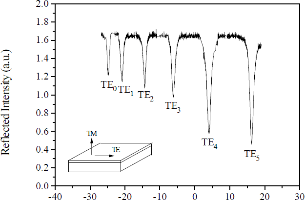
The optical properties of AlGaN / AlN heterostructures were measured by using a guided-wave technique based of the prism coupling. This technique was described in details by Tien et al [Reference Tien, Sanseverino and Martin6]. In short, a He-Ne laser beam emitting at a wavelength of 632.8nm is coupled into the AlGaN layer using a rutile prism (TiO2) through the evanescent field in the air-film gap. By measuring the reflected intensity versus the angle of incidence α, we draw the guided-mode spectrum of the samples (figure 1). With the optical axis normal to the surface, the ordinary and extraordinary modes are respectively excited using transverse electric (TE) and transverse magnetic (TM) polarized light.

Figure 1 Experimental set up of the prism coupling method
The same layers were examined by transmission electron microscopy using cross section samples prepared in the conventional way of mechanical polishing followed by ion milling.
Results
In the TE mode spectrum of the AlGaN films, six sharp reflectivity dips are observed at certain angles α which correspond to the excitation of guided modes (figure 2). These can be identified as the modes TE0 – TE5. Note that six modes have been excited with the TM polarized light. From the angular position of the TE or TM guided-modes, the corresponding effective mode indices are calculated according to


Figure 2 TE coupling curve of the laser beam into epitaxial AlxGa1-xN films.
where Np is the refractive index of the prism, α is the angle of incidence and Ap is the prism angle with respect to the normal.
Using the calculation procedure reported by Ulrich and Torge [Reference Ulrich7], the ordinary refractive index (n0) of AlGaN has been determined as 2.3240±0.004 at 632.8nm. The extraordinary refractive index (ne) obtained from the TM mode data is 2.3648±0.006. The calculated thickness is 1.2±0.01 µm in agreement with the SEM observations.
In order to investigate the film homogeneity in the whole thickness and at the interface, we have reconstructed the refractive index profiles of samples. The approach based on the inverse WKB method usually associated with Wentzel, Kramers and Brillouin, was employed. This method was first proposed by J.M. White [Reference White and Heidrich8] to study the propagation characteristics of single crystal LiNbO3 waveguides, and then improved by K.S. Chiang [Reference Chiang9] for Cu diffused MgO film waveguides. From the knowledge of effective mode indices, the index profile n(x) can be determined by solving the following characteristics equation for mth order mode given by

where n(x) and Nm are respectively the refractive index profile and the effective index of mth order mode, xt(m) is defined as the “ turning point ” according to
Generally, we assumed that the phase shift ϕs at the surface is taken as π/4 and ϕa is approximated to π/2 at the turning point as given by K.S. Chiang et al [Reference Chiang9]. This method was described in detail by Dogheche et al [Reference Dogheche, Belgacem, Rémiens, Ruterana and Omnes10].
From the angular position of modes given in figure 2, the effective mode indices was calculated. The reconstructed refractive index profiles of various samples prepared under optimized process conditions was investigated. As shown in figure 3, a non-abrupt film-substrate interface is observed.

Figure 3 Refractive index profile from a 1.2 µm thick AlGaN thin film using an improved inverse WKB method
Reconstruction of index profiles was investigated for various samples prepared under optimized process conditions. The profile was obtained from the analysis of the TE modes. Figure 3 displays the evolution of the ordinary refractive index as a function of the layer thickness. Three distinct regions are observed. First, the index of refraction is maximum at the film surface (index n0 = 2.3240) and remains constant within the guiding region I. This behavior is synonymous of a homogeneous layer along the whole thickness. Further, in the region III, the index decreases rapidly near the substrate surface. These two regions are observed commonly for step-index thin film structures. In our case, an additional region II is observed in the profile n(x), we denoted a two-time decrease of the index profile. The occurence of fluctuations in the profile and the change in the shape near the substrate surface are indicative of a problem in the growth process. The region II illustrates the existence of a disturbed layer which appeared near the film-substrate interface. In fact, during the early stage of growth, many defects are introduced into the film, which can lead to the islanding and columnar growth. This behavior results in large deterioration of the crystal structure at the interface. In the present study, the interface containing defects manifests itself through the changes of the optical properties of samples. As a consequence, the index of refraction is lowered in the region near the interface. The curve plotted figure 3 shows a thickness of around 60nm where the index profile n(x) is modified, it may related to the extent of this disturbed region. The optical study of interface properties by the reflectivity technique was also described by Shokhovets et al [Reference Shokhovets, Goldhahn, Cimalla, Cheng and Foxon11] for GaN grown on GaAs. In this work, the observed defects are a consequence of the mixing of GaN and GaAs. A thin interlayer with a refractive effective index below that of GaN was found. It was explained as the presence of voids in the interface region which lowers the refractive index in the mixed zone.
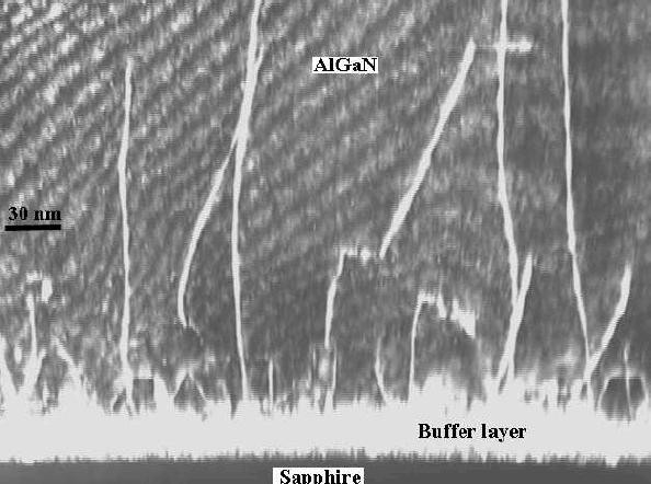
The same AlGaN films were analyzed by transmission electron microscopy (TEM). In fact, the growth of AlGaN films is strongly dependent on the quality of the buffer layer. During the early stages of the growth, many defects are introduced into the film which can lead to islanding and columnar growth. This behavior may result in large deterioration of the crystal structure at the interfaces, leading to high-quality and low-dislocations heteroepitaxial films. The <1010> dark field observations show a mosaic growth, which is more less pronounced depending on the samples. As noticed in figure 4, (0002) weak beam images show a highly defective interfacial layer extends to 60nm, instead of the initial 10nm thickness of the aluminum nitride buffer layer. This area contains also a high density of dislocation loops. The density of dislocation loops decreases drastically beyond the interfacial layer of 60nm.

Figure 4 Cross-sectional 0002 weak beam image of a AlGaN layer grown on sapphire with a 10nm thick-AlN nucleation layer.
This mechanism can be compared to the model of the buffer layer efficiency as proposed by Nakamura et al [Reference Nakamura and Fasol12], where a low-temperature buffer layer of 50nm was estimated to give rise to highly defective layer of 150nm called a semi sound zone. In our case, this zone is confined to the first 60nm. This could be probably one explanation for the refractive index behavior as shown in figure 3.
Conclusion
In conclusion, using a combination of optical characterizations and transmission electron microscopy (TEM) analysis, it is shwn that the growth properties of AlGaN / AlN heterostructures on sapphire can be investigated. A non-destructive prism coupling optical characterization was carried out to determine the waveguide mode informations, i.e. effective mode indices, which are treated through an original iWKB formalism to reconstruct the refractive index profile along the film thickness. There was an evidence of bending effects at the AlGaN/AlN buffer layer interface, extending in a thickness of 60nm. This area correspond exactely to the highly defective layer at the interface which appears to modify the index profile n(x). The results reveal the prospect of determining the relationship between structural and optical properties as a function of composition x for AlxGa1−xN.