


1. Introduction
The wide bandgap semiconductor GaN shows great promise for blue light emitting diodes and ultraviolet laser diodes. To realize such devices it is necessary to obtain thin films with controlled concentrations of impurities. The common dopants for GaN are Mg, Al, Si, Zn, Cd, and In Reference Morkoc, Strite, Gao, Lin, Sverdlov and Burns[1]. Also, H, C, and O can be electrically active elements and the knowledge of their concentration is also of great interest Reference Gauneau, Chapling, Rupert, Salvi and Desconts[2]. It is therefore important to develop methods of analysis for all impurities which may affect device performance. Secondary Ion Mass Spectrometry (SIMS) is a powerful and convenient method for the determination of the distribution and concentration of impurities. It can perform quantitative analysis based on ion implanted standard samples Reference Leta and Morrison[3] and is superior to other techniques with regard to the lateral and depth resolution.
In this study we optimized the analysis conditions to determine detection limits of impurities of interest for controlling the conductivity of GaN films. In-depth analyses of contaminants such as H, C, O is also shown.
2. Experiment
Standard samples were prepared by ion implantation into (0002) GaN films under the conditions listed in Table I. The implantation energy was chosen to obtain a maximum impurity concentration (Rp) depths between 100 − 150 nm to reduce the influence of sub-surface layers. The dose was selected to provide a maximum impurity concentration of ~1 atomic percent to insure a linear dependence of the impurity signal versus concentration (to within <1% Reference Leta and Morrison[3]). The thickness of the GaN films were ≥2 μm to permit the measurement of the implantation distribution to 10ΔRp.
Table I Ion implantation data for the GaN samples

A Cameca IMS 4f instrument was used. The analysis conditions were defined from empirically established principles for AIIIBV semiconductors Reference Wilson, Stevie and Magee[4]. We selected 5.5 keV O2 + primary ions to analyze Mg, Al and In; positive secondary ions were recorded. Cs+ primary ions (E = 5.5 keV) were used for Zn and Cd and CsX+ ions (X = Zn, Cd) were detected. The Si, H, C, O signals were obtained using negative secondary ion registration. Primary current densities of 100 − 1000 μA/cm2 were employed. The sputter rate for GaN was 2 − 10 Å/sec for the various of primary ions.
To eliminate a crater edge effects we chose the field and contrast diaphragms so that only a 60 μm diameter area centered in the 250 μm x 250 μm crater was analyzed.
3. Results and discussion
3.1 Determination of Mg, Al, and In
The calibration characteristics C = f(Iimpurity/Imatrix ion) obtained for each impurity from analyses of the implantation profiles are given in figure 1. The GaN+ signal was chosen as the matrix reference ion. The raw data yielded ion counts per unit time which has been replotted in figure 1 once the total number of integrated counts was correlated with the implantation dose. In such graphs, the detection limit corresponds to the background level of the implantation profile. The main limitation to determining a detection limit in all the cases is bulk contamination of matrix by the analyzed impurity.
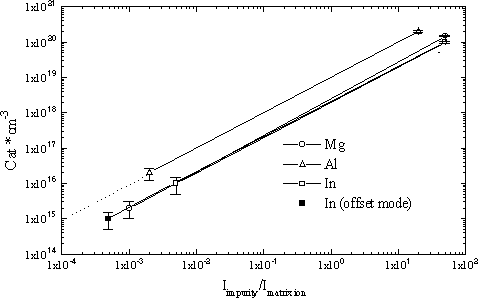
Figure 1. Calibration characteristics of Mg, Al and In impurities in GaN.
Some samples showed initial Mg matrix contamination which could be in the form of local inclusions revealed in our ion images of analyzed area. The detection limit for Mg presented in figure 1 corresponds to the “pure” matrix background level.
Local inclusions were more pronounced when we analyzed for Al (figure 2). We do not discuss the nature of the inclusions in this paper, but we believe their presence explains the high background signal level. Therefore, we believe that it is reasonable to expect that a 1015 atoms/cm3 detection limit for Al (dotted line, figure 1) would be possible in the “pure” matrix case.

Figure 2. Ion image (27Al+) of Al contamination in the GaN-matrix (image field is 150μm).
The detection limit of In is defined by the superposition of the matrix complex ions, such as (71Ga14N2 16O)+, (71Ga28Si16O)+ or (71Ga27Al16O1H)+, and the 115In+ signal. To minimize the influence of the complex ions it is possible to change the secondary accelerating voltage (offset ~ 90 V). This method allows one to discriminate complex ions by means of an energetic slit because they have a more narrow energetic distribution in comparison to monatomic ions. When complex ions are minimized, the In detection limit decreases by one order or magnitude (solid squares, figure 1).
3.2 Determination of Si, Zn and Cd
It is known Reference Gaunean, Chaplain and Rupert[5] that the maximum ion yield of Zn and Cd in GaAs matrix is realized by using cesium primary beam with CsZn+ and CsCd+ secondary ion registration. We have determined that this is also true for the GaN matrix. Our measured detection limits are presented in figure 3, where the 147CsN+ ion current was taken as the matrix signal. The use of O2 + ions on the same standard samples combined with monatomic 64Zn+ and 114Cd+ ion registration gave 5-10 times higher detection limits.

Figure 3. Calibration characteristics of Cd,Zn and Si impurities in GaN.
The determination for Si (figure 3) was realized by analyzing negative secondary ions (28Si−) with the aid of the high mass resolution mode (ΔM/M = 3000). The N2 − matrix signal was taken as the reference. This is a traditional method for optimal Si determination in AIIIBV semiconductors Reference Homma and Ishii[6] Reference Inoue, Sakaki, Yoshina and Yoshioka[7]. The background signal appeared to be one order of magnitude above the detector background due to volume contamination of Si in the GaN matrix. The detection limit is actually much lower than the 10.5 × 10¹⁶ atoms/cm3 represented by the dotted line in figure 3.
It must be mentioned that the high resolution mode is difficult to realize when one must record concentration profiles of several elements simultaneously. In-depth analysis of Si and Mg in GaN can serve as an example. We estimated the Si detection limit at optimal Mg analyzing conditions (O2 + primary beam and 44SiO+ registration) to be only 1018 atoms/cm3. Hence, if it is not necessary to detect very low Si concentrations, it is possible in normal mode operation (ΔM/M ~ 300) to determine the position of a GaN pn junction directly.
3.3 Determination of H, C and O
The high electronegativity of these elements defines the choice of the analytical conditions. To have high sensitivity it is undoubtedly necessary to use Cs+ primary ions to stimulate a high yield of negative secondary ions Reference Wilson, Stevie and Magee[4]. Our dynamic range (Cmax/Cmin) for concentrations of H, C and O is ≤2.1:1, even in experiments with optimal primary beam current density (~250 μA/cm2). Therefore, we present the data most illustratively as implantation profiles (figure 4). The steady trend of the curve is defined by the background level corresponding to the volume contamination of the matrix by the analyzed impurity. We established that the maximum ion yields for H and O the monatomic negative ions, while for C the yield of CN− ions is one order of magnitude higher than that of C−.

Figure 4. Depth profiles of H, C and O in implanted samples.
The reason for the high background signal levels for the gaseous impurities is clearly illustrated in figure 5 which shows ion images of the analyzed areas. The images were obtained under conditions identical to those of the analyses over a 150 μm diamter. Segregation of these impurities to the crystallite boundaries is clearly observed. Carbon forms also incorporations with lack of H and O. We conclude that these impurities are incorporated during the crystal growth. We do not believe that it would be a problem to achieve detection limits for these elements of ~1016 atoms/cm3 because the background level corresponding to the impurity concentration in the matrix is three orders of magnitude higher than the ion detector noise level.

Figure 5. Ion images of H, C and O contaminations in the GaN matrix (a − GaN−, b − H−, c − CN−, d − O−).
4. Conclusions
SIMS experiments were performed to determination appropriate analytical conditions for the analyses of elements commonly used for doping GaN. Analyses of standard implanted samples shows that detection limits down to 1015 atoms/cm3 with dynamic ranges of 103 − 105 (Table II) are possible.
Table II Dynamic range and detection limit of analyzed impurities.

Unfortunately, attempts to achieve low detection limits for N, C and O have failed. We postulate that the measured minimum sensitivities of Cmin ≈ 1018 − 1019 atoms/cm3 are caused by the segregation of these impurities on crystallite boundaries.
Finally, we mentioned that our data collection was complicated by sample charging during the ion bombardment and methods must be employed to minimize this effect.
Acknowledgments
The authors gratefully thank Mr. V. Dmitriev for supplying GaN material and Mr. M. Vatnik for the ion implantation.


