Introduction
GaN materials are very interesting for optoelectronic and microelectronic applications like blue and green LEDs, blue lasers, UV photodetectors, high power and high temperature HEMTs. GaN and its related materials (AlGaN, InGaN, InAlGaN) are most commonly grown, using metal organic vapour phase epitaxy (MOVPE) or molecular beam epitaxy (MBE), on α-Al2O3 substrates. For specific applications like high power transistors, silicon carbide substrates are used because of their higher thermal conductivity. The lattice mismatch remains high in both cases with an advantage for SiC, and hence epitaxial layers suffer from stress induced by the lattice mismatch which results in a very high dislocation density (in the range of 108-1010 cm−2). GaN bulk materials form an attractive solution to circumvent the problems of lattice mismatch encountered in hetero-epitaxy by allowing a perfect lattice-matched epitaxy.
Dry etching of GaN has been extensively investigated using numerous plasma-based machines and sources. High etch rate (1.3 μm/min) was reported using an electron cyclotron resonance (ECR) [Reference Vartuli, Pearton, Lee, Hong, Mackenzie, Abernathy and Shul1]. Conventional reactive ion etching (RIE) generally shows lower etch rates and leads to higher level of induced damages. We have developed a highly chemical reactive ion etching process using a conventional parallel plate reactor. In a previous work [Reference Karouta, Jacobs, Vreugdewater, Melick, Schön, Protzmann and Heuken2] we reported a fourfold increase in etching rate when simply adding SF6 to SiCl4 + Ar. This highly chemical RIE process is based on the choice of the gases used for etching. At a power of 300 Watts we achieved an etch rate of 430 nm/min which is twice the etch rate reported by Feng et al [Reference Feng, Guo, Lu and Chang3] of 210 nm/min at the same power using BCl3 + SF6.
In this paper and after a short description of our RIE process, we shall present the results of our RIE investigation on bulk GaN single crystals. We have compared etch rates and morphology after RIE on Ga- and N-polar surfaces. We also have studied the influence of this RIE process on Schottky diodes made on n-GaN.
Experimental
The plasma machine is a load-locked conventional RF-powered reactor (Oxford Plasmalab 100) with an oil-free pumping system (dry pump + magnetically levitated turbo pump). Silicon nitirde as well photoresist were used for masking. All etch experiments were performed at room temperature. Non-intentionally doped MOVPE-grown GaN on α-Al2O3 (0001) substrates was used to investigate the RIE process as a function of gas flow, RF-power and pressure. The optimized process was used for the study on Ga- and N-polar GaN bulk materials. The etch depth was measured using a Tencor-200 surface profiler while the morphology was characterized qualitatively by scanning electron microscopy (SEM) for the MOVPE-grown GaN and quantitatively by atomic force microscopy (AFM) in the case of bulk GaN.
Etching of MOVPE-grown GaN
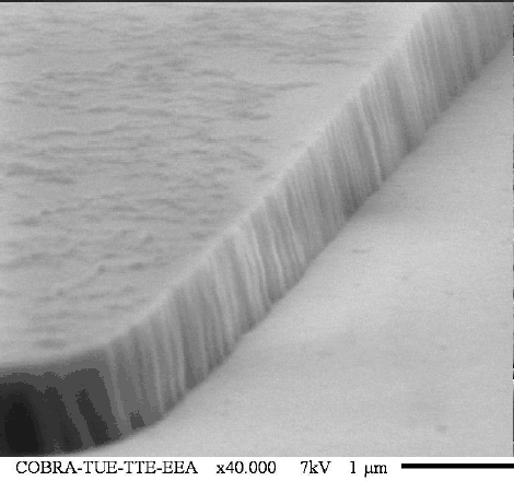
Adding SF6 to the more conventional SiCl4:Ar chemistry has led to a fourfold increase of etch rate. A relatively low power process at 105 Watts using SiCl4:Ar:SF6 (10:10:2 sccm) at 40 or 20 mTorr resulted in an etch rate of ∼100 nm/min instead of 22 nm/min at the same conditions without SF6. The DC bias was ∼ −300 V. Figure 1 shows a typical etched and very smooth GaN surface obtained after 6 minutes of RIE etching.

Figure 1- A SEM photograph of a very smooth surface after RIE using the optimized process at 40 mTorr
Figure 2 clearly shows the influence of SF6 in the RIE process. We believe that etch products, when using SF6, are GaCl3 and NF3. The fact that NF3 is more volatile (boiling point of −129°C) than NCl3 (boiling point around 71°C) explains the fourfold increase of etch rate. Since the etch rate with only argon at 105 W and 40 mTorr was 9 nm/min, this demonstrates the highly chemical property of our RIE process. The decrease in etch rate at higher SF6 flow is presumably due to the fact that more electrons are subject to collisions which do not result in active species. Furthermore, we have achieved a maximum etch rate of 430 nm/min using the same chemistry at 300 W (DC bias around −600V). This is a world record when considering etching results in conventional RIE reactors. Feng et al, have used a comparable chemistry based on BCl3:SF6 and they reported a maximum etch rate of 210 nm/min instead of 50 nm/min without SF6. This fourfold increase of etching rate is remarkably similar to the one we obtained when adding the same fluorinated gas. Adesida et al. [Reference Adesida, Mahajan and Andideh4] have not noticed any change in etch rate (50 nm/min) when adding SiF4 to a SiCl4-based chemistry. These results can be explained by the dissociation energies of the various gases. For instance, these energies are 93.6 and 145.4 kcal/mole for SF6 and SiF4 respectively, while for SiCl4 and BCl3 these values are 94.1 and 110 kcal/mole respectively. It is clear that the SiCl4+SF6 combination has the lowest dissociation energies and hence forms the best choice among these gases.

Figure 2- Effect of SF6 flow on etch rate of GaN.
Etching of bulk GaN crystals
Chemically assisted ion beam etching (CAIBE) using Cl2/Ar (which is dominated by physical sputtering) and RIE using Cl2:Ar:CH4 of bulk GaN were already reported in literature [Reference Schauler, Eberhard, Kirchner, Schwelger, Pelzmann, Kamp, Ebeling, Bertram, Riemann, Christen, Prystawko, Leszczynski, Grzegory and Porowski5,Reference Prystawko, Leszczynski, Beamount, Gibart, Frayssinet and Knap6]. We have used the following RIE process {SiCl4:Ar:SF6 (10:10:2 sccm) at 105 Watts and 40 mTorr} to remove polishing damages from bulk GaN single crystals. It is worth noticing that “standard” MOVPE grown hetero-epitaxial GaN is Ga-polar while GaN single crystal substrates present the advantage of having the two polarities and by simply putting the sample upside down the polarity of homo-epitaxial layer can be changed. The GaN single crystals were grown from liquid gallium saturated with molecular nitrogen at 1600°C and at nitrogen pressure of about 15 kbar [Reference Porowski7].
Because of the small size of the GaN crystals, sapphire blocks of 2×1 mm2 were used for masking in order to measure the etch rates. Two samples of different polarity were simultaneously etched for 6 minutes in each run to realize a realistic comparison and to exclude any reproducibility problems. In addition to the etch rate measurements and SEM photography the morphology of the surface was measured by AFM to determine the RMS roughness (peak-valley differences) in substrates with both polarity.
RIE of Ga-polar GaN substrates
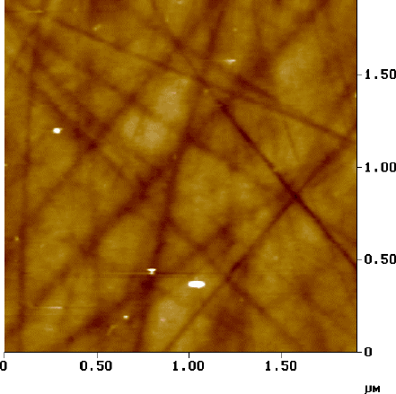
After the mechanical polishing of Ga-polar substrates with diamond paste (0.1 μm final grade), the surface roughness had an RMS value of 20-30 Å. A cleaning in boiling acetone and iso-propanol was carried out before the RIE experiments. Notice that scratches caused by the polishing are clearly visible (fig. 3).

Figure 3- An AFM photograph of Ga-polar surface after mechanical polishing.
After the RIE process an etch rate of 100-110 m/min was measured on these Ga-polar single GaN crystals which is quite similar to that obtained earlier for MOVPE grown hetero-epitaxial GaN.
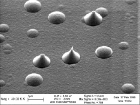
This is quite remarkable since the bulk GaN substrates have much less growth-related defects. This result converge with our previous statement over the highly chemical component of the used RIE process as the etch rate does not depend on density of defects. In conclusion the surface becomes much smoother where RMS value of 4 Å was measured. Thus a clear polishing effect of the Ga-polar surface by RIE is demonstrated. A drawback of this result was the fact that a random distribution of “pillars” has been found (fig. 4-left). After examination of several samples at different RIE conditions we have found that residual organic contaminating particles are the reason of the nucleation of pillars. Performing a 6-minute O2 plasma in the same reactor prior to the RIE process of GaN was effective to get rid of any remnant contamination of the surface and subsequently of the “pillars”. Figure 4-right shows a featureless Ga-polar surface obtained after combined O2 plasma cleaning and RIE. The resulted surface allowed the MOVPE-growth of high quality homo-epitaxial layers [Reference Weyher, Zauner, Brown, Karouta, Wysmolek, Hageman and Porowski8].

Figure 4- A clustering of residual pillars are shown (left) while using an oxygen plasma prior to RIE resulted in a smooth and pillar-free surface (right).
N-polar GaN substrates
The N-polar (000

Figure 5- A rough N-polar surface after RIE with hillocks and mounds.
Besides this overall roughening, large cone-shaped hillocks randomly distributed were present which are probably caused by inversion domain areas. These localized Ga-polar areas are etched slower than the adjacent N-polar surface and hence lead to the formation of the hillocks. Moreover, the increased roughness after RIE can be related to the poor stability of the N-polar surface already observed during high temperature MOVPE [Reference Weyher, Brown, Zauner, Müller, Boothroyd, Foord, Hageman, Humphreys, Larsen, Grzegory and Porowski10].
Electrical behaviour
We have investigated the influence of the RIE process on the electrical properties of GaN layers. Schottky diodes were fabricated on n-type GaN epitaxial layer (2×1017 cm−2). The ohmic contacts were made using Ti/Al (35/115 nm) annealed at 600°C for 30 seconds resulting in a contact resistance of 0.1 Ω.mm. A platinum layer of 100 nm thickness was used for the Schottky contacts. I-V measurements were performed to extract the reverse curent and the ideality factor of the diode. These values were investigated with various pre-treatments of the surface prior to the Schottky metallization. The best partial recovery was achieved when the material was subjected to a short RIE process followed by a HCl dip and a heat treatment at 600°C during 30 seconds. The reverse current and the ideality factor were found to be respectively 4×10⁻⁴ A/mm (−20V), 1.12 (as-grown) and 1×10⁻³ A/mm, 1.12 (after RIE, HCl dip and heat treatment).
Further investigation of the RIE process in conjunction with/or O2-plasma, HCl dip and heat treatment and their influence on the electrical characteristics of GaN and AlGaN layers are undergoing.
Conclusions
A highly chemical reactive ion etching process has been demonstrated based on a combined fluorine and chlorine chemistry. Adding SF6 to SiCl4+Ar resulted in a fourfold increase of etch rate. This RIE process is suitable for removing work damages from Ga-polar substrates and realizing a final polishing of Ga-polar GaN single crystals making them epi-ready.
Acknowledgements
B. Jacobs would like to thank the Netherlands Organisation for Applied Scientific Research (TNO-FEL) for support and J.L.Weyher wishes to thank NATO Scientific Affair Division for the grant HTECH:LG 972924.