


1. Introduction
The family of the III-V nitrides are gradually finding applications in optical devices (LEDs, lasers and detectors) as well as electronic devices Reference Strite and Morkoç[1]. However, the majority of the scientific effort was focused in the growth and characterization of GaN films. Very little effort has been dedicated in the study of the ternary and quarternary alloys. For example, there are conflicting results regarding the bowing parameter in the AlGaN alloys Reference Yoshida, Misawa and Gonda[2] Reference Khan, Skogman, Schulze and Gershenzon[3] Reference Koide, Itoh, Khan, Hiramatu, Sawaki and Akasaki[4] and whether Vegard’s rule is applicable in this system Reference Khan, Skogman, Schulze and Gershenzon[3]. Also there are only limited intentional doping studies Reference Zhang, Kung, Saxler, Walker, Wang and Razeghi[5].
In this paper, we report the growth and Si-doping of AlxGa1−xN alloys with × 0.35 by ECR-MBE.
2. Experimental Methods
The AlGaN films were deposited in a Varian Gen-II MBE unit, equipped with an ASTEX compact ECR plasma source to supply activated nitrogen gas. This deposition method has been described in detail previously Reference Moustakas, Lei and Molnar[6] Reference Moustakas and Molnar[7] Reference Molnar and Moustakas[8] Reference Molnar, Singh and Moustakas[9]. The films were grown on (0001) sapphire substrates, which after degreasing and acid etching, were thermally outgassed and nitridated by exposing to an ECR-nitrogen plasma. This process was found to convert the surface of the substrate to atomically smooth AlN Reference Moustakas, Lei and Molnar[6] Reference Moustakas and Molnar[7] Reference Molnar and Moustakas[8] Reference Molnar, Singh and Moustakas[9]. The films were grown in two temperature steps Reference Moustakas, Lei and Molnar[6] Reference Moustakas and Molnar[7] Reference Molnar and Moustakas[8] Reference Molnar, Singh and Moustakas[9]. A low temperature AlGaN buffer (approximately 300Å thick) was grown at 550-650C and the rest of the film (approximately 1μm thick) was grown at 700-800C at a growth rate typically 0.2μm/hr. Doping was accomplished by subliming silicon at temperatures between 1200-1400°C.
The structure of the films was determined by in-situ 10kV Reflection High Energy Electron Diffraction (RHEED) and X-ray diffraction (XRD), employing Co-Kα radiation, monochromated with a single Ge crystal. The surface morphology and the composition of the films were determined with a JEOL JSM-6100 scanning electron microscope (SEM) equipped with a Kevex detector with a Be-window for energy dispersive x-ray spectroscopy (EDS). EDS measurements at more than 6kV overestimate the concentration of Al in the films due to the contributions from the Al2O3 substrate.
The optical properties of the films (transmission, reflectivity) were measured with Xe-lamp dispersed through a 1m monochromator. The photoluminescence was excited with a 10mW He-Cd laser. The transport coefficients were determined by Hall effect measurements using the Van-der Pauw geometry.
3. Experimental Results
The RHEED pattern of one of the investigated samples is shown in Figure 1. These data are typical of all of the investigated samples. The streaky diffraction pattern is indicative of smooth surface morphologies. The data of Figure 1, which was taken after the sample was cooled to 450°C, indicate clearly 3 × 4 surface reconstruction. The surface morphology and the cross-sectional view of the same film are shown in Figure 2. These data confirm the smooth surface morphology and show no evidence of columnar growth. The lattice constants of the AlGaN alloys were determined by studying the (0002) and (0004) diffractions as shown in Figure 3. The higher XRD orders offer better resolution in measuring the interplanar distance. When the AlGaN film was grown on the top of a GaN film, the lattice constants of the alloys were determined by measuring the relative shift of the AlGaN and GaN peaks. Figure 4 shows the dependence of the lattice constant, c, on AlN mole fraction, determined by EDS measurements. These data indicate that Vegard’s rule is applicable up to 35% Al, which is the extent of the present work. The applicability of Vegard’s rule in this material system is expected since the atomic radii of Al and Ga in covalent bonding are almost the same Reference Kittel[10]. The band gaps of the AlGaN alloys were determined by plotting the square of the optical absorption constant vs photon energy as shown in Figure 5. The band gaps of the same films were also deduced by photoluminescence measurements which show a single peak occurring across the gap (Figure 6), and photoreflectance measurements. Figure 7 shows the dependence of the band gap deduced by the various methods, as a function of AlN mole fraction. These data extend only up to 20% Al and indicate a linear relation between band gap and Al concentration in agreement with the work of Khan and co-workers Reference Khan, Skogman, Schulze and Gershenzon[3]. Reflectivity measurements were also used to determine the index of refraction as a function of wavelength for various AlGaN alloys as shown in Figure 8. The films were doped n-type by varying the Si temperature. AlGaN alloys at various compositions with net carrier concentration varying between 1016 to 1019 cm−3 were obtained. We find that the carrier concentration decreases only slightly with Al content up to about 25% Al (Figure 9). This result differs from those of Zhang and co-workers Reference Zhang, Kung, Saxler, Walker, Wang and Razeghi[5] who report a significant reduction in carrier concentration with Al concentration. Our data indicate that the electron mobility is reduced with Al concentration in the films, a result which is attributed to alloy scattering. Details of the electrical measurement will be presented elsewhere.

Figure 1a. RHEED showing 3×4 surface reconstruction of AlGaN films <1120> azimuth

Figure 1b. RHEED showing 3×4 surface reconstruction of AlGaN films <1100> azimuth

Figure 2a. SEM micrograph of the surface morphology.

Figure 2b. SEM micrograph of the cross sectional view.
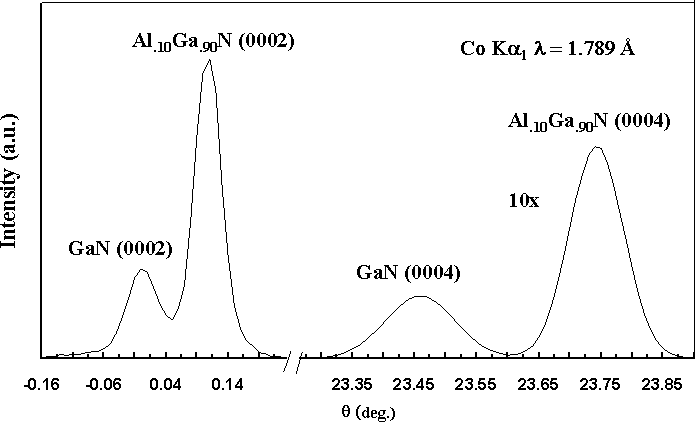
Figure 3. XRD of the (0002) and (0004) peaks of GaN and AlxGa1−xN films
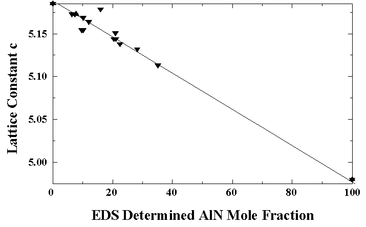
Figure 4. Relationship between lattice constant and AlN mole fraction
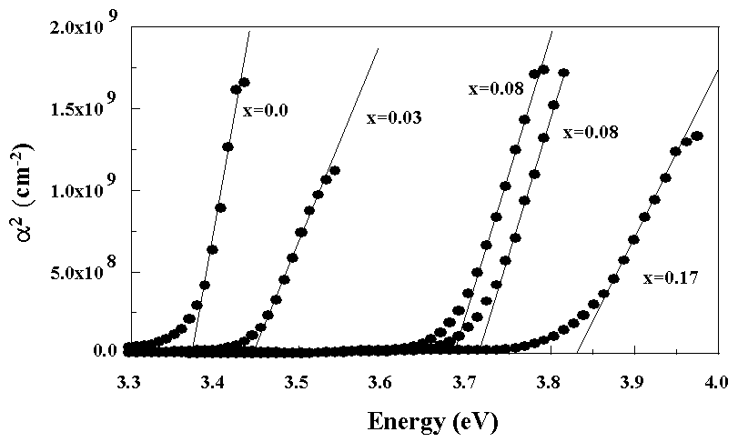
Figure 5. Square of the optical absorption vs photon energy
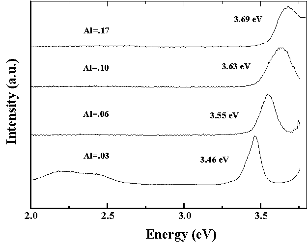
Figure 6. Room temperature photoluminescence of AlxGa1−xN films
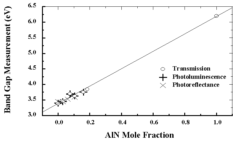
Figure 7. Dependence of band gap on AlN mole fraction
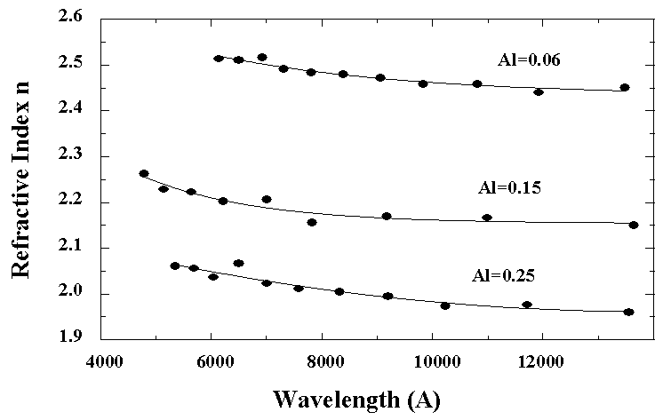
Figure 8. Index of refraction as a function of wavelength
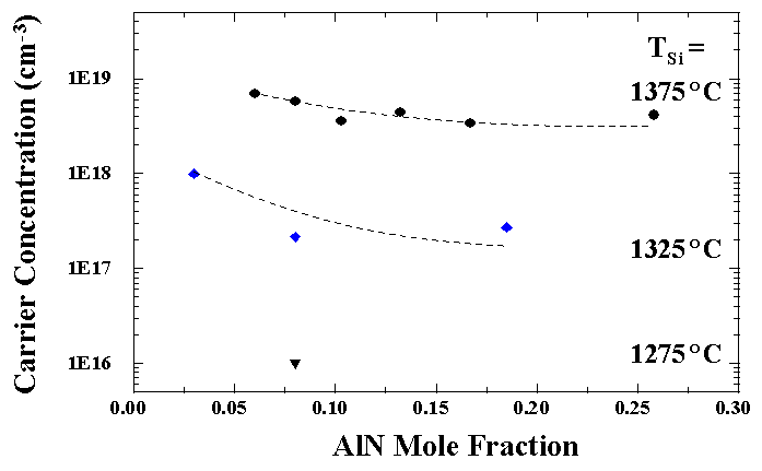
Figure 9. Carrier concentration dependence on AlN mole fraction
4. Conclusions
We found that high quality AlGaN alloys can be grown by the ECR-MBE method at relatively low temperatures (700-800°C). Vegard’s rule was found to be obeyed in the alloy system and the band gap was found to vary linearly with composition. Photoluminescence studies indicate that the primary recombination route occurs across the gap. The films were doped n-type by Si incorporation with net carrier concentration varying from 1016 to 1019 cm−3.Alloying does not significantly affect the carrier concentration up to 25% Al.
Acknowledgments
The authors would like to thank Professor Ludwig for many discussions and use of the X-ray facilities. Many thanks are also expressed to Anlee Krupp for assistance with SEM and EDS analysis. We also acknowledge discussions and help from R. Singh, D. Dharanipal and A. Sampath.
The work was funded by DARPA (Grant No MDA972-95-3-0008)


