10} stacking fault, which has two atomic configurations in wurtzite (Ga,Al,In)N, has been investigated by high resolution electron microscopy and energetic calculations. It originates from steps at the SiC surface and it can form on a flat (0001) sapphire surface. A modified Stillinger-Weber potential was used in order to investigate the relative stability of the two atomic configurations. They have comparable energy in AlN, whereas the 1/2<10
  1>{1
1>{1 Introduction
Extensive research effort is being undertaken on wide band gap of GaN based semiconductors for their very promising device possibilities. Efficient laser diodes have been fabricated for emission in the blue range[Reference Nakamura, Senoh, Nagahama, Iwasa, Yamada, Mitsushita, Kiyoku and Sugimoto1] in layers grown on sapphire by Metal Organic Vapor Epitaxy (MOVPE). The active GaN layers contain large densities of crystallographic defects[Reference Ponce, Bour, Götz, Johnson, Helava, Grzegory, Jun and Porowski2,Reference Vermaut, Ruterana, Nouet, Salvador and Morkoç3], among which, one finds {1
Results
The stacking fault atomic structure
Two atomic models exist in the literature for the { 11
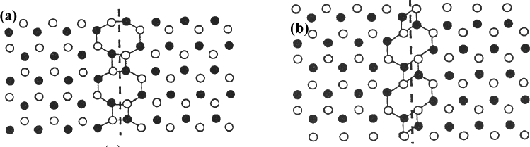
Figure 1. Atomic configurations of the { 11
Formation mechanisms
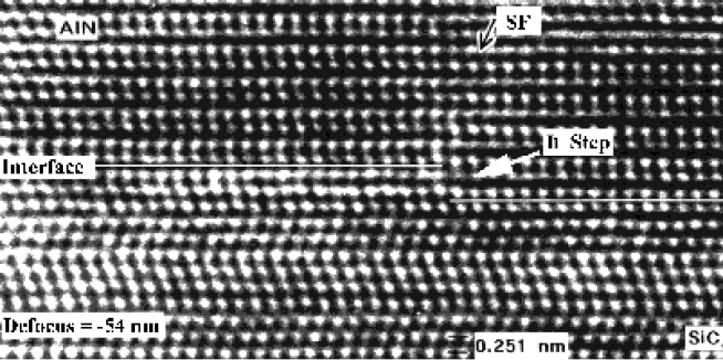
A. Formation on (0001) 6H-SiC surface
The [0001] SiC surface exhibits steps of various heights. If one ignores the mismatch along the c axis which is small, the GaN and SiC can be geometrically consid
A 6H-portion under a step can be decomposed into a faulted 2H stacking, and depending on the type of step, the decomposition may result in a displacement vector between the two crystallites which grow on the adjacent terraces (fig.2). In fact between the two polytypes, the only displacement vectors d which can result from the decomposition are those of the hcp lattice ( the intrinsic I1, RI1 = 1/6 < 20

Figure 2. Generation of a prismatic stacking fault on a I1 type of step on the (0001) surface of 6H-SiC
Table 1. Type of defects forming at an interface step between 2H-GaN and 6H-SiC

B. Growth on (0001) sapphire
The continuation of the two hcp anionic lattices may be described by three types of polyhedra at the interface. They are built with oxygen (O) and nitrogen (N) at their vertices, the metal (M) at the centre: one tetrahedron (3O, M, N) that leads to upward polarity, one tetrahedron (O, M, 3N) and one octahedron (3O, M, 3N) that lead to downward polarity. All these factors are taken into account in order to analyze how the resulting translation can be accommodated in the GaN layers by the formation of planar defects in the epitaxial layer: stacking faults (SF) or inversion domains boundaries (IDB). For the wurtzite structure, three models of IDBs have been proposed[Reference Austerman and Gehman15-Reference Potin, Ruterana and Nouet18].
B.1. Growth on a single terrace
On an oxygen terminated surface, there are four ways to build a hcp stacking of nitrogen atoms, they are related to each other by one of the three stacking fault vectors, RSF, of the wurtzite structure (RI1, RI2 and RE). Since two families of tetrahedral sites are available for the Ga3+ cation, this leads to eight GaN stackings linked by the operator WCE = RSF or WCE = RSF + m with opposite polarities(fig.3). In the case of Al-terminated surface, the number of stackings is reduced to three polyhedra due to the aluminium position in the Al2O3 structure. The systematic analysis of the polyhedra combinations allows to determine the relative proportions of the planar defects induced by the operator WCE. For instance, if the interface polyhedra are exclusively downward tetrahedra, the RSF will be only RI1, and combinations of downward tetrahedra and octahedra lead to the formation of RI1 and RI2 faults in equal proportions which may explain the formation of stacking faults inside the epitaxial layers[Reference Barbaray, Potin, Ruterana and Nouet19-Reference Barbaray, Potin, Ruterana and Nouet21].
B.2. Growth on adjacent terraces
A step, between two terraces on which two GaN islands grow, introduces a translation TS between them. Its component along c axis can be reduced in RE=1/2 <0001> and a residual translation TR. The number of RE is calculated to minimize the absolute value of this residual translation. For instance, the step between two A terraces with a height of c/3 in Al2O3 (0.433 nm) is equivalent in GaN to 0.835 cGaN, or : TS = 2RE + TR = TR with TR = - 0.165 cGaN ≈ cGaN/6. By considering all the steps between A or B terraces (A or B layers of the hcp stacking), the TS translation can be written as : TS = aRE + TR with a = 0 or 1 and TR may take four values with the approximation
As this residual translation is never equal to c/2, it cannot be simply accommodated by the formation of prismatic stacking faults. The operator describing IDBs can be written in order to point out the c/8 translation found inside some of the models in addition to the mirror operation (1). When compared to the residual translation TR, the introduction of the IDB containing the c/8 translation may help in minimizing the shift along c at most of the steps; it is reduced to 1/24 cGaN[Reference Ruterana, Potin, Béré, Barbaray, Nouet, Hairie, Paumier, Botchkarev, Salvador and Morkoç20]. Therefore, in the case of steps, the residual translation cannot be minimized by introducing a stacking fault. During epitaxial growth of GaN layers on (0001) sapphire, the occurrence of basal and prismatic stacking faults is not a straightforward result of the steps at the substrate surface. They form on coalescence of islands whose growth has been initiated with different polyhedra[ Reference Ruterana, Potin, Béré, Barbaray, Nouet, Hairie, Paumier, Botchkarev, Salvador and Morkoç20 ].
Table 2. Residual translation in GaN as a function of the step height in Al2O3


Figure3. Four of the 8 possible stacking of wurtzite (Ga,Al)N on the (0001) sapphire surface, the polyhedra configurations at the interface are shown
Relative stability
The original SW potential is short and it cannot be used in order to predict the values of the non ideal c/a ratio and the vector u which characterizes the displacement along the c axis between the two hcp sublattices in the wurtzite structure. It is unable to reach the third nearest neighbour atom which is responsible of the deviation of c/a ratio from the ideal value. We have added a Gaussian term which was fitted in order to allow the interaction potential to reach the third nearest neighbour. It is given by:
where dij is the bond length between atoms i and j, r1 the center of the Gaussian is situated between the second and third neighbours distances and Δr1 is the width of the Gaussian function. According to the magnitude of r1 and the sign of C, it is possible to adjust the c/a ratio with respect to the ideal value. The potential obtained in the previous section is applied to investigate the atomic structure of the { 11
Table 3. Formation energy in me V/

Conclusion
The two configurations of the stacking fault have already been investigated by conventional electron microscopy, one in AlN and the other in ZnS respectively. They both were found to fold easily from the basal to the prismatic plane of these wurtzite materials. In the basal plane both have the 1/6< 20