


1. Introduction
A wide variety of electron beam irradiation and degradation effects have been reported for GaN-based materials. The electron beam induced effects include increases Reference L Chao, Cargill and Kothandaram[1] or decreases Reference Toth, Fleischer and Phillips[2] in cathodoluminescence (CL) intensities and changes in the spectral distribution of CL emission. The effects have been attributed to electron-beam enhancement of impurity diffusion Reference Toth, Fleischer and Phillips[2], to changes in activated dopant concentrations, to deep levels created by local heating, to increasing uniformity of doping, to creation of vacancies, to annealing out of defects Reference Dassoneville, Amokrane, Sieber and Fravacque[3] , and to absorption by contamination layers Reference Toth, Fleischer and Phillips[2]. Fuller understanding of the mechanisms involved in electron beam irradiation may lead to better control of defects in GaN and to better control of degradation of GaN-based devices.
Carbon complexes can be deposited on a surface irradiated by an electron beam in a scanning electron microscope (SEM). Two possible sources of carbon contamination on a sample in an SEM Reference Campo[4] are vacuum pump oil, particularly for diffusion pumped systems, and the sample itself, since cleaning samples with organic solvents can introduce carbon residues.
The GaN lateral epitaxy overgrowth (LEO) samples described in this paper have been subjected to a series of electron beam irradiation treatments Reference Campo[4] to study effects of irradiation on luminescence. Experiments with these samples show that electron beam irradiation causes a decrease in the intensity of near band edge (NBE) cathodoluminescence that cannot be attributed to absorption by a contamination layer. An alternative explanation is proposed based on charge injection and buildup of internal electric fields.
2. Experimental
GaN samples were grown by MOCVD in Emcore Spectrablue reactors at Emcore Inc. Samples were LEO-grown on sapphire with SiNx masks and GaN buffer layers. A 2 μm thick GaN buffer layer was first grown on a <0001> oriented sapphire substrate, followed by a 100nm thick SiNx mask layer in which patterns of windows were produced by lithographic methods. Sample #1 had a 4 μm wide mask and sample #2 had a 8 μm wide mask. The window openings in the masks were 4 μm wide for both samples. The windows in the mask were oriented along <11
Cathodoluminescence measurements were made in a JEOL JSM-6400 SEM with an Oxford Instruments CF302 CL system, parabolic mirror light collecting optics, a computer-controlled SPEX 340S spectrometer, and a Hamamamtsu-R928 GaAs photomultiplier tube (PMT) detector. The output of the PMT can be used to acquire CL spectra, to measure CL signal strength for a particular wavelength during time, or to form monochromatic CL images. The SEM was equipped with a turbo pump and an ion pump, and the vacuum in the sample chamber was 2.1×10⁻⁶ Torr.
Wavelength dispersive spectroscopy (WDS) measurements were made on a JEOL-Electron Probe X-ray Microanalyzer JXA-733, equipped with independent spectrometers using flow proportional detectors and synthetic multilayer crystals, LDE I and LDE II. Crystal LDE I was used to detect OKα at 23.6 Å and NKα at 31.6 Å, and LDE II was used to detect CKα at 43 Å. The microanalyzer was diffusion pumped, and the vacuum in the sample chamber was 1.8×10⁻⁶ Torr.
Energy dispersive spectroscopy (EDS) measurements were made in the same JEOL-6400 SEM used for the CL experiments. The EDS liquid nitrogen cooled, Si(Li) detector had a thin window, which permitted analysis of light elements. The system could acquire both x-ray spectra and monochromatic x-ray maps.
3. Influence of handling methods on sample contamination
WDS measurements were made on GaN sample #1 to assess contamination from carbon already on the sample Reference Joy, Roming and Goldstein[5] or from carbon deposited on the sample during electron irradiation in the WDS measurement chamber. All samples were rinsed in acetone and air-dried prior to Au-Pd coating. Sample #1 was irradiated in the WDS system with the same experimental conditions as reported previously by Toth et al. Reference Toth, Fleischer and Phillips[2].
WDS wavelength scans with the LDE I crystal from 23 Å to 34 Å requiring 300 seconds were made in spot mode with 25 kV, 300nA electron beam parameters. A wavelength scan from a fresh area is shown as “scan before irradiation” in Figure 1. Wavelength scans in Figure 1 show the OKα peak at 23.6 Å, the NKα peak at 31.6 Å, and other peaks at 25.1 Å and 25.9 Å due to the second order reflections from GaLη and GaLε. Another wavelength scan was made with the same beam parameters on a fresh location from 35 Å to 52 Å using the LDE II crystal to measure the CKα peak. At a nearby location, time based measurements of CKα and OKα signals were made in spot mode with the same beam parameters for 1500 seconds, as shown in Figure 2.
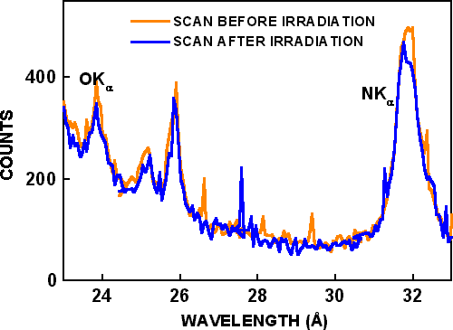
Figure 1. Wavelength dispersive spectroscopy scans. The orange plot shows the scan before irradiation, and blue plot shows the scan after irradiation.
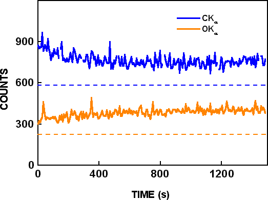
Figure 2. Wavelength dispersive spectroscopy time based scans for CKα and on OKα peaks with 25 KeV and 300 nA electron beam parameters. The dotted lines show the background determined from wavelength scans.
X-ray background intensities from the CKα and OKα wavelength scans are shown by dashed lines in Figure 2. After background subtraction, the CKα signal decreased by 40%, and the OKα signal increased by 80% during electron beam bombardment. A wavelength scan was then made at the same location, and it is shown as “scan after irradiation” in Figure 1. Only very small differences are seen in the two wavelength scans, although they are from different locations and the “scan after irradiation” was made after 1500 seconds of additional electron beam bombardment. In similar experiments conducted by Toth et al. Reference Toth, Fleischer and Phillips[2], the OKα signal increased almost 3 times (270%) during irradiation, and the CKα signal increased over 16 times (1650%) during irradiation. In the time-based scans of Toth et al. Reference Toth, Fleischer and Phillips[2], both CKα and OKα signals increased with time, but CKα decreased and OKα increased with time in the present work with the same residual pressure, beam voltage, beam current and irradiation time. Possible reasons for the different results are described below.
As stated earlier, different carbon contamination rates may result from a variety of reasons Reference Scheuerlein, Taborelli, Hilleret, Brown and Baker[6] such as different levels of hydrocarbon in the residual atmosphere of electron beam analysis instruments or from different levels of hydrocarbon contamination on samples before being placed into the analysis instruments. The experimental results in this section show that our handling methods do not introduce significant carbon build up, and that the CKα signal actually decreases during electron beam irradiation of our samples. The increase in the CKα and in the OKα signals observed by Toth et al. Reference Toth, Fleischer and Phillips[2] could be caused by different methods of handling samples prior to electron beam irradiation. Additionally, the increased OKα signal has been attributed to electromigration of oxygen to the irradiated area Reference Toth, Fleischer and Phillips[2]. However, only the low-defect density LEO region of our samples was irradiated, which is likely to have different impurity concentration and electromigration rates Reference Beaumont, Vennéguès and Gibart[7] from the high defect density blanket films examined by Toth et al. Reference Toth, Fleischer and Phillips[2]. Different grounding conditions could significantly change the electromigration rate of impurities by modifying the built-in electric fields as a result of electron beam irradiation. Our Au-Pd coating and grounding conditions may have decreased the electromigration of oxygen to the irradiated area. Also, the Au-Pd coating may have served as a catalyst to promote C desorption during electron bombardment Reference Joy, Roming and Goldstein[5].
Carbon contamination in vacuum systems has been explained traditionally as resulting from an e-beam activated reaction that decomposes residual hydrocarbons, particularly in diffusion pumped systems Reference Djenizian, Santinacci and Schmuki[8] Reference Folch, Servat, Esteve and Tejada[9]. However, reduced carbon contamination after e-beam irradiation has sometimes also been observed Reference Joy, Roming and Goldstein[5]. Folch et al. Reference Folch, Servat, Esteve and Tejada[9] have proposed that both deposition and desorption phenomena must be considered, and that the combined kinetics of both processes determine the elemental surface composition after e-beam irradiation.
4. Contamination in the CL system
Effects on CL intensities of carbon deposited from residual hydrocarbons in the JEOL-6400 SEM are described in this section. Hydrocarbons are expected to be present in the microscope mainly from vaporization of rotary pump oil. After adsorption of hydrocarbons on the surface of the sample, the electron beam disassociates them into carbon and radicals, and the carbon adheres to the surface Reference Goldstein, Newbury, Echlin, Joy, Roming, Lyman, Fiori and Lifshin[10]. Electron beam bombardment can also cause the carbon to diffuse on the sample surface Reference Scheuerlein, Taborelli, Hilleret, Brown and Baker[6].
Sample #2 was irradiated in cross-section on a window region in spot mode with 20 keV electron beam energy and 35nA beam current for 400 seconds. Two equivalent CL scans were made on similar regions, one to monitor the evolution of the NBE intensity and the other to monitor the evolution of the DL intensity. These scans are shown in Figure 3. Figure 3a shows a 30% decrease of the NBE intensity, and Figure 3b shows only 6% decrease of the DL intensity. Figure 3c shows the wavelength scan on a previously irradiated region, where the NBE intensity (at 365 nm) and the DL intensity (at 560 nm) are similar to those at the end of the time based scans in Figure 3 (a) and (b).
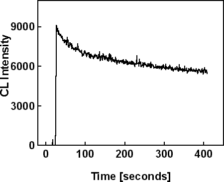
Figure 3a. CL scans in spot mode on the window region of sample #2. Time based scan of NBE emission.

Figure 3b. CL scans in spot mode on the window region of sample #2. Time based scan of DL emission.

Figure 3c. CL scans in spot mode on the window region of sample #2. Wavelength scan after irradiation
To assess the contamination deposited on the sample surface during electron beam irradiation in the JEOL-6400 SEM, EDS measurements were made on sample #2. EDS spectra for a fresh region acquired in spot mode are shown in Figure 4. Electron beam parameters for the initial EDS scan were 10 keV, 2 nA. Another similar region was irradiated in spot mode with 10 keV, 5 nA for 400 seconds. Effects on NBE and DL intensities were similar to those shown in Figure 3a and (b). Next, another EDS spectrum was acquired at the same location, also shown in Figure 4. These EDS scans show the overlapping CKα - NKα - OKα peaks and the GaLα peak, as well as the AuMα peak from the 5 nm-thick coating layer. The CKα, NKα, and OKα peaks are not resolved in the spectrum. However, the CKα - NKα - OKα peak shape show that there was little change in the CKα or OKα peak intensities.
An EDS map was acquired for CKα in scanning mode on the cross-section of sample #2 with 10 keV, 2.6 nA and is shown in Figure 5(a). The size of the scanned region was 13µm × 10µm. A smaller region, 1.5µm × 1.0 µm, was bombarded with a 10 nA electron beam, for 600 seconds while monitoring the near band edge (NBE) emission at 365 nm, as shown in Figure 6. Another EDS map of CKα is shown in Figure 5(c) after irradiation, as well as an SEM image Figure 5(b) after irradiation. The EDS maps were acquired at lower magnification so that the C signals from irradiated and non-irradiated areas could be compared. The irradiated area is shown by the rectangle in Figure 5(b). Most of the carbon signal in Figure 5(a) and Figure 5(c) originates from the top edge of the sample. There is no observable carbon accumulation in the irradiated region, although the NBE intensity was decreased by 70% as seen in Figure 6.

Figure 4. EDS spectra from sample #2 obtained in spot mode on the window region. The spectrum before irradiation was taken on a fresh region. Another spectrum was taken on the irradiated region.

Figure 5. (a) Energy dispersive spectroscopy map at CKα on a fresh region. (b) Secondary electron image of scanned region. The electron beam bombarded area is indicated by the red square on the right wing of the stripe. (c) CKα map including the bombarded area. Window width, visible in (b), is 4 µm.
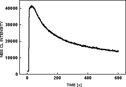
Figure 6. Time based NBE CL scan from a 1.5μm × 1.0 μm region on the LEO region of sample #2.
Both EDS and WDS measurements indicate that no appreciable carbon accumulation occurs during electron beam bombardment, in contrast with the results from Toth et al. Reference Toth, Fleischer and Phillips[2]. The rates of carbon contamination during electron bombardment in microprobes and microscopes depend on the nature and pressure of the residual atmosphere Reference Scheuerlein, Taborelli, Hilleret, Brown and Baker[6]. Less hydrocarbon is expected to be present in the residual atmosphere of turbo pumped systems, like the JEOL-6400 SEM/CL system used in the EDS and CL experiments, than in a diffusion pumped system with the same residual pressure. In the next section, further evidence is given that the decrease in NBE intensity is not caused by carbon absorption.
5. Effect of carbon absorption on NBE and DL luminescence
The decrease of intensity of light passing through a homogeneous layer of uniform thickness t with absorption coefficient α is described by the absorption law Reference Simmons and Potter[11]
where Io is the incident intensity and I is the transmitted intensity.
Experimental absorbance values of carbon at different wavelengths and for different thicknesses have been reported by Toth et al. Reference Toth, Fleischer and Phillips[2]. Absorbance is the product of absorption coefficient and thickness, αt. To explain the 30% decrease of NBE CL intensity shown in Figure 3a by absorption in a built-up carbon contamination layer would require that αt = −ln(I/Io)=0.36. From the absorbance data in ref. Reference Toth, Fleischer and Phillips[2], this would correspond to a carbon layer of thickness t = 20 nm. Let us assume that the NBE-CL intensity decrease observed in our experiments is produced by absorption in a 20 nm-thick carbon layer, and let us quantify the impact that this layer would have on the DL intensity. The absorbance for 20 nm of carbon at the DL emission wavelength, 560 nm, is ~0.3 Reference Toth, Fleischer and Phillips[2]. Substitution of these parameters in Figure 3a predicts a 25% decrease of the DL intensity. However, results of irradiation experiments in Figure 3a and Figure 3b show almost no variation of DL luminescence during time when the NBE luminescence is decreased by 30%. This result provides further support for the decrease in NBE emission not being caused by buildup of a carbon contamination layer.
Irradiation experiments performed by Toth et al. Reference Toth, Fleischer and Phillips[2] showed an enhancement of DL, which was attributed to electromigration of oxygen. This enhancement would have to exceed the decrease of DL intensity from absorption in the growing carbon contamination layer in their case. WDS measurements for our samples show little, Figure 2, or no, Figure 1, increase in oxygen concentration caused by electron beam bombardment. Toth et al. Reference Toth, Fleischer and Phillips[2] reported a four times increase in oxygen concentration. The reasons for the difference between our results and those in ref. Reference Toth, Fleischer and Phillips[2] are unclear, but it could be due to our samples being coated and grounded.
6. Conclusions
The time-based WDS scans from LEO-GaN do not show carbon increase. From the absence of carbon build up in WDS and EDS measurements, and from the observation that DL intensity decreases are much smaller than NBE intensity decreases, we conclude that the decrease of the NBE signal with time is not due to carbon contamination in our CL experiments. Variations on the NBE-CL signal could be associated with the generation of defects during electron beam bombardment or with effects of electric fields generated by charge trapping. These mechanisms will be discussed in upcoming papers.


