Hostname: page-component-8448b6f56d-xtgtn Total loading time: 0 Render date: 2024-04-24T06:27:43.545Z Has data issue: false hasContentIssue false

Novel growth mode of solid–liquid–solid (SLS) silica nanowires

Published online by Cambridge University Press:  23 June 2011

Jae Ho Lee
Affiliation:
College of Nanoscale Science and Engineering, University at Albany—State University of New York, Albany, New York 12205
Michael A. Carpenter
Affiliation:
College of Nanoscale Science and Engineering, University at Albany—State University of New York, Albany, New York 12205
Robert E. Geer*
Affiliation:
College of Nanoscale Science and Engineering, University at Albany—State University of New York, Albany, New York 12205
*
a)Address all correspondence to this author. e-mail: RGeer@uamail.albany.edu
Get access

Abstract

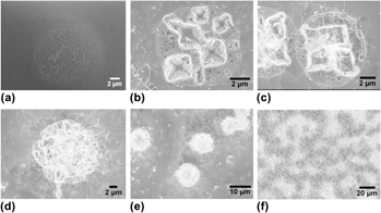
A novel and previously unreported, high temperature solid–liquid–solid (SLS) silica nanowire (NW) growth mode has been observed and investigated. In this mode, SLS NW nucleation and subsequent growth was uniquely promoted by—and coupled to—the formation of thermally etched pyramidal pits in the Si substrate that formed during a high temperature anneal phase before the onset of SLS NW formation. The silicon oxide-mediated thermal pit formation process enhanced Si transport to Au–Si alloy droplets directly adjacent to the pyramidal pits. Consequently, SLS NW nucleation and growth was preferentially promoted at the pit edges. The promotion of SLS NW growth by the pyramidal pits resulted in the observation of SLS NW “blooms” at the pit locations. Subsequent NW growth, occurring both at the pit sites and from Au–Si alloy droplets distributed across the planar surfaces of the Si wafer, eventually occluded the pits. This newly observed process is termed as “thermal pit-assisted growth.”

Type
Articles
Copyright
Copyright © Materials Research Society 2011

Access options

Get access to the full version of this content by using one of the access options below. (Log in options will check for institutional or personal access. Content may require purchase if you do not have access.)

References

REFERENCES

1.Morales, A.M. and Lieber, C.M.: A laser ablation method for the synthesis of crystalline semiconductor nanowires. Science 279, 208 (1998).CrossRefGoogle ScholarPubMed
2.Lu, W. and Lieber, C.M.: Nanoelectronics from the bottom up. Nat. Mater. 6, 841 (2007).CrossRefGoogle ScholarPubMed
3.Colli, A., Fasoli, A., Beecher, P., Servati, P., Pisana, S., Fu, Y., Flewitt, A.J., Milne, W.I., Robertson, J., Ducati, C., De Franceschi, S., Hofmann, S., and Ferrari, A.C.: Thermal and chemical vapor deposition of Si nanowires: Shape control, dispersion, and electrical properties. J. Appl. Phys. 102, 034302 (2007).CrossRefGoogle Scholar
4.Wu, Y., Xiang, J., Yang, C., Lu, W., and Lieber, C.M.: Single-crystal metallic nanowires and metal/semiconductor nanowire heterostructures. Nature 430, 61 (2004).CrossRefGoogle ScholarPubMed
5.Zhang, Y.F., Tang, Y.H., Wang, N., Yu, D.P., Lee, C.S., Bello, I., and Lee, S.T.: Silicon nanowires prepared by laser ablation at high temperature. Appl. Phys. Lett. 721, 835 (1998).Google Scholar
6.Zakharov, N.D., Werner, P., Gerth, G., Schubert, L., Sokolov, L., and Gösele, U.: Growth phenomena of Si and Si/Ge nanowires on Si (111) by molecular beam epitaxy. J. Cryst. Growth 290, 6 (2006).CrossRefGoogle Scholar
7.Yu, D.P., Bai, Z.G., Ding, Y., Hang, Q.L., Zhang, H.Z., Wang, J.J., Zou, Y.H., Qian, W., Xiong, G.C., Zhou, H.T., and Feng, S.Q.: Nanoscale silicon wires synthesized using simple physical evaporation. Appl. Phys. Lett. 72, 3458 (1998).CrossRefGoogle Scholar
8.Westwater, J., Gosain, D.P., Tomiya, S., Usui, S., and Ruda, H.: Growth of silicon nanowires via gold/silane vapor–liquid–solid reaction. J. Vac. Sci. Technol., B 15, 554 (1997).CrossRefGoogle Scholar
9.Cui, Y., Lauhon, L.J., Gudiksen, M.S., Wang, J., and Lieber, C.M.: Diameter-controlled synthesis of single-crystal silicon nanowires. Appl. Phys. Lett. 78, 2214 (2001).CrossRefGoogle Scholar
10.Hochbaum, A.I., Fan, R., He, R., and Yang, P.: Controlled growth of Si nanowire arrays for device integration. Nano Lett. 5, 457 (2005).CrossRefGoogle ScholarPubMed
11.Paulose, M., Varghese, O.K., and Grimes, C.A.: Synthesis of gold-silica composite nanowires through solid-liquid-solid phase growth. J. Nanosci. Nanotechnol. 3, 341 (2003).CrossRefGoogle ScholarPubMed
12.Yan, H.F., Xing, Y.J., Hang, Q.L., Yu, D.P., Wang, Y.P., Xu, J., Xi, Z.H., and Feng, S.Q.: Growth of amorphous silicon nanowires via a solid–liquid–solid mechanism. Chem. Phys. Lett. 323, 224 (2000).CrossRefGoogle Scholar
13.Wagner, R.S. and Ellis, W.C.: Vapor-liquid-solid mechanism of single crystal growth. Appl. Phys. Lett. 4, 89 (1964).CrossRefGoogle Scholar
14.Givargizov, E.I.: Fundamental aspects of VLS growth. J. Cryst. Growth 31, 20 (1975).CrossRefGoogle Scholar
15.Zhang, R.Q., Lifshitz, Y., and Lee, S.T.: Oxide-assisted growth of semiconducting nanowires. Adv. Mater. 15, 635 (2003).CrossRefGoogle Scholar
16.Zhang, R.Q., Chu, T.S., Cheung, H.F., Wang, N., and Lee, S.T.: Mechanism of oxide-assisted nucleation and growth of silicon nanostructures. Mater. Sci. Eng., C 16, 31 (2001).CrossRefGoogle Scholar
17.Zhang, R.Q., Chu, T.S., Cheung, H.F., Wang, N., and Lee, S.T.: High reactivity of silicon suboxide clusters. Phys. Rev. B 64, 113304 (2001).CrossRefGoogle Scholar
18.Lee, J.H., Rogers, P.H., Carpenter, M.A., Eisenbraun, E.T., Xue, Y., and Geer, R.E.: Synthesis and properties of templated Si-based nanowires for electrical transport, in Proceedings of Eighth IEEE Conference on Nanotechnology, IEEE NANO ’08, Arlington, TX, 2008, p. 584.Google Scholar
19.Sekhar, P.K., Ramgir, N.S., Joshi, R.K., and Bhansali, S.: Selective growth of silica nanowires using an Au catalyst for optical recognition of interleukin-10. Nanotechnology 19, 245502 (2008).CrossRefGoogle ScholarPubMed
20.Kim, J.H., An, H.H., Woo, H.J., and Yoon, C.S.: The growth mechanism for silicon oxide nanowires synthesized from an Au nanoparticle/polyimide/Si thin film stack. Nanotechnology 19, 125604 (2008).CrossRefGoogle ScholarPubMed
21.Ueda, K. and Yoshimura, M.: Formation of micromeshes by nickel silicide. Thin Solid Films 464, 208 (2004).CrossRefGoogle Scholar
22.Chang, C.-C. and Shen, P.: Thermal-etching development of α-Zn2SiO4 polycrystals: Effects of lattice imperfections, Mn-dopant and capillary force. Mater. Sci. Eng., A 288, 42 (2000).CrossRefGoogle Scholar
23.Reisman, A., Edwards, S.T., and Smith, P.L.: On the thermal etching of silicon. J. Electrochem. Soc. 135, 2848 (1988).CrossRefGoogle Scholar
24.Reisman, A., Temple, D., and Smith, P.L.: Further comments on the thermal etching of silicon: The surface morphology of (100), (111) and (110) wafers in the temperature range 900°-1150°C. J. Electrochem. Soc. 137, 284 (1990).CrossRefGoogle Scholar
25.Yazdi, G.R., Syvajarvi, M., and Yakimova, R.: Formation of needle-like and columnar structures of AlN. J. Cryst. Growth 300, 130 (2007).CrossRefGoogle Scholar
26.Futagami, M. and Hamazaki, M.: Thermal etching of a (100) silicon surface. Jpn. J. Appl. Phys. 21, 1782 (1982).CrossRefGoogle Scholar
27.Wang, C.Y., Chan, L.H., Xiao, D.Q., Lin, T.C., and Shiha, H.C.: Mechanism of solid-liquid-solid on the silicon oxide nanowire growth. J. Vac. Sci. Technol., B 24, 613 (2006).CrossRefGoogle Scholar
28.Elechiguerra, J.L., Manriquez, J.A., and Yacaman, M.J.: Growth of amorphous SiO2 nanowires on Si using a Pd/Au thin film as a catalyst. Appl. Phys. A Mater. Sci. Process. 79, 461 (2004).CrossRefGoogle Scholar
29.Rubloff, G.W., Tromp, R.M., van Loenen, E.J., Balk, P., and LeGoues, F.K.: Summary Abstract: High temperature decomposition of SiO2 at the Si/SiO2 interface. J. Vac. Sci. Technol., A 4, 1024 (1986).CrossRefGoogle Scholar
30.Tromp, R., Rubloff, G.W., Balk, P., and LeGoues, F.K.: High-temperature SiO2 decomposition at the SiO2/Si interface. Phys. Rev. Lett. 55, 2332 (1985).CrossRefGoogle ScholarPubMed
31.Suzuki, T.: Effect of annealing a silicon wafer in argon with a very low oxygen partial pressure. J. Appl. Phys. 88, 6881 (2000).CrossRefGoogle Scholar
32.Suzuki, T.: Relation between the suppression of the generation of stacking faults and the mechanism of silicon oxidation during annealing under argon containing oxygen. J. Appl. Phys. 88, 1141 (2000).CrossRefGoogle Scholar
33.Suzuki, T.: Oxygen partial pressure dependence of suppressing oxidation-induced stacking fault generation in argon ambient annealing including oxygen and HCl. Appl. Surf. Sci. 180, 168 (2001).CrossRefGoogle Scholar
34.Surdu-Boba, C.C., Sullivana, J.L., Saieda, S.O., Layberrya, R., and Aflorib, M.: Surface compositional changes in GaAs subjected to argon plasma treatment. Appl. Surf. Sci. 202, 183 (2002).CrossRefGoogle Scholar
35.Pan, Z.W., Dai, Z.R., Ma, C., and Wang, Z.L.: Molten gallium as a catalyst for the large-scale growth of highly aligned silica nanowires. J. Am. Chem. Soc. 124, 1817 (2002).CrossRefGoogle ScholarPubMed