


I. INTRODUCTION
Solar-assisted hydrogen production via water splitting by integrated semiconductor based photoelectrochemical systems holds great promise as a cost-effective, environmentally benign energy concept and has been attracting keen interest among many research groups. Reference Miller1,Reference Grimes, Varghese and Ranjan2 Recently, the development of photoelectrodes has been extensively pushed forward, which has led to a vast variety of photoelectrode material systems for water splitting. Reference Li, Luo, Zhang, Feng and Zou3 Efficient conversion of solar energy into a chemical fuel in the form of hydrogen requires photoelectrodes, which generate a photovoltage well above 1.23 V, which is the minimum potential difference to drive the water splitting reactions (disregarding overpotential losses) at a high photocurrent, which defines the amount of produced molecular hydrogen. Reference Weber and Dignam4,Reference Nozik5 To date, solar-to-hydrogen efficiencies for integrated water splitting devices over 10% efficiency have been reported only for expensive and chemical unstable III–V photoelectrode materials in two-junction devices Reference Khaselev and Turner6–Reference Licht, Wang, Mukerji, Soga, Umeno and Tributsch8 or photovoltaic-electrolysis devices based on CIGS (CuIn x Ga1−x Se2). Reference Jacobsson, Fjällström, Sahlberg, Edoff and Edvinsson9 Among alternative candidates, thin film silicon-based photoelectrodes have strongly emerged in recent years. Reference Abdi, Han, Smets, Zeman, Dam and van de Krol10–Reference Calvet, Murugasen, Klett, Kaiser, Jaegermann, Finger, Hoch, Blug and Busse15 In fact, silicon-based thin film technology presents a promising pathway to sustainable solar hydrogen production due to its earth abundance, low cost, and nontoxicity. Reference Shah16
Whereas former studies, listed above, Reference Abdi, Han, Smets, Zeman, Dam and van de Krol10–Reference Rocheleau, Miller and Misra14 exclusively focused on thin film amorphous silicon multijunction devices for water splitting, this study reports on the development and utilization of thin film silicon tandem junction photocathodes made of hydrogenated amorphous silicon (a-Si:H) and hydrogenated microcrystalline silicon (µc-Si:H). In contrast to a-Si:H/a-Si:H tandem junction solar cells, which suffer from rather low photocurrents, the combination of a-Si:H and µc-Si:H in tandem junction devices allows for a more efficient utilization of the solar spectrum and therefore for the generation of higher photocurrents. Additionally, a-Si:H/µc-Si:H tandem devices show less light induced degradation than its all-amorphous counterparts. Reference Keppner, Meier, Torres, Fischer and Shah17,Reference Klein, Finger, Carius, Dylla, Rech, Grimm, Houben and Stutzmann18 However, as a-Si:H has a higher electronic band gap than µc-Si:H, the photovoltage is increased for amorphous silicon multijunctions. Accordingly, there is a tradeoff between high photovoltages and high photocurrents.
To close this high photovoltage/high photocurrent gap, the purpose of this study is to develop a-Si:H/µc-Si:H tandem devices focusing on the improvement of the open-circuit voltage (V OC) without significantly impairing the short-circuit current (J SC), and thus the conversion efficiency of the device. To do so, we first investigated the ways to increase V OC in µc-Si:H single junction solar cells and subsequently implemented µc-Si:H subcells with improved V OC in tandem junction a-Si:H/µc-Si:H cells. The improvement in the performance of single junction μc-Si:H solar cells was conducted by the following routes: (i) variation in the intrinsic µc-Si:H absorber layer thickness; (ii) control of the SiH4 flow during deposition of the intrinsic µc-Si:H absorber layer, aiming to maintain a low crystallinity growth across the entire i-layer; and (iii) incorporation of an intrinsic amorphous buffer layer at the n–i interface of the µc-Si:H solar cell. As a result, V OC of the µc-Si:H single junction solar cells could considerably be improved by around 100 mV up to a value of 580 mV.
Furthermore, based on (photo-)electrochemical experiments, the performance of the developed a-Si:H/µc-Si:H tandem junction photocathodes was evaluated with respect to the hydrogen evolution reaction (HER) and compared to an a-Si:H/a-Si:H photocathode.
II. EXPERIMENTAL DETAILS
A. Preparation of a-Si:H and µc-Si:H layers and solar cells
All thin film silicon layers (a-Si:H and µc-Si:H) were deposited by a plasma enhanced chemical vapor deposition technique in a multi chamber system. For the intrinsic absorber layers, a mixture of silane (SiH4) and hydrogen (H2) gases was used. For the n- and p-type layers, trimethylborane (TMB), methane (CH4) and phosphine (PH3) gases were added to the silane–hydrogen mixture. µc-Si:H solar cells were fabricated with an µc-Si:H p-type layer, an intrinsic µc-Si:H absorber layer and an a-Si:H n-type layer. For µc-Si:H p-type and intrinsic layer depositions, an excitation frequency of 94.7 MHz was applied. For all a-Si:H layers, an excitation frequency of 13.56 MHz was applied. Single junction and tandem junction solar cells were made in a p–i–n and in a p–i–n–p–i–n superstrate configurations, respectively, with a sputtered zinc oxide/silver (ZnO:Al/Ag) reflecting rear contact Reference Böttler, Smirnov, Hüpkes and Finger19 defining the area (1 cm2) of the individual cells. For the a-Si:H/µc-Si:H tandem device, the absorber layer thickness of the µc-Si:H bottom cell was varied between 450 and 1300 nm and the a-Si:H top cell thickness was accordingly adjusted between 400 and 100 nm with a silane concentration (SC) of 4%, defined as the ratio between the SiH4 flow and the total gas flow. The p- and n-type layers are the same for all fabricated solar cells and are deposited at a substrate temperature (T S) of 180 °C. The substrate temperature for the µc-Si:H and a-Si:H absorber layers was 180 and 130 °C, respectively. Reference Urbain, Wilken, Smirnov, Astakhov, Lambertz, Becker, Rau, Ziegler, Kaiser, Jaegermann and Finger20 Amorphous intrinsic buffer layers were deposited with a SC of 10% and a T S of 180 °C. Single and tandem junction solar cells were deposited on 100 cm2 textured aluminum-doped ZnO coated glass substrates. Figure 1 schematically shows the a-Si:H/µc-Si:H tandem junction solar cell configuration used in the photovoltaic (PV) arrangement. For the photoelectrochemical arrangement, 50 nm of platinum was deposited on the ZnO:Al/Ag back contact by electron beam evaporation. This layer is intended to act as a catalyst on the electrolyte side.

FIG. 1. Schematic drawing of the layer stack of a-Si:H/µc-Si:H tandem solar cells.
B. Characterization of materials and solar cells
The structural properties of intrinsic μc-Si:H absorber layers were probed using Raman spectroscopy (λ = 532 nm and λ = 488). The ratio of integrated intensities attributed to crystalline and amorphous regions, I C RS = I C/(I C + I a), was used as semiquantitative value of the crystalline volume fraction. Reference Houben, Luysberg, Hapke, Carius, Finger and Wagner21 Samples were characterized either by a laser beam (λ = 532) directed on the as-produced sample, or, for selected samples, the Raman intensity ratio depth profile of the structure of the intrinsic absorber layer along the growth axis was determined by a gradient etching method (λ = 488 nm). Reference Köhler, Schicho, Wolfrum, Gordijn, Pust and Carius22,Reference Smirnov, Das, Melle, Lambertz, Hülsbeck, Carius and Finger23 Here, Raman scattering measurements were carried out on slantwise etched craters through the solar cell structure.
Solar cells were characterized by current–voltage (J–V) measurements at standard test conditions (AM 1.5 G, 100 mW/cm2, 25 °C) illumination using a double source (Class A) AM 1.5 sun simulator. Furthermore, spectral response measurements [quantum efficiency (QE)] of the tandem solar cells were measured using a monochromator as a light source in the wave length range between 300 and 1100 nm. The top and bottom cell QEs were separately determined using a spectrally filtered bias light from a tungsten lamp. Additional details on QE setup can be found in Ref. Reference Lambertz, Smirnov, Merdzhanova, Ding, Haas, Jost, Schropp, Finger and Rau24.
C. Photoelectrochemical measurements
The photoelectrochemical performance of the photocathodes was evaluated at room temperature in an aqueous 0.1 M sulfuric acid (H2SO4) solution using a three-electrode configuration. Reference Gary25 The potential of the working electrode was controlled by a potentiostat (Metrohm, µAutolab Type III). White light photocurrent measurements were performed under simulated AM1.5 solar illumination (100 mW/cm2) using an Oriel LCS-100 solar simulator (model 94011A, Newport Corporation, Irvine, CA). The solar cells were illuminated through the glass substrate. The setup of the electrochemical cell (type Zahner PECC-2) consists of a Teflon cell body and three electrodes: a working electrode (optimized a-Si:H/µc-Si:H tandem junction solar cell, 8 mm diameter), a coiled platinum wire as a counter electrode, and a Ag/AgCl reference electrode in contact with 3 M sodium chloride (NaCl) [0.268 V versus normal hydrogen electrode (NHE)]. For simplicity, the entire setup will be denoted as a photoelectrochemical cell (PEC) arrangement hereafter. Linear sweep voltammetry measurements were performed with a scan rate of 30 mV s−1. Electrical contact to the transparent conductive oxide (TCO) coated substrate, i.e., the front contact of the solar cell, was made by a silver paste. The PEC arrangement (three-electrode configuration) is schematically shown in Fig. 2.

FIG. 2. Schematic drawing of the photoelectrochemical cell (PEC) measurement setup (three electrode configuration). The components are the a-Si:H/µc-Si:H photocathode (working electrode), the reference electrode (Ag/AgCl electrode in contact with 3 M NaCl), the electrolyte (0.1 M H2SO4), and the counter electrode (coiled platinum wire).
III. RESULTS
A. Solar cells
1. μc-Si:H single junction solar cells
Since the open-circuit voltage (V OC) of μc-Si:H solar cells correlates with the crystallinity of the absorber material, Reference Vetterl, Finger, Carius, Hapke, Houben, Kluth, Lambertz, Mück, Rech and Wagner26–Reference Reynolds, Carius, Finger and Smirnov28 Raman spectroscopy measurements were conducted to estimate the crystalline volume fraction in the samples. The crystallinity I C RS is mainly controllable through the SC ratio during growth of the µc-Si:H layer. As expected, I C RS strongly decreases with increasing SC of the intrinsic µc-Si:H absorber layer (Fig. 3).

FIG. 3. Crystallinity I C RS as a function of the SC of the intrinsic µc-Si:H absorber layer.
a. Thickness variation of the µc-Si:H absorber layer
The performance of the μc-Si:H solar cells, with respect to V OC as a function of the evaluated crystallinity of the absorber layers is presented in Fig. 4 for the solar cells with absorber layer thickness of 1300, 650, and 450 nm. It is well accepted that a decrease in I C RS, i.e., an increase in SC, leads to an increase in V OC because the material increasingly becomes amorphous. Reference Vetterl, Finger, Carius, Hapke, Houben, Kluth, Lambertz, Mück, Rech and Wagner26 For 1300 nm thick μc-Si:H absorber layers, the data show that from I C RS of 15–70% there was only a weak effect on V OC. In this region, the data points show a curvature and V OC varied between 490 and 530 mV with a V OC maximum at 50–40% crystallinity. A strong increase in V OC from 530 to 620 mV was visible only for I C RS values below 15%. A similar trend of V OC as a function of SC for thick μc-Si:H absorber layers above 1.5 µm was already reported in Ref. Reference Droz, Vallat-Sauvain, Bailat, Feitknecht, Meier and Shah27. By reducing the thickness of the μc-Si:H absorber layer to 650 and 450 nm, respectively, the general trend indicates that V OC increases for a given crystallinity as shown in Fig. 4. Overall, our results indicate that thinner absorber layers tend to increase the V OC values, especially in the moderate crystallinity range. For example, at the I C RS of around 30%, V OC increases by around 60 mV (from 500 to 560 mV) when the absorber layer is reduced from 1300 to 450 nm.

FIG. 4. Open-circuit voltage V OC of µc-Si:H single junction solar cells as a function of the crystallinity I C RS of the intrinsic µc-Si:H absorber layers (arrow on the upper x-axis illustrates the corresponding trend for SC). Absorber layer thicknesses of 1300 nm (black triangles), 650 nm (red triangles), and 450 nm (green diamonds) were investigated. The dashed lines serve as a guide to the eye.
b. SiH4 profiling
This section focuses on the growth control of the μc-Si:H absorber layer by means of SiH4 profiling, aiming to obtain a moderate crystallinity (around 50%) absorber layer across the entire i-layer. Previous studies show that profiling could lead to improved performance. Reference van den Donker, Klein, Rech and Finger29,Reference Mai, Klein, Carius, Wolff, Lambertz and Finger30 Figure 5 depicts the Raman intensity ratio depth profile of the structure of the μc-Si:H solar cell along the growth axis, including n- and p-type layers and the intrinsic 1300 nm thick absorber layer (indicated by dashed lines). First, a μc-Si:H solar cell deposited with a standard deposition process (SC of 4.4 and 5%) was investigated. The corresponding SC profile (change of SC during deposition time) is shown in the supplementary material (Fig. S1). The corresponding Raman depth profile is presented in Fig. 5. To a cell thickness of 1000 nm, I C RS consistently increases from 42% to 70% and decreases again down to around 50% from 1000 to 1300 nm. A reduction in crystallinity with increasing μc-Si:H layer thickness was previously observed. Reference Houben, Luysberg, Hapke, Carius, Finger and Wagner21 The steep decrease in I C RS between 1300 and 1350 nm could be attributed to the contribution of the amorphous n-layer. After that, to achieve a homogeneous crystallinity across the absorber layer, the SC was stepwise adjusted during the growth of the intrinsic absorber layer, as shown in Fig. S1. This adapted deposition process will be denoted as SC profiling hereafter. The resulting Raman crystallinity depth profile is presented in Fig. 5 (red squares). The data show that SC profiling could effectively lead to a flattening of the crystallinity profile over the entire cell thickness. It is also evident in Fig. 5 that our approach to maintain a homogeneous crystallinity could be applied in the case of thinner absorber layers. Overall, with this adapted deposition process the efficiency of the solar cell could be enhanced (in the case of particular cells studied here – from 7.2 to 7.6%) along with a gain in V OC (up to 20 mV). The detailed J–V characteristics are shown in Fig. S2, where both solar cells were made with Ag back contact.

FIG. 5. Raman crystallinity depth profile of the μc-Si:H p–i–n solar cell structure without profiling of the SC (standard, black dots) and with profiling of the SC (SC profiling, red squares) during the deposition of the 1300 nm thick intrinsic absorber layer, respectively.
c. Buffer layer incorporation
This section addresses the effects of an intrinsic amorphous buffer layer at the n–i interface on the performance of the μc-Si:H solar cell, as schematically shown in the left part of Fig. 6. Similar approaches led to an increase in V OC and efficiency. Reference Mai, Klein, Carius, Wolff, Lambertz and Finger30,Reference Bugnon, Parascandolo, Hänni, Stuckelberger, Charrière, Despeisse, Meillaud and Ballif31 However, these studies have dealt with microcrystalline buffer layers at the p–i interface. The implementation of an amorphous buffer layer at the p–i interface would however hinder the crystalline growth of the subsequent intrinsic µc-Si:H absorber layer, which is why this concept was not applied in this study. Here, n–i buffer layers of different thicknesses were incorporated in solar cells with different absorber layer thicknesses. The right part of Fig. 6 shows the V OC as a function of the buffer layer thickness (5, 10, 20, 30, 50, 80 nm) for different µc-Si:H absorber layer thicknesses (1300, 650, 450 nm). The buffer layer thickness was estimated based on calculated deposition rate of buffer layer, giving an error in thickness determination within ±10%. The SC of 5% and corresponding crystalline volume fraction were kept constant for all investigated µc-Si:H solar cells. It is apparent that V OC increases with increasing buffer layer thickness. Moreover, as the increase in V OC is more pronounced for thinner cells, the effect of the buffer layer on the solar cell performance seems to increase with decreasing cell thickness. In this regard, it is known that the properties of the solar cell become more interface-sensitive when the cell thickness is reduced. Reference Bugnon, Parascandolo, Hänni, Stuckelberger, Charrière, Despeisse, Meillaud and Ballif31 The 1300 nm thick solar cells exhibit a maximum V OC of 540 mV, 650 nm thick cells exhibit up to 568 mV, and 450 nm thick cells even promote 603 mV. However, as shown in Fig. S3, for solar cells with 80 nm thick buffer layers the conversion efficiency strongly decreases. This is mainly due to poor fill factors, as the current is only slightly affected by an increase of the buffer layer thickness. Overall, the optimal buffer layer thickness, in terms of V OC and efficiency could experimentally be identified for each particular solar cell thickness (Fig. S3). The 1300 nm thick solar cell shows the best performance with a buffer layer thickness of 50 nm, the optimal buffer layer thickness for the 650 nm thick cell was 20 and 5 nm buffer layer thickness exhibited the best performance in the 450 nm thick cell.

FIG. 6. Left: Schematic drawing of the µc-Si:H solar cell with the incorporated n–i buffer layer. Right: Open-circuit voltage V OC of µc-Si:H solar cells as a function of n–i buffer layer thickness (5, 10, 20, 30, 50, 80 nm) for different intrinsic µc-Si:H absorber layer thicknesses (blue circles: 1300 nm, black squares: 650 nm, red triangles: 450 nm). All absorber layers were deposited at a SC of 5%. The maximum error in determination of V oc is below 5 mV.
Figure 7 summarizes all presented routes discussed above and shows the conversion efficiency (η), fill factor (FF), and short-circuit current (J SC) plotted versus V OC for six series of depositions labeled “1300 nm”, “650 nm”, “450 nm”, “1300 nm + SC profiling + buffer layer (50 nm)”, “650 nm + buffer layer (20 nm)”, and “450 nm + buffer layer (5 nm)”. The range of J–V values in each series was obtained by varying the I C RS, i.e., the SC at which the intrinsic absorber layer was deposited, as already discussed in Sec. III. A. 1. a. The measured J–V data at the best-cell V OC are stated in the legend of Fig. 7. For the 1300 nm series, the SC was varied between 4.4 and 6.0%, which resulted in a broad V OC range of 490–620 mV, in agreement with results shown in Fig. 4. Maximum solar energy conversion efficiency is obtained for a V OC of 528 mV, with a SC of 5.0%. Here, a further increase in crystallinity, i.e., decrease of SC to 4.4% could not lead to a further increase of J SC and η slightly decreased along with the FF and V OC. In the range of V OC values between 500 and 530 mV, J SC continuously decreases from around 21 mA/cm2 down to around 10 mA/cm2 with increasing SC from 5.0 to 5.6%. By increasing SC the µc-Si:H material increasingly becomes amorphous and therefore the current decreases. As the FF and V OC mainly remain constant, the conversion efficiency and current trends in this data region resemble. In the 530–620 mV region, SC is varied between 5.6 and 6.0%, inducing a largely amorphous growth of the absorber layer, which is confirmed by the strong increase in V OC. J SC remains at low values between 10 and 8 mA/cm2 and the FF strongly decreases down to 55%, indicating a reduction in the electronic quality of the material. The 650 and 450 nm series depict the PV parameters for decreased absorber layer thicknesses. Compared to the 1300 nm series, both series show increased best-cell V OC values of 545 mV for 650 nm and 565 mV for 450 nm. For the 650 nm series, J SC and FF values stayed nearly constant, resulting in a best conversion efficiency within a series of 8.6%. The SC profiling and buffer layer concept was simultaneously applied for the 1300 nm thick solar cells. Hereby, the best-cell V OC could be increased from 528 to 551 mV, along with an increased conversion efficiency from 8.0 to 8.2%. The 650 nm thin solar cells with an incorporated 20 nm buffer layer exhibit a best-cell V OC of 570 mV with 8.1% conversion efficiency. The highest best-cell V OC of 580 mV is promoted by the 450 nm thin solar cells with a 5 nm buffer layer incorporated. The light absorption of these very thin cells is however rather low, which is in agreement with reduced current density of 17 mA/cm2 and conversion efficiency of 6.7%. Overall, our results indicate that implementation of the concepts described above can lead to improved V OC values over 560 mV without deterioration of other J–V characteristics.

FIG. 7. Solar cell parameters: (a) conversion efficiency η, (b) short-circuit current density J SC, and (c) fill factor FF versus the open-circuit voltage V OC in a 1300 nm (filled squares), a 650 nm (filled triangles), and a 450 nm thick µc-Si:H absorber layer series (filled stars), in a 1300 nm thickness combined with SC profiling and incorporated buffer layer (50 nm) series (open squares), in a 650 nm thickness combined with incorporated buffer layer (20 nm) series (open triangles), and in a 450 nm thickness combined with incorporated buffer layer (5 nm) series (open stars). The trends of the six series around the best-cell V OC are indicated by solid lines as a guide to the eye. The legend summarizes the best-cell parameters for the solar cells indicated by arrows in (a).
2. a-Si:H/μc-Si:H tandem junction solar cells
The optimized, high open circuit voltage, µc-Si:H solar cells from the “1300 nm + SC profiling + buffer layer (50 nm)”, “650 nm + buffer layer (20 nm)”, and “450 nm + buffer layer (5 nm)” series were subsequently utilized as bottom cells in a-Si:H/µc-Si:H tandem junction solar cells. As a reference bottom cell, the “1300 nm” series was used. Various combinations of the top and bottom cells, along with corresponding absorber layer parameters and PV device parameters (η, V OC, FF, J SC) are listed in Table I. Since efficient hydrogen production requires solar cells, i.e., photoelectrodes, which provide a high photocurrent and operate near its maximum power point (MPP) during photoelectrochemical water splitting, the MPP voltage values (V MPP) for all tandem cells are also included in Table I. The corresponding J–V characteristics are presented in Fig. 8.
TABLE I. PV parameters of a-Si:H/µc-Si:H tandem junction solar cells fabricated with different series of µc-Si:H bottom cells and a-Si:H top cells for different SCs and thicknesses. The corresponding current–voltage measurements are depicted in Fig. 8.


FIG. 8. Current–voltage J–V measurements of a-Si:H/µc-Si:H tandem solar cells with different µc-Si:H bottom cells: “1300 nm” reference series (cell A, green curve), “1300 nm + SC profiling + buffer layer (50 nm)” series (cell B, blue curve), “650 nm + buffer layer (20 nm)” series (cell C, red curve), and “450 nm + buffer layer (5 nm)” series (cell D, black curve). The maximum error in determination of η is below 0.2%.
As can be deduced from the data in Table I, the optimization of the µc-Si:H bottom cell could effectively increase the V OC and the V MPP compared to the reference 1300 nm series without significantly impairing device efficiency. For the 650 nm series with incorporated buffer layer (20 nm), the efficiency could even be maintained at 11% (cell C) along with a 100 mV increase in both, V OC and V MPP, and a total tandem cell thickness below 1 µm. The combination of the SC profiling concept and the buffer layer incorporation in the 1300 nm series (cell B) lead to an increase in J SC and V OC of 0.1 mA/cm2 and 80 mV, respectively. However, the fill factor of this tandem cell decreased to 65.6%, resulting in a V MPP of 1184 mV and an overall efficiency of 10.5%. The tandem cell with the 450 nm thin bottom cell with incorporate buffer layer (cell D) exhibited the highest V OC and FF values. However, due to the decreased thickness of the subcells (total tandem cell thickness was only 700 nm) J SC and efficiency decreased.
B. Photoelectrochemical measurements
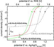
The tandem junction solar cells were measured as photocathodes in a three-electrode PEC measurement setup by means of linear sweep voltammetry measurement. From this measurement, the onset potential for cathodic current (E onset) and the photocurrent density at 0 V versus the reversible hydrogen electrode RHE (J RHE), which can be correlated with the V OC and the J SC of the solar cell, respectively, were determined for the photocathodes. In Fig. 9, the photoelectrochemical performance of the a-Si:H/µc-Si:H tandem cell with the 650 nm thin bottom cell with a 20 nm buffer layer (photocathode C in Table II, red curve) is compared to the a-Si:H/µc-Si:H reference tandem cell (photocathode A in Table II, green curve). The corresponding PV and PEC parameters are listed in Table II. The data evidences that PV and photoelectrochemical performances show the same trends: the higher the V OC and J sc of a solar cell, the higher is its E onset and J RHE as a photocathode. Still, there is a disparity in V OC and E onset values. This difference can be correlated with the overpotential for the HER. Notwithstanding this, the optimized a-Si:H/µc-Si:H tandem-based photocathode (photocathode C) showed a 100 mV increase in E onset compared to the reference tandem photocathode (photocathode A) and exhibited 1141 mV versus RHE, along with a J RHE of 9.9 mA/cm2.

FIG. 9. Linear sweep voltammetry measurements of a-Si:H/µc-Si:H with standard ZnO:Al/Ag back contact (photocathode A and C), with ZnO:Al/Ag/Pt back contact (photocathode E), and a-Si:H/a-Si:H-ZnO/Ag (photocathode F) based photocathodes in 0.1 M H2SO4 solution under 100 mW/cm2 illumination intensity at a scan rate of 30 mV s−1. Photovoltaic and photoelectrochemical parameters are listed in Table II.
TABLE II. PV (V OC, J SC) and PEC parameters (E onset, J RHE) of a-Si:H/µc-Si:H photocathodes with standard ZnO:Al/Ag back contacts (photocathode A and C, compare with Table I) and with ZnO:Al/Ag/Pt back contacts (photocathode E). Additionally, the parameters of an a-Si:H/a-Si:H photocathode are shown (photocathode F). The onset potential of cathodic current, E onset, was taken as the value at a photocurrent density of −0.5 mA/cm2 from Fig. 9.

To fully explore the performance of the photocathode, platinum was evaporated on the ZnO:Al/Ag back contact to act as a catalyst on the electrolyte side (photocathode E in Table II, gray curve). Here, no effect on J RHE is observed, proving that the optics of the photocathode back contact remain mainly unaffected by the thin platinum layer. However, with respect to the ZnO:Al/Ag back contact photocathode, the photocathode with ZnO:Al/Ag/Pt back contact shows a significant shift in E onset in positive bias direction and is measured to be 1327 mV versus RHE. This result evidences both the excellent catalytic activity of platinum as a catalyst for the HER and its viable combination with the a-Si:H/µc-Si:H/ZnO:Al/Ag tandem device.
To underline the difference between a-Si:H/µc-Si:H and a-Si:H/a-Si:H tandem junction solar cells, Fig. 9 additionally shows the linear sweep voltammetry measurement of an a-Si:H/a-Si:H based photocathode (photocathode F in Table II, dotted black curve), which will be discussed in the next section. The development and application of a-Si:H/a-Si:H photocathodes with platinum catalyst are discussed in detail in Ref. Reference Urbain, Wilken, Smirnov, Astakhov, Lambertz, Becker, Rau, Ziegler, Kaiser, Jaegermann and Finger20.
IV. DISCUSSION
Although thin film silicon-based devices, in particular a-Si:H multijunction solar cells, are among the most suitable candidates for efficient water splitting, Reference Abdi, Han, Smets, Zeman, Dam and van de Krol10,Reference Han, Abdi, Perez Rodriguez, Dam, van de Krol, Zeman and Smets12,Reference Rocheleau, Miller and Misra14 there is a tradeoff between high open-circuit voltages and high photocurrents. The presented routes of high V OC development, particularly the reduction of the intrinsic µc-Si:H absorber layer thickness, SC profiling, and buffer layer incorporation distinctly contributed to the closure of this high voltage/high current gap and considerably improved V OC in a-Si:H/µc-Si:H tandem junction solar cells, which provide significantly higher photocurrents as their all-amorphous counterparts. Thickness reduction effectively enhanced V OC. In μc-Si:H solar cells, V OC is limited by the bulk recombination in the absorber layer. Reference Pieters, Stiebig, Zeman and van Swaaij32,Reference Brammer and Stiebig33 Decreasing the thickness of this layer will therefore lead to an increase in V OC due to the reduced volume. Additionally, J SC and FF were only slightly affected, which resulted in an increased conversion efficiency for solar cells with an intrinsic µc-Si:H layer thickness of 650 nm. The highest V OC values were achieved for 450 nm thin absorber layers, but the current densities decreased, as the absorption was drastically lowered. The implementation of the SC profiling and buffer layer concept then could further increase V OC for all cell thicknesses and thus maintain conversion efficiencies above 8% for the 1300 and 650 nm thick cells and around 7% for the 450 nm thick cells. SC profiling ensures a homogeneous and moderate crystallinity level across the entire µc-Si:H absorber layer. The buffer layer at the n–i interface presumably acts as a defect passivation layer and reduces interface recombination, as already reported for heterojunction solar cells. Reference Centurioni, Iencinella, Rizzoli and Zignani34,Reference Lu, Bowden, Das and Birkmire35
The best high voltage/high current tradeoff was provided by the a-Si:H/µc-Si:H tandem cell constituted of a 650 nm thick µc-Si:H bottom cell with a 20 nm buffer layer and a 250 nm thick a-Si:H top cell (cell C in Table I), which promoted over 1.5 V and 10.0 mA/cm2 with 11.0% conversion efficiency. Furthermore, this tandem cell had a total thickness below 1 µm, accentuating its low-cost production and potential high stability against light-induced degradation. Reference Repmann, Sehrbrock, Zahren, Siekmann, Müller, Rech, Psyk, Geyer and Lechner36
Figure 10 presents the QEs for the a-Si:H/µc-Si:H tandem solar cell series (same as in Table I). By decreasing the top and the bottom cell thickness, the current densities of the top and bottom cells, J SC,top and J SC,bot, decrease while V OC increases (see Table I and Fig. 8). As the reduction of the top cell thickness is accompanied with a higher transparency, more light can enter the bottom cell. This is confirmed by the increase of the bottom cell QE in the wave length range between 400 and 600 nm with decreasing µc-Si:H absorber layer thickness (indicated by arrow in Fig. 10). This might explain the relatively high photocurrent of tandem cell B of 10.0 mA/cm2 with the 650 nm bottom cell compared to tandem cell A with the 1300 nm bottom cell, which provides 10.8 mA/cm2.

FIG. 10. Quantum efficiency measurements of the four a-Si:H/µc-Si:H tandem junction solar cells from Table I. Letter A denotes the “1300 nm” reference series (green curves), B the “1300 nm + SC profiling + buffer layer (50 nm) series” (blue curves), C the “650 nm + buffer layer (20 nm)” series (red curves), and D the “450 nm + buffer layer (5 nm)” series (black curves). The current densities of the top and bottom cells, J SC,top and J SC,bot are depicted in the figure. Letters A–D indicate tandem cells listed in Table I. Arrow indicates the trend of increasing bottom cell QE in the wave length range between 400 and 600 nm with decreasing µc-Si:H absorber layer thickness. The top and bottom cell current densities calculated from the QE-curves are placed near the related measurements. The maximum error in determination of J QE is below 0.05 mA/cm2.
The photoelectrochemical characterization revealed that PV and PEC parameters of the solar cells and photocathodes, respectively, are correlated. Short-circuit current densities J SC and J RHE are not affected, however V OC and E onset significantly differ because of overpotential losses. For the particular investigated system in this study, including the silicon photocathode with the ZnO:Al/Ag back contact and 0.1 M H2SO4 electrolyte solution, the HER overpotential was around 350 mV for all investigated photocathodes (at −0.5 mA/cm2), as can be extracted from Table II. In general, the overall performance of the tandem solar cell is reduced when applied as a photocathode in the PEC arrangement. This is mainly due to overpotential losses and mass transport limitations caused by the low conductivity of the herein used electrolyte which enforces an additional resistance on the charge transport. Reference van de Krol and Grätzel37 The related sinusoidal-like shape of the linear sweep curves (Fig. 9) is related to the reduced fill factor of the whole PEC device. In this regard, the application of different electrolyte solutions, which could reduce the electrolyte resistance, need to be tested for improving the a-Si.H/µc-Si:H photocathode performance. Nevertheless, by depositing a thin layer of platinum on the back contact, overpotential losses could be reduced by about 200 mV (Table II) and the corresponding a-Si:H/µc-Si:H photocathode exhibited an E onset of 1327 mV versus RHE. One of the most recent works focusing on the direct application of thin film silicon solar cells as photoelectrodes was done by Lin et al. Reference Lin, Battaglia, Boccard, Hettick, Yu, Ballif, Ager and Javey11 Here, single junction a-Si:H solar cells were tested as photocathodes under the irradiation by a simulated sunlight (AM 1.5 light spectrum, 100 mW/cm2) and exhibited an E onset of 0.93 V versus RHE and photocurrent densities of 6.1 mA/cm2 at 0.8 versus RHE, respectively. The a-Si:H/µc-Si:H photocathodes with Pt as a catalyst, investigated in this study, promoted a photocurrent density of 8.3 mA/cm2 at 1.0 V versus RHE, proving a significant improvement in the photocathode performance.
As already pointed out, efficient bias-free solar water splitting requires photocathodes with high photovoltages in combination with high photocurrent densities. Reference Weber and Dignam4,Reference Nozik5 Although the a-Si:H/a-Si:H photocathode, shown in Fig. 9, exhibits a high E onset over 1.56 V versus RHE, and is therefore suitable for self-contained water splitting (including overpotentials), Reference Licht, Wang, Mukerji, Soga, Umeno and Tributsch8,Reference Urbain, Wilken, Smirnov, Astakhov, Lambertz, Becker, Rau, Ziegler, Kaiser, Jaegermann and Finger20 the photocurrent density is low compared to the a-Si:H/µc-Si:H photocathodes, which limits the overall water splitting efficiency. The a-Si:H/µc-Si:H based photocathodes provide significantly higher photocurrents (Table II and indicated in Fig. 9), but the lower photovoltages only allow for small overpotential losses, and thus, for the use of precious-metal catalysts. In this regard, the hydrogen production via splitting of different acidic electrolyte solutions, like hydriodic acid (HI) or hydrobromic acid (HBr) may be advantageous for a-Si:H/µc-Si:H based PEC devices. The corresponding thermodynamic potentials for hydrogen decomposition via electrolysis are lower than 1.23 V, Reference Levy-Clement, Heller, Bonner and Parkinson38 namely 1.07 and 0.54 V for HBr and HI splitting, respectively.
V. CONCLUSION
We presented the development of a-Si:H/µc-Si:H tandem junction solar cells for the application in photoelectrochemical water splitting devices for hydrogen production. The optimization of the individual µc-Si:H single junction solar cells with focus on high open-circuit voltage, led to a 100 mV increase in V OC, while maintaining the device efficiency. The best a-Si:H/µc-Si:H tandem junction solar cell provided over 1.5 V and a conversion efficiency of 11% with a total silicon layer thickness below 1 µm.
The performance of the developed tandem junction solar cells as photocathodes was demonstrated in a PEC arrangement. In particular, the a-Si:H/µc-Si:H photocathodes with a ZnO:Al/Ag/Pt back contact exhibited a high photocurrent density of 9.9 mA/cm2 at 0 V versus RHE and an onset potential over 1.3 V versus RHE, and thus, fulfill the main thermodynamic requirement for water electrolysis. This result provides evidence that a-Si:H/µc-Si:H based PEC systems can offer a pathway toward low-cost and efficient devices for solar hydrogen generation.
Conflict of Interest
The authors declare that there is no conflict of interest regarding the publication of this paper.
Supplementary Material
To view supplementary material for this article, please visit http://dx.doi.org/jmr.2014.308.
ACKNOWLEDGMENTS
We thank K. Wilken, S. Tillmanns, L. Petter, W. Reetz, H. Siekmann, U. Gerhards, M. Hülsbeck, and A. Lambertz for their contributions to this work. The research is partly financially supported by the Deutsche Forschungsgemeinschaft (DFG) Priority Programme 1613: Regeneratively produced fuels by light driven water splitting: Investigation of involved elementary processes and perspectives of technologic implementation, and by the Bundesministerium für Bildung und Forschung (BMBF) in the network project: Sustainable Hydrogen (FKZ 03X3581B).


 Open access