Skip to main content Accessibility help
×
Hostname: page-component-8448b6f56d-sxzjt Total loading time: 0 Render date: 2024-04-18T04:21:52.941Z Has data issue: false hasContentIssue false

References

Published online by Cambridge University Press:  05 September 2013

Reza Chaji
Affiliation:
Ignis Innovation Inc., Kitchener, Ontario
Arokia Nathan
Affiliation:
University of Cambridge
Get access

Summary

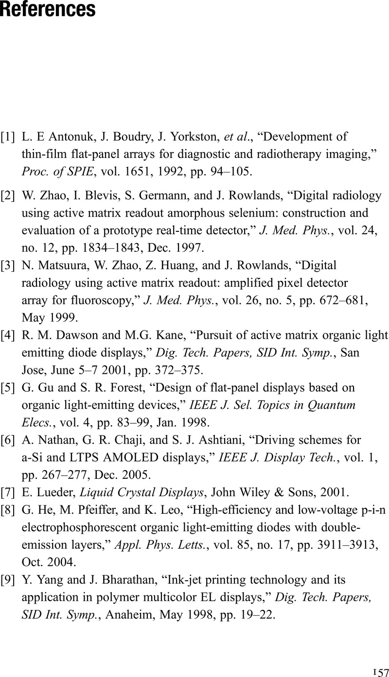
Image of the first page of this content. For PDF version, please use the ‘Save PDF’ preceeding this image.'
Type
Chapter
Information
Publisher: Cambridge University Press
Print publication year: 2013

Access options

Get access to the full version of this content by using one of the access options below. (Log in options will check for institutional or personal access. Content may require purchase if you do not have access.)

References

Antonuk, L. E, Boudry, J., Yorkston, J., et al., “Development of thin-film flat-panel arrays for diagnostic and radiotherapy imaging,” Proc. of SPIE, vol. 1651, 1992, pp. 94–105.CrossRefGoogle Scholar
Zhao, W., Blevis, I., Germann, S., and Rowlands, J., “Digital radiology using active matrix readout amorphous selenium: construction and evaluation of a prototype real-time detector,” J. Med. Phys., vol. 24, no. 12, pp. 1834–1843, Dec. 1997.CrossRefGoogle ScholarPubMed
Matsuura, N., Zhao, W., Huang, Z., and Rowlands, J., “Digital radiology using active matrix readout: amplified pixel detector array for fluoroscopy,” J. Med. Phys., vol. 26, no. 5, pp. 672–681, May 1999.CrossRefGoogle ScholarPubMed
Dawson, R. M. and Kane, M.G., “Pursuit of active matrix organic light emitting diode displays,” Dig. Tech. Papers, SID Int. Symp., San Jose, June 5–7 2001, pp. 372–375.Google Scholar
Gu, G. and Forest, S. R., “Design of flat-panel displays based on organic light-emitting devices,” IEEE J. Sel. Topics in Quantum Elecs., vol. 4, pp. 83–99, Jan. 1998.CrossRefGoogle Scholar
Nathan, A., Chaji, G. R., and Ashtiani, S. J., “Driving schemes for a-Si and LTPS AMOLED displays,” IEEE J. Display Tech., vol. 1, pp. 267–277, Dec. 2005.CrossRefGoogle Scholar
Lueder, E., Liquid Crystal Displays, John Wiley & Sons, 2001.Google Scholar
He, G., Pfeiffer, M., and Leo, K., “High-efficiency and low-voltage p-i-n electrophosphorescent organic light-emitting diodes with double-emission layers,” Appl. Phys. Letts., vol. 85, no. 17, pp. 3911–3913, Oct. 2004.CrossRefGoogle Scholar
Yang, Y. and Bharathan, J., “Ink-jet printing technology and its application in polymer multicolor EL displays,” Dig. Tech. Papers, SID Int. Symp., Anaheim, May 1998, pp. 19–22.Google Scholar
Popovic, Z. D. and Aziz, H., “Reliability and degradation of small molecule-based organic light-emitting devices (OLEDs),” IEEE J. on Sele. Topics in Quantum Elecs., vol. 8, no. 2, pp. 362–371, Mar. 2002.CrossRefGoogle Scholar
Parker, I. D., Cao, Y., and Yang, C. Y., “Lifetime and degradation effects in polymer light-emitting diodes,” J. Appl. Phys., vol. 85, no. 4, pp. 2441–2447, Feb. 1999.CrossRefGoogle Scholar
Aziz, H., Popovic, Z. D., Hu, N., Hor, A., and Xu, G., “Degradation mechanism of small molecule-based organic light-emitting devices,” Science, vol. 283, pp. 1900–1902, Mar. 1999.CrossRefGoogle ScholarPubMed
Zoua, D. and Tsutsui, T., “Voltage shift phenomena introduced by reverse-bias application in multilayer organic light emitting diodes,” J. Appl. Phys., vol. 87, no. 4, pp. 1951–1956, Feb. 2000.CrossRefGoogle Scholar
Nathan, A., Kumar, A., Sakariya, K., et al., “Amorphous silicon thin film transistor circuit integration for organic LED displays on glass and plastic,” IEEE J. Solid State Cirs., vol. 39, pp. 1477–1486, 2004.CrossRefGoogle Scholar
Mahon, J. K., “History and status of organic light-emitting device (OLED) technology for vehicular applications,” Dig. Tech. Papers, SID Int. Symp., San Jose, June 2001, pp. 22–25.Google Scholar
Lee, S. E., Oh, W. S., Lee, S. C., and Chol, J. C., “Development of a novel current controlled organic light emitting diode (OLED) display driver IC,” IEICE Tran., vol. E85, no. 11, pp. 1940–1944, Dec. 2002.Google Scholar
Ashtiani, S. J., Pixel circuits and driving schemes for active-matrix organic light-emitting diode displays, Ph.D. Thesis, University of Waterloo, 2007.
Baldo, M., The electronic and optoelectronic properties of amorphous organic semiconductors, Ph.D. Thesis, Princeton University, 2001.
Qiu, C., Peng, H., Chen, H., et al., “Top-emitting organic light-emitting diode using nanometer platinum layers as hole injector,” Dig. Tech. Papers, SID Int. Symp., Baltimore, 2003, pp. 974–977.Google Scholar
Lee, C., Moon, D., and Han, J., “Top emission organic light emitting diode with Ni anode,” Dig. Tech. Papers, SID Int. Symp., Baltimore, 2003, pp. 533–535.Google Scholar
Chang, J., Sensor system for high throughput fluorescent bio-assays, Ph.D. Thesis, University of Waterloo, 2007.
Karim, K., Pixel architectures for digital imaging using amorphous silicon technology, Ph.D. Thesis, University of Waterloo, 2007.
Izadi, M. H. and Karim, K. S., “High dynamic range pixel architecture for advanced diagnostic medical imaging applications,” J. Vac. Sci. Tech. A, vol. 24, no. 3, pp. 846–849, Feb. 2007.CrossRefGoogle Scholar
Taghibakhsh, F. and Karim, K. S., “High dynamic range 2-TFT amplifier pixel sensor architecture for digital mammography tomosynthesis,” IET Cirs. Devs. Syst., vol. 1, pp. 87–92, Feb. 2007.CrossRefGoogle Scholar
Karim, K. S., Nathan, A., Hack, M., and Milne, W. I., “Drain-bias dependence of threshold voltage stability of amorphous silicon TFTs,” IEEE Elec. Dev. Letts., vol. 25, no. 4, pp. 188–190, Apr. 2004.CrossRefGoogle Scholar
Nathan, A., Striakhilev, D., Chaji, R., et al., “Backplane requirements for active matrix organic light emitting diode displays,” Proceedings of MRS 2006, San Francisco, US, Apr. 2006, pp. 0910-A16–01-L09–01.Google Scholar
Lewis, A. G., Lee, D. D., and Bruce, R. H., “Polysilicon TFT circuit design and performance,” IEEE J. Solid State Cirs., vol. 27, pp. 1833–1842, Dec. 1992.CrossRefGoogle Scholar
Stewart, M., Howell, R., Dires, L., and Hatalis, K., “Polysilicon TFT technology for active matrix OLED displays,” IEEE Trans. on Elec. Devs., vol. 48, pp. 845–851, 2001.CrossRefGoogle Scholar
Yang, M. J., Chien, C. H., Lu, Y. H., et al., “High-performance and low-temperature-compatible p-channel polycrystalline-silicon TFTs using hafnium-silicate gate dielectric,” IEEE Elec. Dev. Letts., vol. 28, pp. 902–904, 2007.CrossRefGoogle Scholar
Servati, P., Amorphous silicon TFTs for mechanically flexible electronics, Ph.D. Thesis, University of Waterloo, 2004.
Watanabe, H., “Statistics of grain boundaries in polysilicon,” IEEE Trans. on Elec. Devs., vol. 54, pp. 38–44, Jan. 2007.CrossRefGoogle Scholar
Tai, Y. H., Huang, S. C., Chen, W. P., et al., “A statistical model for simulating the effect of LTPS TFT device variation for SOP applications,” J. Display Tech., vol. 3, pp. 426–434, Dec. 2007.Google Scholar
Street, R. A., Hydrogenated Amorphous Silicon, Cambridge University Press, 1991.CrossRefGoogle Scholar
Jackson, W. B., Marshall, M., and Moyer, M. D., “Role of hydrogen in the formation of metastable defects in hydrogenated amorphous silicon,” Phys. Rev. B, vol. 39, no. 2, pp. 1164–1179, Jan. 1989.CrossRefGoogle ScholarPubMed
Tai, Y.-H., Tsai, J.-W., Cheng, H.-C., and Su, F.-C., “Instability mechanisms for the hydrogenated amorphous silicon thin-film transistors with negative and positive bias stresses on the gate electrodes,” Appl. Phys. Letts., vol. 67, pp. 76–78, July 1995.CrossRefGoogle Scholar
Cheng, I. C. and Wagner, S., “High hole and electron field effect mobilities in nanocrystalline silicon deposited at 150 °C,” Elsevier Thin Solid Films, vol. 427, pp. 56–59, Jan. 2003.CrossRefGoogle Scholar
Esmaeili-Rad, M. R., Sazanov, A., and Nathan, A., “Absence of defect state creation in nanocrystalline silicon thin film transistors deduced from constant current stress measurements,” Appl. Phys. Letts., vol. 91, pp. 113511 (1–3), Sept. 2007.CrossRefGoogle Scholar
Esmaeili-Rad, M. R., Li, F., Sazanov, A., and Nathan, A., “Stability of nanocrystalline silicon bottom-gate thin film transistors with silicon nitride gate dielectric,” J. Appl. Phys., vol. 102, pp. 064512 (1–7), Sept. 2007.CrossRefGoogle Scholar
Lin, Y. Y., Gundlach, D. J., Nelson, S. F., and Jakson, T. N., “Stacked pentacene layer organic thin-film transistors with improved characteristics,” IEEE Elec. Dev. Letts., vol. 18, pp. 606–608, Dec. 1997.CrossRefGoogle Scholar
Li, F. M., Nathan, A., Wu, Y., and Ong, B. S., “Organic thin-film transistor integration using silicon nitride gate dielectric,” Appl. Phys. Letts., vol. 90, pp. 133514 (1–3), Mar. 2007.CrossRefGoogle Scholar
Wager, J. F., “Transparent electronics,” Science, vol. 300, pp. 1245–1246, 2003.CrossRefGoogle ScholarPubMed
Nomura, K., Ohta, H., Takagi, A., et al., “Room-temperature fabrication of transparent flexible thin-film transistors using amorphous oxide semiconductors,” Nature, vol. 432, pp. 488–492, 2004.CrossRefGoogle ScholarPubMed
Martins, R., Nathan, A., Barros, R., et al., “Complementary metal oxide semiconductor technology with and on paper, Adv. Mater., vol. 23, pp. 4491–4496, 2011.CrossRefGoogle ScholarPubMed
Nathan, A., Lee, S., Jeon, S., Song, I., Chung, U-In, “Amorphous oxide TFTs: Progress and issues,” SID Symp. Dig. Tech. Papers, vol. 43, no. 1, pp. 1–4, June 2012.CrossRefGoogle Scholar
Ghaffarzadeh, K., Nathan, A., Robertson, J., et al., “Persistent photoconductivity in Hf-In-Zn-O thin film transistors,” Appl. Phys. Letts., vol. 97, 143510 (1–3), 2010.CrossRefGoogle Scholar
Chowdhury, M. D. H., Migliorato, P., and Jang, J., “Light induced instabilities in amorphous indium–gallium–zinc–oxide thin-film transistors,” Appl. Phys. Lett., vol. 97, pp. 173506, 2010.CrossRefGoogle Scholar
Jeon, S., Ahn, S.-E., Song, I., et al., “Gated three-terminal device architecture to eliminate persistent photoconductivity in oxide semiconductor photosensor arrays,” Nature Mater., DOI: 10.1038/NMAT3256 (Feb. 2012), pp. 1–5.CrossRef
Lee, S., Ghaffarzadeh, K., Nathan, A., et al., “Trap-limited and percolation conduction mechanisms in amorphous oxide semiconductor thin film transistors,” Appl. Phys. Letts., vol. 98, pp. 203508, 2011.CrossRefGoogle Scholar
Mativenga, M., Choi, M. H., Choi, J. W., and Jang, J., “Transparent flexible circuits based on amorphous-indium–gallium–zinc–oxide thin-film transistors,” IEEE Electron Device Letts., vol. 32, p. 170, 2011.CrossRefGoogle Scholar
Martins, R., Ahnood, A., Correia, N., et al., “Recyclable, flexible, low power oxide electronics,” Adv. Funct. Mater., .
Park, J.-S., Kim, T.-W., Stryakhilev, D., et al., “Flexible full color organic light-emitting diode display on polyimide plastic substrate driven by amorphous indium gallium zinc oxide thin-film transistors,” Appl. Phys. Letts., vol. 95, pp. 013503, 2009.CrossRefGoogle Scholar
Kim, S. I., Kim, S. W., Park, J. C., et al., “Highly sensitive and reliable X-ray detector with HgI2 photoconductor and oxide drive TFT,” Tech. Dig., IEEE Electron Devices Meeting (IEDM), 2011, DOI: 10.1109/IEDM.2011.6131550, pp. 14.2.1–14.2.4.CrossRef
Jeon, S., Ahn, S. E., Song, I., et al., “Dual gate photo-thin film transistor with high photoconductive gain for high reliability, and low noise flat panel transparent imager,” Tech. Dig., IEEE Electron Devices Meeting (IEDM), 2011, DOI: 10.1109/IEDM.2011.6131551, pp. 14.3.1–14.3.4.CrossRef
Zan, H. W. and Kao, S. C., “The effect of drain-bias on the threshold voltage instability in organic TFTs,” IEEE Elec. Dev. Letts., vol. 92, pp. 155–157, Feb. 2008.CrossRefGoogle Scholar
Kim, T. H., Han, C. G., and Song, C. K., “Instability of threshold voltage under constant bias stress in pentacene thin film transistors employing polyvinylphenol gate dielectric,” Elsevier Thin Solid Films, vol. 516, pp. 1323–1326, June 2007.Google Scholar
Gu, G. and Kane, M. G., “Moisture induced electron traps and hysteresis in pentacene-based organic thin-film transistors,” Appl. Phys. Letts., vol. 92, pp. 053305 (1–3), Feb. 2008.CrossRefGoogle Scholar
Aerts, W. F., Verlaak, S., and Heremans, P., “Design of an organic pixel addressing circuit for an active-matrix OLED display,” IEEE Elec. Dev. Letts., vol. 49, pp. 2124–2126, Dec. 2002.CrossRefGoogle Scholar
Powell, M. J., Berkel, C., and Hughes, J. R., “Time and temperature dependence of instability mechanisms in amorphous silicon thin-film transistors,” J. Appl. Phys., vol. 54, pp. 1323–1325, Jan. 1989.Google Scholar
Libsch, F. R. and Kanicki, J., “Bias-stress-induced stretched-exponential time dependence of charge injection and trapping in amorphous thin-film transistors,” Appl. Phys. Letts., vol. 62, pp. 1286–1288, Mar. 1993.CrossRefGoogle Scholar
Jahinuzzaman, S. M., Sultana, A., Sakariya, K., Servati, P., and Nathan, A., “Threshold voltage instability of amorphous silicon thin-film transistors under constant current stress,” Appl. Phys. Letts., vol. 87, pp. 023502 (1–3), July 2005.CrossRefGoogle Scholar
Chiang, C. S., Kanicki, J., and Takechi, K., “Electrical instability of hydrogenated amorphous silicon thin-film transistors for active-matrix liquid-crystal displays,” Jpn. J. Appl. Phys., vol. 37, pp. 4704–4710, Sept. 1998.CrossRefGoogle Scholar
Sambandan, S., Zhu, L., Striakhilev, D., Servati, P., and Nathan, A., “Markov model for threshold-voltage shift in amorphous silicon TFTs for variable gate bias,” IEEE Elec. Dev. Letts., vol. 26, pp. 375–377, June 2005.CrossRefGoogle Scholar
He, Y., Hattori, R., and Kanicki, J., “Improved a-Si:H TFT circuits for active-matrix organic light emitting displays,” IEEE Trans. Elect. Devs., vol. 48, no. 7, pp. 1322–1325, July 2001.CrossRefGoogle Scholar
Safavian, N., Chaji, G. R., Ashtiani, S. J., Nathan, A., and Rowlands, J. A., “Self-compensated a-Si:H detector with current-mode readout circuit for digital x-ray fluoroscopy,” Proc. of IEEE MIDWEST, Cincinnati, USA, Aug. 2005.
Servati, P. and Nathan, A., “Modeling of the static and dynamic behavior of hydrogenated amorphous silicon thin-film transistors,” J. Vac. Sci. Tech., vol. 20, no. 3, pp. 1038–1042, May 2002.CrossRefGoogle Scholar
Baek, J. H., Lee, M., Lee, J. H., et al., “A current-mode display driver IC using sample-and-hold scheme for QVGA full-color active matrix organic LED mobile displays,” IEEE J. Solid State Cirs., vol. 41, no. 12, pp. 2974–2982, Dec. 2006.CrossRefGoogle Scholar
Lin, Y. C., Shieh, H. P., and Kanicki, J., “A novel current-scaling a-Si:H TFTs pixel electrode circuit for AM-OLEDs,” IEEE Trans. Elect. Devs., vol. 52, pp. 1123–1132, June 2005.CrossRefGoogle Scholar
Ono, S. and Kobayashi, Y., “An accelerative current-programming method for AM-OLED,” IEICE Trans. Elecs., vol. E88-C, pp. 264–269, Feb. 2005.CrossRefGoogle Scholar
Chaji, G. R., Ashtiani, S., Alexander, S., et al., “Pixel circuits and drive schemes for large-area a-Si AMOLED,” IDMC 2005, Taiwan, 2005.Google Scholar
Chaji, G. R. and Nathan, A., “Low-power low-cost voltage-programmed a-Si:H AMOLED display for portable devices,” IEEE J. Display Tech., vol. 4, no. 2, pp. 233–237, June 2008.CrossRefGoogle Scholar
Chaji, G. R. and Nathan, A., “Parallel addressing scheme for voltage-programmed active matrix OLED displays,” IEEE Trans. on Elec. Devs., vol. 54, pp. 1095–1100, May 2007.CrossRefGoogle Scholar
Sanford, J. L. and Libsch, F. R., “TFT AMOLED pixel circuits and driving methods,” Dig. Tech. Papers, SID Int. Symp., Baltimore, 2003, pp. 10–13.Google Scholar
Chaji, G. R., Servati, P., and Nathan, A., “Driving scheme for stable operation of 2-TFT a-Si AMOLED pixel,” IEE Electronics Letts., vol. 41, no. 8, pp. 499–500, Apr. 2005.CrossRefGoogle Scholar
Goh, J. C., Jang, J., Cho, K. S., and Kim, C. K., “A new a-Si:H thin-film transistor pixel circuit for active-matrix organic light-emitting diodes,” IEEE Elect. Dev. Letts., vol. 24, pp. 583–585, Sept. 2003.Google Scholar
Goh, J. C., Kim, C. K., and Jang, J., “A novel pixel circuit for active-matrix organic light-emitting diodes,” Dig. Tech. Paper, SID Int. Symp., Baltimore, 2003, pp. 494–497.Google Scholar
Tam, S. W., Matsueda, Y., Kimura, M., et al., “Poly-Si driving circuits for organic EL displays,” Proc. of SPIE, vol. 4295, Apr. 2001, pp. 125–133.CrossRefGoogle Scholar
Goh, J. C., Jang, J., Cho, K. S., and Kim, C. K., “A new pixel circuit for active matrix organic light emitting diodes,” IEEE Elec. Dev. Letts., vol. 23, pp. 583–585, Sept. 2002.Google Scholar
Jung, S. H., Nam, W. J., and Han, M. K, “A new voltage-modulated AMOLED pixel design compensating for threshold voltage variation in poly-Si TFTs,” IEEE Elect. Dev. Letts., vol. 25, pp. 690–692, Oct. 2004.CrossRefGoogle Scholar
Dawson, R. M. A., et al., “A polysilicon active matrix organic light emitting diode display with integrated drivers,” Dig. Tech. Papers, SID Int. Symp., 1999.
Chaji, G. R. and Nathan, A., “Stable voltage-programmed pixel circuit for AMOLED displays,” IEEE J. Display Tech., vol. 2, pp. 347–358, Dec. 2006.CrossRefGoogle Scholar
Fish, D. A., et al., “Improved optical feedback for OLED differential ageing correction,” J. SID, vol. 13, pp. 131–138, 2005.Google Scholar
Ashtiani, S. J. and Nathan, A., “A driving scheme for active-matrix organic light-emitting diode displays based on feedback,” IEEE J. Display Tech., vol. 2, pp. 258–264, Sept. 2006.CrossRefGoogle Scholar
Ashtiani, S. J. and Nathan, A., “A driving scheme for AMOLED displays based on current feedback,” Proc. of IEEE CICC, Sept. 2006, pp. 289–292.
Inukai, K., et al., “4.0-in. TFT-OLED displays and a novel digital driving scheme,” Dig. Tech. Papers, SID Int. Symp., 2000, pp. 924–927.
Kondakov, D. Y., Lenhart, W. C., and Nichols, W. F., “Operational degradation of organic light-emitting diodes: mechanism and identification of chemical products,” J. Appl. Phys., vol. 101, pp. 024512 (1–7), Jan. 2007.CrossRefGoogle Scholar
Chaji, G. R. and Nathan, A., “A novel driving scheme for high-resolution large-area a-Si:H AMOLED displays,” Proc. of IEEE MIDWEST, Cincinnati, Aug. 2005, pp. 782–785.Google Scholar
Chaji, G. R. and Nathan, A., “A sub-μA fast-settling current programmed pixel circuit for AMOLED displays,” IEEE European Solid State Cirs. (ESSCIRC 07), Sept. 2007, pp. 344–347.
Chaji, G. R., Striakhilev, D., and Nathan, A., “A novel a-Si:H AMOLED pixel circuit based on short-term stress stability of a-Si:H TFTs,” IEEE Elec. Dev. Letts., vol. 26, pp. 737–739, Oct. 2005.CrossRefGoogle Scholar
Chaji, G. R., Safavian, N., and Nathan, A., “Stable a-Si:H circuits based on short-term stability of amorphous silicon TFTs,” J. Vac. Sci. and Tech. A, vol. 24, pp. 875–878, May 2006.CrossRefGoogle Scholar
Bloom, I. and Nemirovsky, Y., “1/f noise reduction of metal-oxide-semiconductor transistors by cycling from inversion to accumulation,” Appl. Phys. Letts., vol. 58, pp. 1664–1666, Apr. 1991.CrossRefGoogle Scholar
Klumperink, E. A. M., Gerkink, J., van der Wel, A. P., and Nauta, B., “Reducing MOSFET 1/f noise and power consumption by switched biasing,” IEEE J. Solid State Cirs., vol. 35, pp. 994–1001, July 2000.CrossRefGoogle Scholar
Hassibi, A. and Lee, T. H., “A programmable electrochemical biosensor array in 0.18μm standard CMOS,” ISSCC Dig. Tech. Papers, pp. 564–566, Feb. 2005.
Hall, E. A. H., Biosensors, Open University Press, 2003.Google Scholar
Izadi, M. H. and Karim, K. S., “Noise optimization of an active pixel sensor for real-time digital x-ray fluoroscopy,” Proc. of the SPIE on Noise and Flucs. in Cir., Devices, and Materials, vol. 6600, pp. 66000Y, 2007.Google Scholar
Chaji, G. R. and Nathan, A., “A sub-μA fast-settling current programmed pixel circuit for AMOLED displays,” IEEE European Solid State Cirs. (ESSCIRC 07), Sept. 2007, pp. 344–347.
Jung, J. H., et al., “A 14.1 inch full color AMOLED display with top emission structure and a-Si backplane,” Dig. of Tech. Papers, SID Int. Symp., 2005, pp. 1538–1541.CrossRefGoogle Scholar
Wegmann, G., Vitoz, E. A., and Rahali, F., “Charge injection in analog MOS switches,” IEEE J. Solid State Cirs., vol. Sc-22, pp. 1091–1097, Dec. 1987.CrossRefGoogle Scholar
Chaji, G. R. and Nathan, A., “High-precision, fast current source for large-area current-programmed a-Si flat panels,” Proc. of IEEE ISCASS, June 2006, Greece, pp. 541–544.Google Scholar
Chaji, G. R. and Nathan, A., “Fast and offset-leakage insensitive current mode line driver for active matrix displays and sensors,” IEEE J. Display Tech., vol. 5, no. 2, pp. 72–79, Feb. 2009.CrossRefGoogle Scholar
Toumazou, C., Lidgey, F. J., and Haigh, D. G., Analogue IC Design: the Current-Mode Approach, Peter Peregrinus Ltd., 1990, pp. 93–126.Google Scholar
Sedra, A. S., Roberts, G. W., and Gohh, F., “The current conveyor: history, progress and new results,” IEE Proc. G., Elec. Cirs. Syst., vol. 137, no. 2, pp. 78–87, 1990.Google Scholar
Slotine, J. E. and Li, W., Applied Nonlinear Control, Prentice-Hall, 1991, pp. 40–99.Google Scholar
Chaji, G. R. and Nathan, A., “Low-cost stable a-Si:H AMOLED display for portable applications,” Proc. of IEEE NEWCAS, Ottawa, Canada, June 2006, pp. 97–100.Google Scholar
Chaji, G. R., Alexander, S., Nathan, A., Church, C., and Tang, S. J., “A low-cost amorphous silicon AMOLED display with full VT- and VOLED-shift compensation,” Tech. Dig. SID Symp., Long Beach, US, May 2007, pp. 1580–1583.Google Scholar
Ng, C. and Nathan, A., “Temperature characterization of a-Si:H thin-film transistor for analog circuit design using hardware description language modeling,” J. Vac. Sci. and Tech. A, vol. 24, pp. 883–887, May 2006.CrossRefGoogle Scholar
Poynton, C., Digital Video and HDTV Algorithms and Interfaces, Morgan Kaufmann Publishers, 2007.Google Scholar
Razavi, B., Design of Analog CMOS Integrated Circuits, McGraw Hill Higher Education, 2001.Google Scholar
Chaji, G. R., Safavian, N., and Nathan, A., “Dynamic-effect compensating technique for stable a-Si:H AMOLED displays,” Proc. of IEEE MIDWEST, Cincinnati, USA, Aug. 2005, pp. 786–789.Google Scholar
Safavian, N., Chaji, G. R., Nathan, A., and Rowlands, J. A., “Three-TFT image sensor for real-time digital X-ray imaging,” IEE Elec. Letts., vol. 42, no. 3, pp. 31–32, Feb. 2006.Google Scholar
Ashtiani, S. J., Servati, P., Striakhilev, D., and Nathan, A., “A 3-TFT current-programmed pixel circuit for active-matrix organic light-emitting diode displays,” IEEE Trans. Elect. Devs., vol. 52, pp. 1514–1518, July 2005.CrossRefGoogle Scholar
Johns, D. and Martin, K., Analog Integrated Circuit Design, New York, John Wiley & Sons, 1997, pp. 487–530.Google Scholar
Chaji, G. R. and Nathan, A., “A current-mode comparator for digital calibration of amorphous silicon AMOLED displays,” IEEE Trans. on Cirs. and Sys. II, vol. 55, no. 7, pp. 614–618, July 2008.Google Scholar
Chaji, G. R, Safavian, N., and Nathan, A., “Dynamic effect compensating technique for DC and transient instability of thin film transistor circuits for large-area devices,” Springer Analog Int. Cir. and Sig. Proc., vol. 56, no. 1–2, pp. 143–151, Aug. 2008.CrossRefGoogle Scholar
Chaji, G. R., Ng, C., Nathan, A., et al., “Electrical compensation of OLED luminance degradation,” IEEE Elect. Dev. Letts., vol. 28, pp. 1108–1110, Dec. 2007.CrossRefGoogle Scholar

Save book to Kindle

To save this book to your Kindle, first ensure coreplatform@cambridge.org is added to your Approved Personal Document E-mail List under your Personal Document Settings on the Manage Your Content and Devices page of your Amazon account. Then enter the ‘name’ part of your Kindle email address below. Find out more about saving to your Kindle.

Note you can select to save to either the @free.kindle.com or @kindle.com variations. ‘@free.kindle.com’ emails are free but can only be saved to your device when it is connected to wi-fi. ‘@kindle.com’ emails can be delivered even when you are not connected to wi-fi, but note that service fees apply.

Find out more about the Kindle Personal Document Service.

  • References
  • Reza Chaji, Arokia Nathan, University of Cambridge
  • Book: Thin Film Transistor Circuits and Systems
  • Online publication: 05 September 2013
  • Chapter DOI: https://doi.org/10.1017/CBO9780511998096.011
Available formats
×

Save book to Dropbox

To save content items to your account, please confirm that you agree to abide by our usage policies. If this is the first time you use this feature, you will be asked to authorise Cambridge Core to connect with your account. Find out more about saving content to Dropbox.

  • References
  • Reza Chaji, Arokia Nathan, University of Cambridge
  • Book: Thin Film Transistor Circuits and Systems
  • Online publication: 05 September 2013
  • Chapter DOI: https://doi.org/10.1017/CBO9780511998096.011
Available formats
×

Save book to Google Drive

To save content items to your account, please confirm that you agree to abide by our usage policies. If this is the first time you use this feature, you will be asked to authorise Cambridge Core to connect with your account. Find out more about saving content to Google Drive.

  • References
  • Reza Chaji, Arokia Nathan, University of Cambridge
  • Book: Thin Film Transistor Circuits and Systems
  • Online publication: 05 September 2013
  • Chapter DOI: https://doi.org/10.1017/CBO9780511998096.011
Available formats
×