Skip to main content Accessibility help
×
Hostname: page-component-8448b6f56d-dnltx Total loading time: 0 Render date: 2024-04-25T05:06:40.110Z Has data issue: false hasContentIssue false

6 - Tunnel transistors

from Section II - Tunneling devices

Published online by Cambridge University Press:  05 February 2015

Alan Seabaugh
Affiliation:
University of Notre Dame
Zhengping Jiang
Affiliation:
Purdue University
Gerhard Klimeck
Affiliation:
Purdue University
Tsu-Jae King Liu
Affiliation:
University of California, Berkeley
Kelin Kuhn
Affiliation:
Cornell University, New York
Get access

Summary

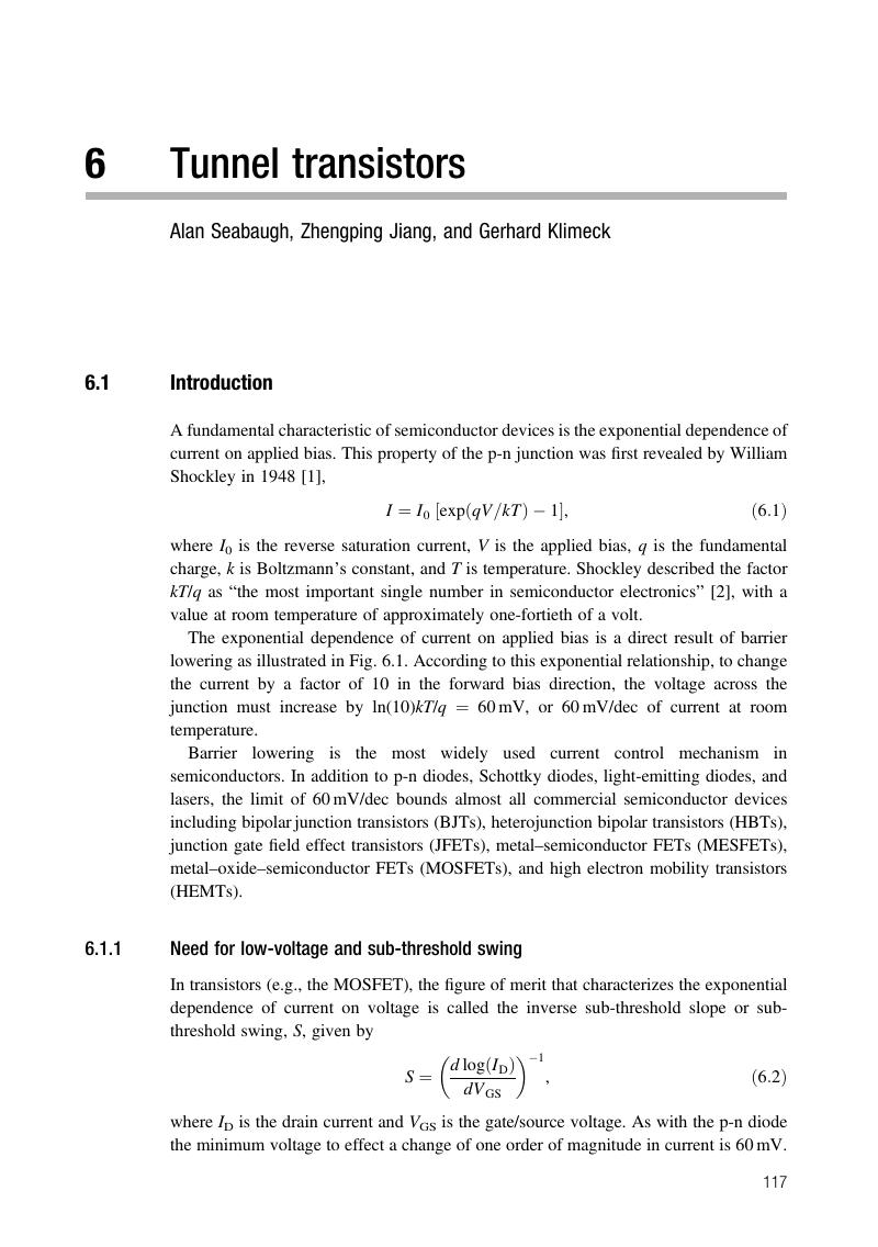
Image of the first page of this content. For PDF version, please use the ‘Save PDF’ preceeding this image.'
Type
Chapter
Information
CMOS and Beyond
Logic Switches for Terascale Integrated Circuits
, pp. 117 - 143
Publisher: Cambridge University Press
Print publication year: 2015

Access options

Get access to the full version of this content by using one of the access options below. (Log in options will check for institutional or personal access. Content may require purchase if you do not have access.)

References

Shockley, W., “The theory of p-n junctions in semiconductors and p-n junction transistors.” Bell Systems Technical Journal, 28, 439–489 (1949).CrossRefGoogle Scholar
Haynes, J. R. & Shockley, W., “Minority carriers in semiconductors.” Semiconductor Electronics Education Committee film, .
Jan, C. H., Bhattacharya, U., Brain, R. et al., “A 22nm SoC platform technology featuring 3-D tri-gate and high-k/metal gate, optimized for ultra low power, high performance and high density SoC applications.” In Electron Devices Meeting (IEDM), 2012 IEEE International, pp. 3.1.1–3.1.4 (2012).
Seabaugh, A. C. & Zhang, Q., “Low-voltage tunnel transistors for beyond CMOS logic.” Proceedings of the IEEE, 98, 2095–2110 (2010).CrossRefGoogle Scholar
Ionescu, A. M. & Riel, H., “Tunnel field-effect transistors as energy-efficient electronic switches.” Nature, 479, 329–337 (2011).CrossRefGoogle ScholarPubMed
Seabaugh, A., “The tunneling transistor.” IEEE Spectrum, 50, 35–62 (2013).CrossRefGoogle Scholar
Luisier, M. & Klimeck, G., “Simulation of nanowire tunneling transistors: From the Wentzel-Kramers-Brillouin approximation to full-band phonon-assisted tunneling.” Journal of Applied Physics, 107, 084507 (2010).CrossRefGoogle Scholar
Jena, D., “Tunneling transistors based on graphene and 2-D crystals.” Proceedings of the IEEE, 101, 1585–1602 (2013).CrossRefGoogle Scholar
Sze, S. M. & Ng, K. K., Physics of Semiconductor Devices, 3rd edn. (New York: Wiley-Interscience, 2007), p. 103.Google Scholar
Laux, S. E., “Computation of complex band structures in bulk and confined structures.” In 2009 International Workshop on Computational Electronics, pp. 1–4 (2009).
Zhang, Q., Sutar, S., Kosel, T., & Seabaugh, A., “Fully-depleted Ge interband tunnel transistor: modeling and junction formation.” Solid-State Electronics, 53, 30–35 (2009).CrossRefGoogle Scholar
Mukherjee, S., Paul, A., Neophytou, N. et al., “Band structure lab.” (2013). .
Luisier, M. & Klimeck, G., “Investigation of InxGa1-xAs ultra-thin-body tunneling FETs using a full-band and atomistic approach.” In 2009 Simulation of Semiconductor Processes and Devices (SISPAD), pp. 1–4 (2009).
Zhang, Q., Fang, T., Xing, H., Seabaugh, A., & Jena, D., “Graphene nanoribbon tunnel transistors.” IEEE Electron Device Letters, 29, 1344–1346 (2008).CrossRefGoogle Scholar
Khayer, M. A. & Lake, R. K., “Performance off n-type InSb and InAs nanowire field-effect transistors.” IEEE Transactions on Electron Devices, 55, 2939–2945 (2008).CrossRefGoogle Scholar
Zhang, Q., Lu, Y., Richter, C., Jena, D., & Seabaugh, A., “Optimum band gap and supply voltage in tunnel FETs.” IEEE Transactions on Electron Devices, 61, 2719–2724 (2014).CrossRefGoogle Scholar
NEMO5 is available under an academic open source license at: .
Steiger, S., Povolotskyi, M., Park, H.-H., Kubis, T., & Klimeck, G., “NEMO5: a parallel multiscale nanoelectronics modeling tool.” IEEE Transactions on Nanotechnology, 10, 1464 (2011).CrossRefGoogle Scholar
Klimeck, G., Bowen, R., Boykin, T., & Cwik, T., “sp3s* tight-binding parameters for transport simulations in compound semiconductors.” Superlattices and Microstructures, 27, 519–524 (2000).CrossRefGoogle Scholar
Boykin, T., Klimeck, G., Bowen, R., & Oyafuso, F., “Diagonal parameter shifts due to nearest-neighbor displacements in empirical tight-binding theory.” Physics Reviews B, 66, 125207 (2002).CrossRefGoogle Scholar
Klimeck, G., Oyafuso, F., Boykin, T., Bowen, R., & Allmen, P., “Development of a nanoelectronic 3-D (NEMO 3-D) simulator for multimillion atom simulations and its application to alloyed quantum dots.” Computer Modeling in Engineering and Science (CMES), 3(5), 601–642 (2002).Google Scholar
Smith, D. L. & Maihiot, C., “Proposal for strained type II superlattice infrared detectors.” Journal of Applied Physics, 62, 2545 (1987).CrossRefGoogle Scholar
Sai-Halasz, G. A., Tsu, R., & Esaki, L., “A new semiconductor superlattice.” Applied Physics Letters 30, 651 (1977).CrossRefGoogle Scholar
Luisier, M. & Klimeck, G., “Performance comparisons of tunneling field-effect transistors made of InSb, carbon, and GaSb-InAs broken gap heterostructures.” In Electron Devices Meeting (IEDM), 2009 IEEE International, pp. 37.6.1–37.6.4 (2009).
Koswatta, S. O., Koester, S. J., & Haensch, W., “On the possibility of obtaining MOSFET-like performance and sub-60-mV/dec swing in 1-D broken-gap tunnel transistors.” IEEE Transactions on Electron Devices, 57, 3222–3230 (2010).CrossRefGoogle Scholar
Luisier, M. & Klimeck, G., “Atomistic, full-band design study of InAs band-to-band tunneling field-effect transistors.” IEEE Electron Device Letters, 30, 602–604 (2009).CrossRefGoogle Scholar
Hu, C., Chou, D., Patel, P., & Bowonder, A., “Green transistor – a VDD scaling path for future low power ICs.” In VLSI Technology, Systems and Applications, 2008. VLSI-TSA 2008. International Symposium on, pp. 14–15 (2008).
Agarwal, S., Klimeck, G., & Luisier, M., “Leakage reduction design concepts for low power vertical tunneling field-effect transistors.” IEEE Electronic Device Letters, 31, 621–623 (2010).CrossRefGoogle Scholar
Luisier, M., Agarwal, S., & Klimeck, G., “Tunneling field-effect transistor with low leakage current.” US Patent No. 8,309,989, November 13 (2012).
Lu, Y., Zhou, G., Li, R. et al., “Performance of AlGaSb/InAs TFETs with gate electric field and tunneling direction aligned.” IEEE Electron Device Letters, 33, 655–657 (2012).CrossRefGoogle Scholar
Knoch, J. & Appenzeller, J., “Modeling of high-performance p-Type III-V heterojunction tunnel FETs.” IEEE Electron Device Letters, 31, 305–307, (2010).CrossRefGoogle Scholar
Avci, U. E., Rios, R., Kuhn, K. J., & Young, I. A., “Comparison of power and performance for the TFET and MOSFET and considerations for P-TFET.” In Nanotechnology (IEEE-NANO), 2011 IEEE Conference on, pp. 869–872 (2011).
Nanavati, R. P. & De Andrade, C. A. M., “Excess current in gallium arsenide tunnel diodes.” Proceedings of the IEEE, 52, 869–870 (1964).CrossRefGoogle Scholar
Nanavati, R. P. & Eisencraft, M., “On thermal and excess currents in GaSb tunnel diodes.” IEEE Transactions on Electron Devices, 15, 796–797 (1968).CrossRefGoogle Scholar
Seabaugh, A. & Lake, R., “Tunnel diodes.” In Encyclopedia of Applied Physics, vol. 22 (New York: Wiley, 1998), pp. 335–359.Google Scholar
Bessire, C. D., Björk, M. T., Schmid, H., Schenk, A., Reuter, K. B., & Riel, H., “Trap-assisted tunneling in Si-InAs nanowire heterojunction tunnel diodes.” Nano Letters, 11, 4195–4199 (2011).CrossRefGoogle ScholarPubMed
Steiger, S., Veprek, R. G., & Witzigmann, B., “Electroluminescence from a quantum-well LED using NEGF.” In 2009 International Workshop on Computational Electronics, (IWCE), pp. 1–4 (2009).
Pala, M. G. & Esseni, D., “Interface traps in InAs nanowire tunnel-FETs and MOSFETs – part I: model description and single trap analysis in tunnel-FETs.” IEEE Transactions on Electron Devices, 60, 2795–2801 (2013).CrossRefGoogle Scholar
Esseni, D. & Pala, M. G., “Interface traps in InAs nanowire tunnel FETs and MOSFETs – part II: comparative analysis and trap-induced variability.” IEEE Transactions on Electron Devices, 60, 2802–2807 (2013).CrossRefGoogle Scholar
Cohen, M. H., Chou, M. Y., Economou, E. N., John, S., & Soukoulis, C. M., “Band tails, path integrals, instantons, polarons, and all that.” IBM Journal of Research and Development, 32, 82–92 (1988).CrossRefGoogle Scholar
Cho, W.-S., Luisier, M., Mohata, D. et al., “Full band modeling of homo-junction InGaAs band-to-band tunneling diodes including band gap narrowing.” Applied Physics Letters, 100, 063504 (2012).CrossRefGoogle Scholar
Lake, R., Klimeck, G., Bowen, R., & Jovanovic, D., “Single and multiband modeling of quantum electron transport through layered semiconductor devices.” Journal of Applied Physics, 81, 7845–7869 (1997).CrossRefGoogle Scholar
Rivas, C., Lake, R., Klimeck, G. et al., “Full band simulation of indirect phonon-assisted tunneling in a silicon tunnel diode with delta-doped contacts.” Applied Physics Letters, 78, 814–816 (2001).CrossRefGoogle Scholar
Luisier, M. & Klimeck, G., “Atomistic full-band simulations of Si nanowire transistors: effects of electron-phonon scattering.” Physics Reviews B, 80, 155430 (2009).CrossRefGoogle Scholar
Khayer, M. A. and Lake, R. K., “Effects of band-tails on the subthreshold characteristics of nanowire band-to-band tunneling transistors.” Journal of Applied Physics, 110, 074508 (2011).CrossRefGoogle Scholar
Luisier, M. & Klimeck, G., “Performance analysis of statistical samples of graphene nanoribbon tunneling transistors with line edge roughness.” Applied Physics Letters, 94, 223505 (2009).CrossRefGoogle Scholar
Klimeck, G., Lake, R., & Blanks, D., “Numerical approximations to the treatment of interface roughness scattering in resonant tunneling diodes.” Semiconductor Science and Technology, 13, A165 (1998).CrossRefGoogle Scholar
Takagi, S., Toriumi, A., Iwase, M., & Tango, H., “On the universality of inversion layer mobility in Si MOSFET’s: Part II – effects of surface orientation.” IEEE Transactions on Electron Devices, 41, 2363–2368 (1994).CrossRefGoogle Scholar
Jin, S., Fischetti, M. V., & Tang, T.-W., “Modeling of electron mobility in gated silicon nanowires at room temperature: surface roughness scattering, dielectric screening, and band nonparabolicity.” Journal of Applied Physics, 102, 083715 (2007).CrossRefGoogle Scholar
Kim, S. G., Paul, A., Luisier, M., Boykin, T., & Klimeck, G., “Full three-dimensional quantum transport simulation of atomistic interface roughness in silicon nanowire FETs.” IEEE Transactions on Electron Devices, 58, 1371–1380 (2011).Google Scholar
Conzatti, F., Pala, M. G., & Esseni, D., “Surface-roughness-induced variability in nanowire InAs tunnel FETs.” IEEE Electron Device Letters, 33, 806–808 (2012).CrossRefGoogle Scholar
Li, R., Lu, Y., Zhou, G. et al., “AlGaSb/InAs tunnel field-effect transistor with on-current of 78 μA/μm at 0.5 V.” IEEE Electron Device Letters, 33, 363–365 (2012).CrossRefGoogle Scholar
Boykin, T., Kharche, N., & Klimeck, G., “Brillouin-zone unfolding of perfect supercells having nonequivalent primitive cells illustrated with a Si/Ge tight-binding parameterization.” Physics Reviews B 76, 035310 (2007).CrossRefGoogle Scholar
Boykin, T., Kharche, N., Klimeck, G., & Korkusinski, M., “Approximate bandstructures of semiconductor alloys from tight-binding supercell calculations.” Journal of Physics: Condensed Matter, 19, 036203 (2007).Google Scholar
Oyafuso, F., Klimeck, G., Bowen, R., & Boykin, T., “Atomistic electronic structure calculations of unstrained alloyed systems consisting of a million atoms.” Journal of Computational Electronics, 1, 317–321 (2002).CrossRefGoogle Scholar
Oyafuso, F., Klimeck, G., Bowen, R., Boykin, T., & Allmen, P., “Disorder induced broadening in multimillion atom alloyed quantum dot systems.” Physica Status Solidi (C), 0, 1149–1152 (2003).CrossRefGoogle Scholar
Kharche, N., Prada, M., Boykin, T., & Klimeck, G., “Valley-splitting in strained silicon quantum wells modeled with 2 miscuts, step disorder, and alloy disorder.” Applied Physics Letters 90, 092109 (2007).CrossRefGoogle Scholar
Boykin, T., Luisier, M., Schenk, A., Kharche, N., & Klimeck, G., “The electronic structure and transmission characteristics of AlGaAs nanowires.” IEEE Transactions on Nanotechnology, 6, 43–47 (2007).CrossRefGoogle Scholar
Avci, U. E., Rios, R., Kuhn, K., & Young, I. A., “6B-5 comparison of performance, switching energy and process variations for the TFET and MOSFET in logic.” In VLSI Technology (VLSIT), 2011 Symposium on, pp. 124–125 (2011).
Avci, U. E., Morris, D. H., Hasan, S., & Kotlyar, R., “Energy efficiency comparison of nanowire heterojunction TFET and Si MOSFET at Lg = 13 nm, including P-TFET and variation considerations.” In Electron Devices Meeting (IEDM), 2013 IEEE International, pp. 33.4.1–33.4.4 (2013).
Mookerjea, S., Mohata, D., Krishnan, R. et al., “Experimental demonstration of 100nm channel length In0.53Ga0.47As-based vertical inter-band tunnel field effect transistors (TFETs) for ultra low-power logic and SRAM applications.” In Electron Devices Meeting (IEDM), 2009 IEEE International, pp. 13.7.1–13.7.3 (2009).
Mookerjea, S., Mohata, D., Mayer, T., Narayanan, V., & Datta, S., “Temperature-dependent I–V characteristics of a vertical In0.53Ga0.47As tunnel FET.” IEEE Electron Device Letters, 31, 564–566, (2010).CrossRefGoogle Scholar
Zhao, H., Chen, Y., Wang, Y., Zhou, F., Xue, F., & Lee, J., “In0.7Ga0.3As tunneling field-effect transistors with an Ion of 50 μA/μm and a subthreshold swing of 86 mV/dec using HfO2 gate oxide.” IEEE Electron Devices Letters, 31, 1392–1394 (2010).CrossRefGoogle Scholar
Zhao, H., Chen, Y., Wang, Y., Zhou, F., Xue, F., and Lee, J., “InGaAs tunneling field-effect-transistors with atomic-layer-deposited gate oxides.” IEEE Transactions on Electron Devices, 58, 2990–2995 (2011).CrossRefGoogle Scholar
Mohata, D. K., Bijesh, R., Mujumdar, S. et al., “Demonstration of MOSFET-like on-current performance in arsenide/antimonide tunnel FETs with staggered hetero-junctions for 300 mV logic applications.” In Electron Devices Meeting (IEDM), 2011 IEEE International, pp. 33.5.1–4 (2011).
Mohata, D. K., Bijesh, R., Saripalli, V., Mayer, T., & Datta, S., “Self-aligned gate nanopillar In0.53Ga0.47As vertical tunnel transistor.” In 2011 Device Research Conference (DRC), pp. 203–204 (2011).
Mohata, D., Mookerjea, S., Agrawal, A. et al., “Experimental staggered-source and n+ pocket-doped channel III-V tunnel field-effect transistors and their scalabilities.” Applied Physics Express, 4, 024105 (2011).CrossRefGoogle Scholar
Mohata, D., Rajamohanan, B., Mayer, T. et al., “Barrier-engineered arsenide–antimonide heterojunction tunnel FETs with enhanced drive current.” IEEE Electron Device Letters, 33, 1568–1570 (2012).CrossRefGoogle Scholar
Ford, A. C., Yeung, C. W., Chuang, S. et al., “Ultrathin body InAs tunneling field-effect transistors on Si substrates.” Applied Physics Letters, 98, 113105 (2011).CrossRefGoogle Scholar
Li, R., Lu, Y., Chae, S. D. et al., “InAs/AlGaSb heterojunction tunnel field-effect transistor with tunnelling in-line with the gate field.” Physica Status Solidi (C), 9, 389–392 (2011).CrossRefGoogle Scholar
Li, R., Lu, Y., Zhou, G. et al., “InAs/AlGaSb heterojunction tunnel FET with InAs airbridge drain.” In Compound Semiconductors (ISCS), 2011 International Symposium on, pp. 189–190 (2011).
Zhou, G., Lu, Y., Li, R. et al., “Self-aligned In0.53Ga0.47As/InP vertical tunnel FET.” In Compound Semiconductor Manufacturing Technology (CS ManTech), 2011 International Conference on, (2011).
Zhou, G., Lu, Y., Li, R. et al., “Vertical InGaAs/InP tunnel FETs with tunneling normal to the gate.” IEEE Electron Devices Letters, 32, 1516–1518 (2011).CrossRefGoogle Scholar
Zhou, G., Lu, Y., Li, R. et al., “InGaAs/InP tunnel FETs with a subthreshold swing of 93 mV/dec and Ion/Ioff ratio near 106.” IEEE Electron Devices Letters, 33, 782–84 (2012).CrossRefGoogle Scholar
Zhou, G., Lu, Y., Li, R. et al., “Self-aligned InAs/Al0.45Ga0.55Sb vertical tunnel FETs.” In Device Research Conference (DRC), 2011 69th Annual, pp. 205–206 (2011).
Zhou, G., Li, R., Vasen, T. et al., “Novel gate-recessed vertical InAs/GaSb TFETs with record high Ion of 180 μA/μm at VDS = 0.5 V.” In Electron Devices Meeting (IEDM), 2012 IEEE International, pp. 32.6.1–32.6.4 (2012).
Dey, A. W., Borg, B. M., Ganjipour, B. et al., “High current density InAsSb/GaSb tunnel field effect transistors.” In Devices Research Conference (DRC), 2012 IEEE, pp. 205–206 (2012).
Dey, A. W., Borg, B. M., Ganjipour, B. et al., “High-current GaSb/InAs(Sb) nanowire tunnel field-effect transistors.” IEEE Electron Device Letters, 34, 211–213 (2013).CrossRefGoogle Scholar
Bijesh, R., Liu, H., Madan, H. et al., “Demonstration of In0.9Ga0.1As/GaAs0.18Sb0.82 near broken-gap tunnel FET with Ion = 740 μA/μm, GM = 700 μS/μm and gigahertz switching performance at VDS = 0.5V.” In Electron Devices Meeting (IEDM), 2013 IEEE International, pp. 28.2.1–28.2.4 (2013).
Dewey, G., Chu-Kung, B., Boardman, J. et al., “Fabrication, characterization, and physics of III-V heterojunction tunneling field effect transistors (H-TFET) for steep sub-threshold swing.” Electron Devices Meeting (IEDM), 2011 IEEE International, pp. 33.6.1–33.6.4 (2011).
Dewey, G., Chu-Kung, B., Kotlyar, R., Metz, M., Mukherjee, N., & Radosavljevic, M., “III-V field effect transistors for future ultra-low power applications.” In VLSI Technology (VLSIT), 2012 Symposium on, pp. 45–46 (2012).
Avci, U. E., Hasan, S., Nikonov, D. E., Rios, R., Kuhn, K., & Young, I. A., “Understanding the feasibility of scaled III-V TFET for logic by bridging atomistic simulations and experimental results.” In VLSI Technology (VLSIT), 2012 Symposium on, pp. 183–184 (2012).
Tomioka, K., Yoshimura, M., & Fukui, T., “Steep-slope tunnel field-effect transistors using III-V nanowire/Si heterojunction.” In VLSI Technology (VLSIT), 2012 Symposium on, pp. 47–48 (2012).
Noguchi, M., Kim, S., Yokoyama, M. et al., “High Ion/Ioff and low subthreshold slope planar-type InGaAs tunnel FETs with Zn-diffused source junctions.” In Electron Devices Meeting (IEDM), 2013 IEEE International, pp. 28.1.1–4 (2013).
Borg, B. M., Dick, K. A., Ganjipour, B., Pistol, M.-E., Wernersson, L.-E., & Thelander, C., “InAs/GaSb heterostructure nanowires for tunnel field-effect transistors.” Nano Letters, 10, 4080–4085 (2010).CrossRefGoogle ScholarPubMed
Tomioka, K. & Fukui, T., “Tunnel field-effect transistor using InAs nanowire/Si heterojunction.” Applied Physics Letters, 98, 083114 (2011).CrossRefGoogle Scholar
Moselund, K. E., Schmid, H., Bessire, C., Bjork, M. T., Ghoneim, H., & Riel, H., “InAs–Si nanowire heterojunction tunnel FETs.” IEEE Electron Device Letters, 33, 1453–1455 (2012).CrossRefGoogle Scholar
Riel, H., Moselund, K. E., Bessire, C. et al., “InAs-Si heterojunction nanowire tunnel diodes and tunnel FETs.” In Electron Devices Meeting (IEDM), 2012 IEEE International, pp. 16.6.1–16.6.4 (2012).
Borg, B. Mattias, Ek, M., Dick, K. A. et al., “Diameter reduction of nanowire tunnel heterojunctions using in situ annealing.” Applied Physics Letters, 99, 203101 (2011).CrossRefGoogle Scholar
Rajamohanan, B., Mohata, D., Zhernokletov, D. et al., “Low-temperature atomic-layer-deposited high-κ dielectric for p-channel In0.7Ga0.3As/GaAs0.35Sb0.65 heterojunction tunneling field-effect transistor.” Applied Physics Express, 6, 101201 (2013).CrossRefGoogle Scholar
Lu, H. & Seabaugh, A., “Tunnel field-effect transistor: state-of-the-art.” IEEE Journal of the Electron Devices Society, 2, 44–49 (2014).CrossRefGoogle Scholar

Save book to Kindle

To save this book to your Kindle, first ensure coreplatform@cambridge.org is added to your Approved Personal Document E-mail List under your Personal Document Settings on the Manage Your Content and Devices page of your Amazon account. Then enter the ‘name’ part of your Kindle email address below. Find out more about saving to your Kindle.

Note you can select to save to either the @free.kindle.com or @kindle.com variations. ‘@free.kindle.com’ emails are free but can only be saved to your device when it is connected to wi-fi. ‘@kindle.com’ emails can be delivered even when you are not connected to wi-fi, but note that service fees apply.

Find out more about the Kindle Personal Document Service.

Available formats
×

Save book to Dropbox

To save content items to your account, please confirm that you agree to abide by our usage policies. If this is the first time you use this feature, you will be asked to authorise Cambridge Core to connect with your account. Find out more about saving content to Dropbox.

Available formats
×

Save book to Google Drive

To save content items to your account, please confirm that you agree to abide by our usage policies. If this is the first time you use this feature, you will be asked to authorise Cambridge Core to connect with your account. Find out more about saving content to Google Drive.

Available formats
×