Skip to main content Accessibility help
×
Hostname: page-component-76fb5796d-9pm4c Total loading time: 0 Render date: 2024-04-25T16:01:42.515Z Has data issue: false hasContentIssue false

10 - The piezoelectronic transistor

from Section III - Alternative field effect devices

Published online by Cambridge University Press:  05 February 2015

Paul M. Solomon
Affiliation:
IBM
Bruce G. Elmegreen
Affiliation:
IBM
Matt Copel
Affiliation:
IBM
Marcelo A. Kuroda
Affiliation:
IBM
Susan Trolier-McKinstry
Affiliation:
Pennsylvania State University
Glenn J. Martyna
Affiliation:
IBM
Dennis M. Newns
Affiliation:
IBM
Tsu-Jae King Liu
Affiliation:
University of California, Berkeley
Kelin Kuhn
Affiliation:
Cornell University, New York
Get access

Summary

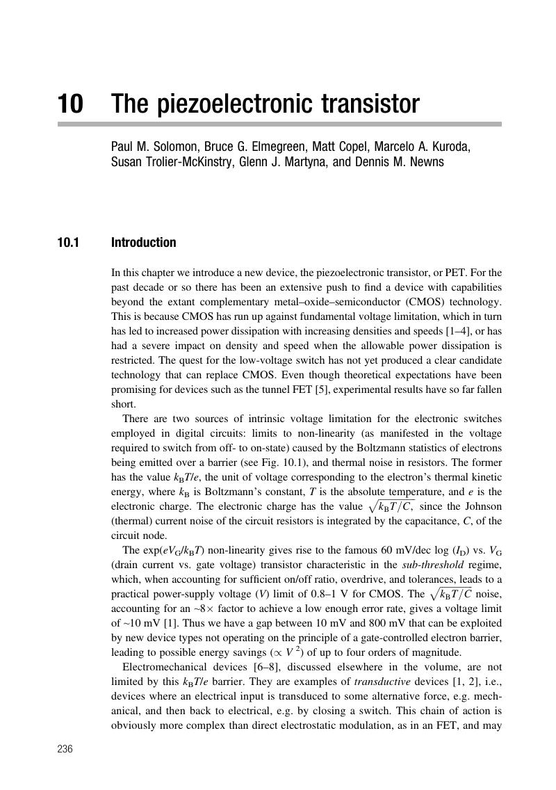
Image of the first page of this content. For PDF version, please use the ‘Save PDF’ preceeding this image.'
Type
Chapter
Information
CMOS and Beyond
Logic Switches for Terascale Integrated Circuits
, pp. 236 - 262
Publisher: Cambridge University Press
Print publication year: 2015

Access options

Get access to the full version of this content by using one of the access options below. (Log in options will check for institutional or personal access. Content may require purchase if you do not have access.)

References

Theis, T. N. & Solomon, P. M., “In quest of the ‘next switch’: prospects for greatly reduced power dissipation in a successor to the silicon field effect transistor.” Proceedings of the IEEE, 87(12), 2005–2014 (2010).CrossRefGoogle Scholar
Theis, T. N., “In quest of a fast, low-voltage digital switch.” ECS Transactions, 45(6), 3–11 (2012).CrossRefGoogle Scholar
Haensch, W., Nowak, E. J., Dennard, R. H., & Solomon, P. M. et al., “Silicon CMOS devices beyond scaling.” IBM Journal of Research and Development, 50(4/5), 339–358 (2006).CrossRefGoogle Scholar
Iwai, H., “Roadmap for 22 nm and beyond.” Microelectronic Engineering, 86, 1520–1528 (2009).CrossRefGoogle Scholar
Seabaugh, A. C., “Low-voltage tunnel transistors for beyond CMOS logic.” Proceedings of the IEEE, 98(12), 2095–2110 (2010).CrossRefGoogle Scholar
Feng, X. L., Matheny, M. H., Zorman, C. A., Mehregany, M., & Roukes, M. L., “Low voltage nanoelectromechanical switches based on silicon carbide nanowires.” Nano Letters, 10(8), 2891–2896 (2010).CrossRefGoogle ScholarPubMed
Akarvardar, K. & Wong, H.-S., “Nanoelectromechanical logic and memory devices.” ECS Transactions 19(1), 49–59 (2009).CrossRefGoogle Scholar
Liu, T.-J. K., Alon, E., Stojanovic, V., & Markovic, D., “The relay reborn.” IEEE Spectrum, April (2012).
Newns, D., Elmegreen, B., Liu, X.-H., & Martyna, G., “A low-voltage high-speed electronic switch based on piezoelectric transduction.” Journal of Applied Physics, 111, 084509, (2012).CrossRefGoogle Scholar
Newns, D. M., Elmegreen, B. G., Liu, X.-H., & Martyna, G. J., “The piezoelectronic transistor: a nanoactuator-based post-CMOS digital switch with high speed and low power.” MRS Bulletin, 37, 1071–1076 (2012).CrossRefGoogle Scholar
Newns, D. M., Elmegreen, B. G., Liu, X.-H., & Martyna, G. J., “High response piezoelectric and piezoresistive materials for fast, low voltage switching: simulation and theory of transduction physics at the nanometer-scale.” Advanced Materials, 24(27), 3672–3677 (2012).CrossRefGoogle ScholarPubMed
Jayaraman, A., Narayanamurti, V., Bucher, E., & Maines, R. G., “Continuous and discontinuous semiconductor-metal transition in samarium monochalcogenides under pressure.” Physics Review Letters, 25(20), 1430–1433 (1970).CrossRefGoogle Scholar
Helnwein, P., “Some remarks on the compressed matrix representation of symmetric second-order and fourth-order tensors.” Computer Methods in Applied Mechanics and Engineering, 190(22–23), 2753–2770 (2001).CrossRefGoogle Scholar
Zhang, S. & Li, F., “High performance ferroelectric relaxor-PbTiO3 single crystals: Status and perspective.” Journal of Applied Physics, 111, 031301 (2012).Google Scholar
Fu, H. & Cohen, R. E., “Polarization rotation mechanism for ultrahigh electromechanical response in single-crystal piezoelectrics.” Nature, 403, 281–283 (2000).CrossRefGoogle ScholarPubMed
Bai, F., Li, J., & Viehland, D., “Domain engineered states over various length scales in (001)-oriented Pb(Mg1/3Nb2/3)O 3 -x%PbTiO3 crystals: electrical history dependence of hierarchal domains.” Journal of Applied Physics, 97(5), 054103 (2005).CrossRefGoogle Scholar
Shuvaeva, V. A., Glazer, A. M., & Zekria, D., “The macroscopic symmetry of Pb(Mg1/3Nb2/3)1−xTiO3 in the morphotropic phase boundary region (x = 0.25–0.5).” Journal of Physics: Condensed Matter, 17, 5709–5723 (2005).Google Scholar
Mc Whan, D. B. & Remelka, J. B., “Metal-insulator transition in metaloxides.” Physics Reviews B, 2(9), 3734–3750 (1970).CrossRefGoogle Scholar
Jayaraman, A., Narayanamurti, V., Bucher, E., & Maines, R. G., “Pressure-induced metal-semiconductor transition and 4f electron delocalization in SmTe.” Physics Review Letters, 25(6), 368–370 (1970).CrossRefGoogle Scholar
Jayaraman, A. & Maines, R. G., “Study of valence transitions in Eu-, Yb-, and Ca-substituted SmS under high pressure and some comments on other substitutions.” Physics Reviews B, 19(8), 4154–4161 (1979).CrossRefGoogle Scholar
Jayaraman, A., Singh, A. K., Chatterjee, A., & Devi, S. U., “Pressure-volume relationship and pressure-induced electronic and structural transformations in Ku and Yb monochalcogenides.” Physics Reviews B, 9(6), 2513–2520 (1974).CrossRefGoogle Scholar
Jiang, Z., Kuroda, M. A., Tan, Y. et al., “Electron transport in nano-scaled piezoelectronic devices.” Applied Physics Letters, 102(19), 193501 (2013).CrossRefGoogle Scholar
Gupta, D. C. & Kulshrestha, S., “Pressure induced magnetic, electronic and mechanical properties of SmX (X = Se, Te).” Journal of Physics: Condensed Matter, 21, 436011 (2009).Google Scholar
Tiersten, H. F., Linear Piezoelectric Plate Vibrations; Elements of the Linear Theory of Piezoelectricity and the Vibrations of Piezoelectric Plates (New York: Springer, 1995).Google Scholar
Close, C. M., Frederick, D. K., & Newell, J. C., Modeling and Analysis of Dynamic Systems, 3rd edn. (Chichester: Wiley, 2001).Google Scholar
Terman, F. E., Radio Engineers Handbook (New York: McGraw Hill, 1943).Google Scholar
Copel, M., Kuroda, M. A., Gordon, M. S., & Liu, X.-H. et al. “Giant piezoresistive on/off ratios in rare-earth chalcogenide thin films enabling nanomechanical switching.” Nano Letters, 13(10), 4650–4653 (2013).CrossRefGoogle ScholarPubMed
Park, J. H., Xu, F., & Trolier-McKinstry, S., “Dielectric and piezoelectric properties of sol–gel derived lead magnesium niobium titanate films with different textures.” Journal of Applied Physics, 89(1), 568–574 (2001).CrossRefGoogle Scholar
Keech, R., Shetty, S., & Kuroda, M. A., “Lateral scaling of Pb(Mg1/3Nb2/3)O3−PbTiO3 thin films for piezoelectric logic applications.” Journal of Applied Physics, 115, 234106 (2014).CrossRefGoogle Scholar
Nikonov, D. E. & Young, I. A., “Uniform methodology for benchmarking beyond-CMOS logic devices.” In Electron Devices Meeting (IEDM), 2012 IEEE International), pp. 10–13 (2012).
Franklin, A. D., Luisier, M., Han, S-J. et al., “Sub-10 nm carbon nanotube transistor.” Nano Letters, 12(2), 758–762 (2012).CrossRefGoogle ScholarPubMed
Franklin, A. D., Koswatta, S. O., Farmer, D. B. et al., “Carbon nanotube complementary wrap-gate transistors.” Nano Letters, 13(6), 2490−2495 (2013).CrossRefGoogle ScholarPubMed
Solomon, P. M., Frank, D. J., & Koswatta, S. O., “Compact model and performance estimation for tunneling nanowire FET.” In Proceedings of the 69th Annual Device Research Conference, pp. 197–198 (2011).
Podzorov, V., Gershenson, M. E., Kloc, Ch., Zeis, R., & Bucher, E.High mobility field-effect transistors based on transition metal dichalcogenides.” Applied Physics Letters, 84(17), 3301–3303 (2004).CrossRefGoogle Scholar
Banerjee, S. K., Register, L. F., Tutuc, E., Reddy, D., & MacDonald, A. H., “Bilayer pseudo-spin field-effect transistor (BiSFET): a proposed new logic device.” IEEE Electron. Devices Letters, 30(2), 158–60 (2009).CrossRefGoogle Scholar

Save book to Kindle

To save this book to your Kindle, first ensure coreplatform@cambridge.org is added to your Approved Personal Document E-mail List under your Personal Document Settings on the Manage Your Content and Devices page of your Amazon account. Then enter the ‘name’ part of your Kindle email address below. Find out more about saving to your Kindle.

Note you can select to save to either the @free.kindle.com or @kindle.com variations. ‘@free.kindle.com’ emails are free but can only be saved to your device when it is connected to wi-fi. ‘@kindle.com’ emails can be delivered even when you are not connected to wi-fi, but note that service fees apply.

Find out more about the Kindle Personal Document Service.

Available formats
×

Save book to Dropbox

To save content items to your account, please confirm that you agree to abide by our usage policies. If this is the first time you use this feature, you will be asked to authorise Cambridge Core to connect with your account. Find out more about saving content to Dropbox.

Available formats
×

Save book to Google Drive

To save content items to your account, please confirm that you agree to abide by our usage policies. If this is the first time you use this feature, you will be asked to authorise Cambridge Core to connect with your account. Find out more about saving content to Google Drive.

Available formats
×