Introduction
Gallium Nitride (GaN) has become an important material for ultraviolet light emitters and detectors, as well as high power, high frequency electronic devices. It has been demonstrated that growth of GaN on sapphire by lateral epitaxial overgrowth (LEO) [Reference Nakamura, Senoh, Nagahama, Iwasa, Yamada, Matsushita, Sugimoto, Kozaki, Umemoto, Sano and Chocho1-Reference Sasaoka, Sunakawa, Kimura, Nido, Usui and Sakai3] greatly reduces the threading dislocation density in this material. A device lifetime of more than 10000 h at room temperature has been reported for cw operation of InGaN multiple quantum well laser diodes employing LEO GaN grown by metalorganic chemical vapor deposition (MOCVD) [Reference Nakamura, Senoh, Nagahama, Iwasa, Yamada, Matsushita, Sugimoto, Kozaki, Umemoto, Sano and Chocho1], and a significant decrease of p-n junction reverse leakage current in LEO materials has also been observed [Reference Sasaoka, Sunakawa, Kimura, Nido, Usui and Sakai3]. However, little is known about the room temperature dynamics of resonantly created excitons and free carriers with low excess energy crucial to an understanding of device performance in this high quality GaN.
In this paper we present a time-resolved pump-probe study of exciton and free carrier dynamics in LEO GaN in which photoinduced changes in reflectivity ΔR are monitored on a picosecond timescale. The ΔR transients were obtained as a function of excitation intensity for three cases: (i) resonantly created excitons; (ii) electrons with low excess energy; and (iii) electrons with sufficient excess energy to emit longitudinal optical (LO) phonons. The data obtained from these measurements provides information about exciton lifetimes in this high quality material, the dynamics of exciton formation and screening in the presence of cold electron-hole pairs, and the cooling of a hot electron distribution due to carrier-carrier scattering and the partially screened electron-LO phonon interaction.
Experimental Considerations
The sample employed in this study was a ∼5 μm thick undoped GaN LEO film on an undoped GaN/sapphire substrate. 15 μm-wide SiO2 stripes deposited by plasma enhanced chemical vapor deposition (PECVD) were patterned with 3 μm windows between the stripes. The growth of the LEO GaN upon this material was accomplished by rotating-disk MOCVD at a growth pressure of 100 torr and a growth temperature of 1070° C.
Visible/near infrared laser pulses derived from the signal beam of a 250 kHz Ti:sapphire regenerative amplifier-pumped optical parametric amplifier were compressed to less than 100 fs and frequency doubled to obtain a tunable source of ultraviolet pulses for frequency degenerate pump and probe measurements. The temporal evolution of the pump-induced change in the reflectivity of the probe pulse was monitored for various excitation photon energies and intensities. For excitation of free carriers using photon energies near the bandgap of GaN, ΔR is essentially proportional to the change in the real part of the dielectric function Δε1, which may be obtained from the spectral dependence of the change in the imaginary part of the dielectric function Δε2 by means of the Kramers-Kronig relation

where Δε2 is a measure of the photoinduced bleaching associated with the absorption saturation of band-to-band transitions [Reference Auston, McAfee, Shank, Ippen and Teschke4]. The basic insight of this experiment is that while photoinduced transmission measurements primarily probe Δε2, only providing information about the sum of the electron and hole distribution functions at energies Ee and Eh defined by the probe frequency and the band structure [Reference Auston, McAfee, Shank, Ippen and Teschke4], photoinduced reflectivity measurements are indicative of the integrated behavior of the carrier distribution functions. For GaN the electron effective mass (∼0.2mo) is much less than the hole effective mass (∼2mo) [Reference Im, Moritz, Steuber, Härle, Scholz and Hangleiter5]. Since the ratio of the electron and hole excess energies is inversely proportional to the ratio of their effective masses in the parabolic band approximation, it follows that the electrons receive almost all of the excess energy from the excitation pulse. Moreover, the density of states is proportional to m3/2, implying that the density of states near k=0 in the conduction band is much smaller than that in the valence band. Therefore, for a given density of electron-hole pairs, the contribution of the electron distribution to the photoinduced bleaching is much larger than that of the hole distribution. These observations suggest that our time-resolved photoinduced reflectivity measurements primarily probe the electron dynamics. For resonant excitation of excitons, one may discuss the changes in the real and imaginary parts of the dielectric function in terms of the bleaching of the exciton peak [Reference Hess, Walraet, Taylor, Ryan, Beaumont and Gibart6].
Experimental Results
Figures 1,2, and 3 show ΔR as a function of time delay for pulses with center wavelengths of 364.5 nm, 357.5 nm and 347 nm, respectively. In all cases a positive pulse-width-limited rise in ΔR is observed at zero time delay. For excitation at 364.5 nm, the pump creates cold A(B) excitons, as determined from the cw luminescence spectrum. In this case the ΔR decay at low pump intensity (solid line) is well described by a biexponential decay of the form ΔR(t)=C1 exp(−t/τ1)+ C2 exp(−t/τ2), where t is the time delay between the pump and probe pulses and C1, C2, τ1, and τ2 are fitting parameters. The best fit is obtained for τ1∼55 ps, τ2∼720 ps, and C2/ C1∼4. These numerical values remain about the same for lower pump intensities. When the pump intensity is raised by nearly an order of magnitude (dotted line) the fast decay remains the same, while the slow decay becomes slightly faster (τ2∼550 ps).

Figure 1 Normalized change in probe reflectivity ΔR as a function of time delay between pump and probe pulses with center wavelength λ=364.5 nm. Solid line: carrier density n=4.4×1018cm−3; dotted line: n=4×1019cm−3.

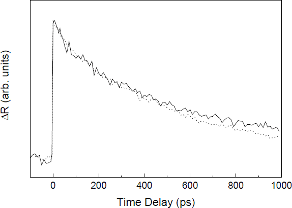
Figure 2 Normalized change in probe reflectivity ΔR as a function of time delay between pump and probe pulses with center wavelength λ=357.5 nm. Dotted line: carrier density n=2×1019cm−3; dashed line: n=1×1019cm−3; solid line: n=3.3×1018cm−3; dash-dotted line: n=1.3×1018cm−3.

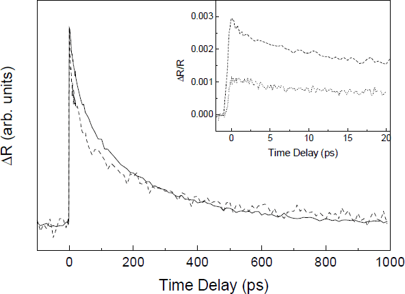
Figure 3 Normalized change in probe reflectivity ΔR as a function of time delay between pump and probe pulses with center wavelength λ=347 nm. Solid line: carrier density n=4×1019cm−3; dashed line: n=4.5×1018cm−3. Inset: ΔR/R at short time delays for carrier densities of n=4.5×1018cm−3 (dashed line) and n=2.2×1018cm−3 (dotted line).
For excitation at 357.5 nm, the electrons possess less than 50 meV of excess energy above the conduction band edge. In this case the ΔR decays become faster as the carrier density is lowered. Using the time at which ΔR reaches half its maximum value as a measure of the decay time τhm, we find that τhm is about 5 times shorter (∼46 ps) for the lowest carrier density data shown in figure 2 (dash-dotted line) than for the highest density data (∼226 ps, dotted line).
Figure 3 shows ΔR data for excitation at 347 nm. In this case the initial excess energy of the electron distribution is greater than 100 meV, exceeding the LO phonon energy of 92 meV. As observed in figure 2, the ΔR decay becomes faster with decreasing excitation density, with τhm dropping by nearly a factor of 2, from 67 ps to 35 ps, when the carrier density is lowered by nearly an order of magnitude. The inset of figure 3 shows that the curve obtained for the lower carrier density in the main figure possesses an initial rapid decay with a 1.25 ps time constant. Upon reducing the carrier density by an additional factor of 2, this initial decay disappears (dotted line, inset).
Discussion
For resonant excitation of A(B) excitons, photoinduced bleaching of the excitonic absorption creates a primarily positive ΔR [Reference Hess, Walraet, Taylor, Ryan, Beaumont and Gibart6]. The decay of this ΔR can be associated with the removal of free excitons by recombination or trapping at deep levels. The fact that the slow decay in figure 1 becomes only slightly faster when the intensity is increased by about an order of magnitude implies that the decay of ΔR for our sample is due to recombination rather than trapping, as saturation of deep level traps with increasing intensity would slow the decay of excitons [Reference Haag, Hönerlage, Briot and Aulombard7]. Noting that the spot size of the probe is ∼100 μm in diameter, comparison of the ratio of the decay components C2/ C1 to the ratio of stripe size to window size suggests that the slow τ2 decay may represent the exciton lifetime in the LEO material, while the fast τ1 decay may be characteristic of the highly defective window region. Low temperature ΔR studies of resonantly excited exciton dynamics in LEO metalorganic vapor phase epitaxy (MOVPE) material [Reference Hess, Walraet, Taylor, Ryan, Beaumont and Gibart6] and time-resolved photoluminescence (TRPL) studies of hydride vapor phase epitaxy (HVPE) material [Reference Bunea, Herzog, Ünlü, Goldberg and Molnar8] yield free exciton lifetimes of 375 ps at 60 K and 295 ps at 4 K, respectively. These results are in good agreement with theoretical predictions of the radiative lifetime [Reference Toyozawa9]. At room temperature the exciton lifetime is longer (∼720 ps) in our MOCVD-grown LEO material than that reported (530 ps) for the high quality HVPE sample, with the long lifetimes in both cases associated with a thermally induced increase in the center of mass kinetic energy of the excitons. While the τ1 of 55 ps in our LEO sample is consistent with decay times observed in more defective GaN films, it is important to note that TRPL measurements capable of discriminating between the window and high quality materials [Reference Chichibu, Marchand, Minsky, Keller, Fini, Ibbetson, Fleischer, Speck, Bowers, Hu, Mishra, DenBaars, Deguchi, Sota and Nakamura10] yielded a dominant decay time of 130 ps for both cases when excitation pulses of 4.64 eV photon energy were employed.
The fact that ΔR possesses a positive rise near zero time delay for excitation of free carriers at 357.5 nm or 347 nm is indicative of the rapid thermalization of the electrons through electron-electron scattering, which causes the distribution to be weighted toward energies below the center of the probe spectrum (equation 1). Since the results described above imply that saturation of defect-related traps does not play an important role in the exciton dynamics, we propose that the ΔR decays for 357.5 nm excitation are primarily associated with the Coulomb capture of electron-hole pairs to form excitons. As the carrier density increases, the Coulomb interaction is more efficiently screened and the decay of the electron distribution is retarded. Viewed in this way, the decay time τhm ∼46 ps at the lowest excitation density (∼1018cm−3) becomes the exciton formation (capture) time at that carrier density.
Comparison of figures 2 and 3 shows that the ΔR decays are much faster at a given carrier density for 347 nm excitation than for the 357.5 nm data. For the 347 nm case, the hot electron distribution cools primarily by transfer of energy to both the cold photoexcited hole distribution through electron-hole scattering, and to the lattice through electron-LO phonon scattering. At high excitation density (solid line, fig. 3) the slow decay suggests that the electron-LO phonon interaction is strongly screened, and the τhm of ∼67 ps represents the relaxation time associated with electron-hole scattering at this carrier density. The fact that the decay time is nearly halved when the carrier density is reduced by almost an order of magnitude (dashed line) implies that the partially screened electron-LO phonon interaction begins to play a role in the cooling process. This observation is supported by the data at short times (inset), for which the initial 1.25 ps decay at this carrier density is attributed to the screened electron-LO phonon interaction. The absence of this initial decay when the carrier density is further lowered to ∼2×1018cm−3 suggests that the screening is attenuated enough that the initial relaxation process becomes faster than the temporal resolution of our experiment (∼200 fs), in agreement with the results of other researchers [Reference Tsen, Ferry, Botchkarev, Sverdlov, Salvador and Morkoc11].
Conclusions
We have demonstrated that picosecond photoinduced reflectivity measurements can be used to obtain information about room temperature exciton and free carrier dynamics in LEO GaN. For resonant excitation of cold excitons, the ΔR decay possesses a 720 ps component attributed to the free exciton lifetime in this high quality material. For electrons with small excess energy (< 50 meV), the strong increase in the ΔR decay rate with decreasing excitation density suggests that screening of the Coulomb interaction may play an important role in the processes of carrier relaxation and exciton formation. The faster decay times at a given carrier density observed for hot (> 100 meV) electron relaxation are attributed to electron-hole scattering in conjunction with the screened electron-LO phonon interaction.
Acknowledgements
The authors thank NSF, ONR, and the State of Texas for partial support of this work at UT-Austin.