


Introduction
All of III-V nitride-based light-emitting diodes (LEDs) [Reference Nakamura, Senoh, Iwasa, Nagahama, Yamada and Mukai1-Reference Mukai, Narimatsu and Nakamura3] and laser diodes (LDs) [Reference Nakamura, Senoh, Nagahama, Iwasa, Yamada, Matsushita, Kiyoku and Sugimoto4,Reference Nakamura and Fasol5] use an InGaN active layer instead of a GaN active layer because of the difficulty in fabricating highly efficient light-emitting devices using a GaN active layer. Highly efficient UV/blue/green/amber InGaN quantum-well structure LEDs have been fabricated directly on a sapphire substrate in spite of a high dislocation density of 1-10 × 1010 cm−2 originating from a large lattice mismatch between GaN and the sapphire substrate [Reference Nakamura, Senoh, Iwasa, Nagahama, Yamada and Mukai1-Reference Mukai, Narimatsu and Nakamura3]. Due to the high efficiency of the LEDs grown on the sapphire substrates, the dislocations in InGaN do not appear to work as a nonradiative recombination center [Reference Lester, Ponce, Craford and Steigerwald6]. Epitaxially laterally overgrown GaN (ELOG) on sapphire was developed recently to reduce the number of threading dislocations in the GaN epitaxial layers [Reference Usui, Sunakawa, Sakai and Yamaguchi7,Reference Nam, Bremser, Zheleva and Davis8]. Using the ELOG, the number of threading dislocations was reduced significantly in the GaN grown on the SiO2 mask. Thus, there is a great interest in fabricating LEDs and LDs using the ELOG substrate which has a small number of dislocations in order to study the role of the dislocations in the InGaN-based LEDs and LDs. For the study, blue InGaN single-quantum-well (SQW) structure LEDs were fabricated on the ELOG and sapphire substrates [Reference Mukai, Takekawa and Nakamura9]. The LDs were formed on the SiO2 mask and window regions of the ELOG substrate [Reference Nakamura, Senoh, Nagahama, Iwasa, Yamada, Matsushita, Kiyoku, Sugimoto, Kozaki, Umemoto, Sano and Chocho10]. Also, the LD was grown on the free-standing GaN substrate which was obtained by removing the sapphire substrate after growing a thick ELOG substrate [Reference Nakamura, Senoh, Nagahama, Iwasa, Yamada, Matsushita, Kiyoku, Sugimoto, Kozaki, Umemoto, Sano and Chocho11]. In addition, present performance of InGaN-based LEDs and LDs are described.
Blue LEDs on Elog and Sapphire Substrates
Selective growth of GaN was performed on a 2-µm-thick GaN layer grown on a (0001) C-face sapphire substrate. The 0.1-µm-thick silicon dioxide (SiO2) mask was patterned to form 3-µm-wide stripe windows with a periodicity of 9 µm in the GaN <1-100> direction. Following the 7-µm-thick GaN growth on the SiO2 mask pattern, the coalescence of the selectively grown GaN enabled the achievement of a flat GaN surface over the entire substrate. This coalesced GaN was designated the ELOG. We examined the defect density by plan-view transmission electron microscopy (TEM) observations of the ELOG substrates.
Figure 1 shows plan-view TEM image of the surface of the ELOG substrate with a thickness of 7 µm. The number of threading dislocations (TDs) on the SiO2 mask area was lower than 1 × 106 cm−2, and that on the window area was approximately 3 × 107 cm−2. The TD density of conventional GaN which was grown directly on the sapphire substrate without the ELOG was of the order of 1 × 1010 cm−2 [Reference Lester, Ponce, Craford and Steigerwald6], the number of the TDs was reduced considerably when the ELOG substrate was used. After obtaining a 15-µm-thick ELOG substrate, an InGaN SQW blue LED structure was grown on the substrate in order to study a role of the dislocations. The LED structure was already described previously [Reference Mukai, Takekawa and Nakamura9]. The characteristics of the LEDs were measured under a direct current (DC) at room temperature. For a comparison, blue LED with the same structure was also fabricated directly on the sapphire substrate without the ELOG.

Fig. 1. Plan-view TEM image of the surface of the ELOG substrate with a thickness of 7 µm.
Figure 2 show a photograph of real LED on ELOG under a forward current of 3 mA. This photograph was taken using a microscope. The size of each LED chip is as large as 350 µm x 350 µm. Each LED chip includes many window and SiO2 stripe regions periodically. No inhomgeneties of blue emission intensity over the entire surface of the p-type transparent Ohmic contact layer was observed. Thus, it is concluded that a large number of TDs of 3 × 107 cm −2 on the widow region do not serve to decrease the efficiency of the LEDs. The ELOG and GaN on sapphire had average TD densities of 1 × 107 cm−2 and 1 × 1010 cm−2, respectively. Here, average TD density of the ELOG on sapphire was obtained by dividing the TD density of 3 × 107 cm−2 on the window region by the ratio of (stripe periodicity of 9 µm)/ (window width of 3 µm) because the TD density on the SiO2 stripe region was lower than 1 × 106 cm−2, as shown in Fig. 1.

Fig. 2. Photograph of blue InGaN SQW LED on ELOG under a forward current of 3 mA.
The output power of both LEDs at a current of 20 mA was 6 mW, which is equal to the external quantum efficiency of 11 %. In spite of a large number of dislocations, the LED on sapphire had the same output power as that on ELOG. Thus, the dislocation seems not to work as nonradiative recombination centers in the InGaN active layer. If the TDs work as nonradiative recombination centers, the output power of the LED on ELOG have to be much higher than that on sapphire due to a small number of average TD density.
Figure 3 shows the emission spectra of the blue InGaN SQW LEDs on ELOG at forward currents from 0.1 mA to 20 mA. At a current of 20 mA, the peak wavelength and the full-width at half maximum (FWHM) of the emission spectra of the LED on ELOG were 470 nm and 27 nm, respectively, and those on sapphire were 464 nm and 26 nm, respectively. The peak wavelength of the LED on ELOG is somewhat longer than that on sapphire probably due to a growth fluctuation. There is no significant difference between in the spectra of both LEDs. The broad spectral width is mainly due to an In composition fluctuation in the InGaN well layer [Reference Chichibu, Azuhata, Sota and Nakamura12-Reference Narukawa, Kawakami, Funato, Fujita, Fujita and Nakamura14]. This means that the size of the fluctuation is the same in both LEDs in spite of a large difference in the dislocation density. Thus, the In composition fluctuations are not related to the dislocations. In the spectra, the blueshift is easily observed due to a band-filling effect of the deep localized energy states. The blue LED on sapphire also showed the same blueshift with increasing the forward current. We measured the absorption spectra and electroluminescence (EL) of blue/green InGaN SQW LEDs grown on sapphire substrate in previous studies [Reference Chichibu, Azuhata, Sota and Nakamura12-Reference Narukawa, Kawakami, Funato, Fujita, Fujita and Nakamura14]. The entire EL appeared at the lower energy tail of the absorption spectra. The EL of blue and green LEDs originated from the carrier recombination at the deep localized energy states with a localization energy of 290 meV and 570 meV, respectively. The blueshift of the EL of the green SQW LEDs with increasing forward current was due to a band-filling effect of the localized energy states. Both LEDs showed the same peak wavelength dependence on the current, which implies the same blueshifts. Thus, the TDs are not directly related to the formation of the localized energy states. These localized states are probably formed by the In composition fluctuation in the InGaN well layer due to a natural phase separation of InGaN during growth. Therefore, assuming that the localized states are formed by the In composition fluctuation in the InGaN well layer, the TD related composition fluctuation is eliminated because the TD density of the epilayer on the ELOG is relatively small.
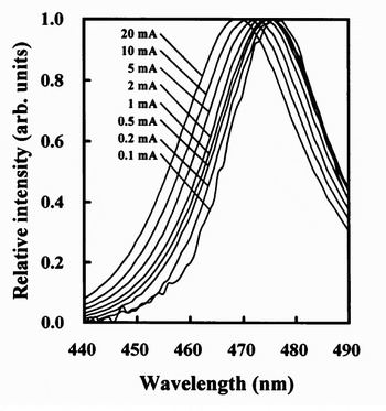
Fig. 3. Emission spectra of blue InGaN SQW LED grown on ELOG substrate at various forward currents.
Thus, the localization induced by the In composition fluctuations seem to be a key role of the high efficiency of the InGaN-based blue LEDs. When the electrons and holes are injected into the InGaN active layer of the LEDs, these carriers are captured by the localized energy states before they are captured by the nonradiative recombination centers caused by the large number of TDs [Reference Nakamura15]. It was reported that the TDs served as a nonradiative recombination center in GaN and InGaN [Reference Rosner, Carr, Ludowise, Girolami and Erikson16,Reference Sugahara, Sato, Hao, Naoi, Kurai, Tottori, Yamashita, Nishino, Romano and Sakai17]. These localized energy states can be formed only in InGaN films during the growth due to a phase separation of the InGaN. Assuming that the lateral spacing of the effective bandgap (potential) minimum due to the In composition determines the carrier diffusion length in InGaN, the diffusion length was estimated to be less than 60 nm from the spatially resolved CL spectrum mapping measurement [Reference Chichibu, Wada and Nakamura18]. It was also concluded that the efficiency of light emission was high as long as the minority carrier diffusion length was shorter than the dislocation spacing [Reference Chichibu, Wada and Nakamura18]. Considering about these previous results, the carrier diffusion length determined by the potential fluctuation due to InGaN phase separation must be less than the TD spacing in the InGaN layer in order to obtain high-efficient InGaN-based LEDs.
Figure 4 shows the reverse biased I-V characteristics of both LEDs. At a reverse bias voltage of −20 V, the reverse current of the LED on the ELOG was 0.009 µA, and that on sapphire was 1 µA. Under the reverse biased condition, the LED on sapphire had a considerable amount of leakage current. This leakage current is probably caused by the TDs because the LEDs on sapphire have a considerable amount of leakage current and many TDs [Reference Sasaoka, Sunakawa, Kimura, Nido, Usui and Sakai19].

Fig. 4. I-V characteristics of blue InGaN SQW LEDs grown on ELOG and on sapphire substrates under reverse biased conditions.
InGaN-Based Red LEDs
We also fabricated red InGaN SQW LEDs by increasing the In composition and thickness of InGaN well layers in the above LED structure. The In composition and thickness of the InGaN well layer were changed to approximately 50 % and 40Å, respectively. Here, the In composition was determined assuming that the bowing parameter of InGaN was 1 eV [Reference Osamura, Naka and Murakami20]. However, recent studies revealed that the bowing parameter of InGaN is much higher than 1 eV [Reference Amano, Takeuchi, Sota, Sakai and Akasaki21,Reference McCluskey, Van de Walle, Master, Romano and Johnson22]. In that case, the In content in the InGaN layer should be much smaller than the above values. The LED structure was grown directly on a sapphire substrate without ELOG. Figure 5 shows the emission spectrum of red InGaN SQW LED at a forward current of 5 mA. The peak wavelength is 650 nm (1.91 eV), which peak emission energy is almost equivalent to a band-gap energy of InN. When the current was changed from 5 mA to 80 mA, a large blueshift of the peak wavelength was observed from 650 nm to 580 nm. Because of low symmetry, the wurtzite system such as InGaN-based materials, displays pyroelectric and piezoelectric behavior [Reference Chichibu, Azuhata, Sota and Nakamura23-Reference Im, Kollmer, Off, Sohmer, Scholz and Hangleiter26]. The macroscopic polarization in the material comprising the active region of the SQW or MQW structure gives rise to a net electric field perpendicular to the plane of the well. This field, if strong enough, will induce a spatial separation of the electron and hole wave functions in the well. As the charge density becomes concentrated near the walls of the well, the wave function overlap decreases and the interband recombination rate decrease (the quantum-confined Stark effect (QCSE)). The blueshift of the electroluminecence (EL) of the InGaN SQW LEDs with increasing operating current can be explained by the QCSE resulting from piezoelectric fields [Reference Im, Kollmer, Off, Sohmer, Scholz and Hangleiter26], when the In composition and thickness of the InGaN well layer are large. However, a higher efficiency of the LEDs with increasing strain in the SQW upon increasing the In content in the InGaN well layers, was observed from UV to green LEDs [Reference Nakamura, Senoh, Iwasa, Nagahama, Yamada and Mukai1,Reference Mukai, Morita and Nakamura2,Reference Nakamura and Fasol5]. These phenomena cannot be explained by only the QCSE. It may be that the localization effects induced by composition fluctuations must overcome these intrinsic limitations due to the piezoelectric field. Considering about previous works, the emission wavelength of the red LED dependence on the current (blueshift) is mainly dominated by the screening effects of the QCSE due to the large In composition and thickness of the InGaN well layer.

Fig. 5. Emission spectrum of red InGaN SQW LED grown on sapphire substrate.
Violets LDs Grown on Elog Substrates
The LDs with an InGaN MQW/GaN/AlGaN separate confinement heterostructure (SCH) was grown on above-mentioned ELOG substrate. To grow the thick AlGaN cladding layer with a high Al content required for optical confinement without any cracks, GaN/AlGaN modulation doped strained-layer superlattices (MD-SLSs) within the range of critical thickness instead of thick AlGaN layers were used as cladding layers [Reference Nakamura, Senoh, Nagahama, Iwasa, Yamada, Matsushita, Kiyoku, Sugimoto, Kozaki, Umemoto, Sano and Chocho10,Reference Nakamura, Senoh, Nagahama, Iwasa, Yamada, Matsushita, Kiyoku, Sugimoto, Kozaki, Umemoto, Sano and Chocho11]. The LD structure was grown on the ELOG substrate with a thickness of 15 µm. The InGaN MQW LD device consisted of a 3-µm-thick layer of n-type GaN:Si, a 0.1-µm-thick layer of n-type In0.1Ga0.9N:Si, a Al0.14Ga0.86N/GaN MD-SLS cladding layer consisting of 120 25-Å-thick undoped GaN separated by 25-Å-thick Si-doped Al0.14Ga0.86N layers, a 0.1-µm-thick layer of Si-doped GaN, an In0.15Ga0.85N/In0.02Ga0.98N MQW structure consisting of four 35-Å-thick Si-doped In0.15Ga0.85N well layers forming a gain medium separated by 105-Å-thick Si-doped In0.02Ga0.98N barrier layers, a 200-Å-thick layer of p-type Al0.2Ga0.8N:Mg, a 0.1-µm-thick layer of Mg-doped GaN, a Al0.14Ga0.86N/GaN MD-SLS cladding layer consisting of 240 25-Å-thick undoped GaN separated by 25-Å-thick Mg-doped Al0.14Ga0.86N layers, and a 0.05-µm-thick layer of p-type GaN:Mg. The 0.1-µm-thick n-type and p- type GaN layers were light-guiding layers. The n-type and p-type Al0.14Ga0.86N/GaN MD-SLS layers acted as cladding layers for confinement of the carriers and the light emitted from the active region of the InGaN MQW structure. The structure of the ridge-geometry InGaN MQW LD was almost the same as that described previously [Reference Nakamura and Fasol5,Reference Nakamura, Senoh, Nagahama, Iwasa, Yamada, Matsushita, Kiyoku, Sugimoto, Kozaki, Umemoto, Sano and Chocho10,Reference Nakamura, Senoh, Nagahama, Iwasa, Yamada, Matsushita, Kiyoku, Sugimoto, Kozaki, Umemoto, Sano and Chocho11]. First, the surface of the p-type GaN layer was partially etched until the n-type GaN layer and the p-type Al0.14Ga0.86N/GaN MD-SLS cladding layer were exposed, in order to form a ridge-geometry LD. The laser cavity was formed parallel to the direction of the SiO2 stripe. A mirror facet was formed by dry etching, as reported previously [Reference Nakamura and Fasol5]. High-reflection facet coatings (90 %) consisting of 2 pairs of quarter-wave TiO2/SiO2 dielectric multilayers were used to reduce the threshold current. A Ni/Au contact was evaporated onto the p-type GaN layer, and a Ti/Al contact was evaporated onto the n-type GaN layer. The electrical characteristics of the LDs fabricated in this way were measured under a direct current (DC). The structure of the LD is shown in Fig. 6.

Fig. 6. Structure of the InGaN MQW-structure LDs with MD-SLS cladding layers grown on the ELOG substrate.
The ridge-geometry LDs were formed on the GaN layer above the SiO2 region with low TDs of lower than 1 × 106 cm−2 and the window region with a high TD density of 3 × 107 cm−2. The V-I characteristics and the light output power per coated facet of the LD with a cavity length of 450 µm and a ridge width of 4 µm as a function of the forward DC current (L-I) at RT were measured. When the LD was formed on the GaN layer above the SiO2 mask region with low TDs, the threshold current was 53 mA, which corresponded to a threshold current density of 3 kAcm−2. When the LD was formed on the window region with the high TD density, the LD had a threshold current density of 6 to 9 kAcm−2, which was much higher than that of the LD formed on the SiO2 mask. The higher threshold current density is probably caused by the large number of TD density of 3 × 10 7 cm−2 at the window region. It was confirmed that the dislocation served as a leakage current pathway in InGaN as shown in Fig. 4. Thus, there is a possibility that a leakage current due to a large number of TDs caused the high threshold current density on the window region. Further studies are required to determine the exact reasons of the high threshold current density caused by TDs.
Figure 7 shows the results of a lifetime test for CW-operated LDs formed on the GaN layer above the SiO2 mask region carried out at 20˚C, in which the operating current is shown as a function of time under a constant output power of 2 mW per facet controlled using an autopower controller (APC). The LDs is survived 9,800 hours of operation. The LDs formed on the window region showed the lifetimes of 1,000-3,000 hours due to the high threshold current density of 6 to 9 kAcm−2. The emission spectra of the LDs were measured under RT-CW operation at currents of 50 and 60 mA, as shown in Fig. 8. At a current of 50 mA, longitudinal modes with a mode separation of 0.04 nm due to the cavity were observed. At a current of 60 mA, a single-mode emission was observed at an emission wavelength of 396.6 nm.

Fig. 7. Operating current as a function of time under a constant output power of 2 mW per facet controlled using an autopower controller. The InGaN MQW LDs with MD-SLS cladding layers grown on the ELOG substrate were operated under DC at 20˚C.

Fig. 8. Laser emission spectra measured under RT CW operation with currents of 50 mA and 60 mA.
High-power LDs were also fabricated on the ELOG substrate. After obtaining a 20-µm-thick ELOG substrate, the InGaN MQW LD structure was grown on the surface. The InGaN MQW LD structure was the same as described in Fig. 6 except for the active layer. The InGaN MQW structure was changed to an In0.15Ga0.85N/In0.02Ga0.98N MQW structure consisting of two 40-Å-thick undoped In0.15Ga0.85N well layers forming a gain medium separated by 100-Å-thick Si-doped In0.02Ga0.98N barrier layers. The area of the ridge-geometry LD was 3 µm x 450 µm. A laser cavity was formed by cleaving the facets along {1-100} of the LD grown on the ELOG substrate after polishing the sapphire substrate to 70 µm. A facet coating (90 %) consisting of 2 pairs of quarter-wave TiO2/SiO2 dielectric multilayers was formed on one side of the facet. The output power of the LD was measured from the other side of uncoated facet.
Figure 9 shows the V-I characteristics and the light output power per uncoated cleaved facet of the LD grown on the ELOG substrate with a number of well of 2 as a function of the forward DC current (L-I) at RT. No stimulated emission was observed up to a threshold current of 40 mA, which corresponds to a threshold current density of 3 kA/cm2. The slope efficiency was as high as 1.2 W/A per facet because the output power was measured from the uncoated cleaved mirror facet having low reflectivity. The differential quantum efficiency per facet was 39 %. The output power of the LDs was as high as 420 mW at an operating current of 490 mA. This output power is the highest ever reported for III-V nitride-based LDs under RT-CW operation. At an output power of 100 mW, a kink was observed in the L-I curve because the transverse mode change occurred at an output power of 100 mW. The emission spectra of the LDs were measured under RT-CW operation at output powers of 10 mW and 30 mW. At output powers of 10 mW and 30 mW, stimulated emission was observed at wavelengths of around 408.2 and 408.8 nm, respectively. The lifetime test of the high-power LD was carried out at an ambient temperature of 50˚C and a constant output power of 30 mW controlled using the APC. The initial operating current was as high as 100 mA due to the high-temperature operation. A small increase in the operating current was observed with increasing operation time. After 250 hours of operation, the operating current increases dramatically. Thus, the lifetime of the LD was 250 hours.

Fig. 9. Typical L-I and V-I characteristics of InGaN MQW LDs measured under CW operation at RT.
LDs Grown on GaN Substrates
After obtaining a 20-µm-thick ELOG substrate, the wafer was removed from the MOCVD reactor. Next, GaN growth was carried out using a conventional hydride vapor phase epitaxy (HVPE) system using a horizontal quartz reactor because the growth rate of GaN is much higher when using the HVPE method. Undoped GaN growth was continued up to 200 µm. Then, the sapphire substrate was removed by polishing, in order to obtain a pure GaN substrate with a thickness of approximately 150 µm. Then, the InGaN MQW LD structure was grown on the surface of the 150-µm-thick GaN substrate by MOCVD. The InGaN MQW LD structure was the same as described in Fig. 6 except for the active layer. The InGaN MQW structure was changed to an In0.15Ga0.85N/In0.02Ga0.98N MQW structure consisting of two 40-Å-thick undoped In0.15Ga0.85N well layers forming a gain medium separated by 100-Å-thick Si-doped In0.02Ga0.98N barrier layers. The area of the ridge-geometry LD was 3 µm × 400 µm. A laser cavity was formed by cleaving the facets along {1-100} of the LD grown on the GaN substrate. A facet coating (90 %) consisting of 2 pairs of quarter-wave TiO2/SiO2 dielectric multilayers was formed on one facet. The output power of the LD was measured from another uncoated facet.
Figure 10 shows the V-I characteristics and the light output power per uncoated cleaved facet of the LD grown on the GaN substrate as a function of the forward DC current (L-I) at RT. No stimulated emission was observed up to a threshold current of 80 mA, which corresponds to a threshold current density of 7 kA/cm2. The slope efficiency was as high as 0.8 W/A per facet because the output power was measured from the uncoated cleaved mirror facet having low reflectivity. The differential quantum efficiency per facet was 26 %. The output power of the LDs was as high as 160 mW at an operating current of 300 mA. At an output power of 80 mW, a kink was observed in the L-I curve because the transverse mode change occurred at an output power of 80 mW.

Fig. 10. Typical L-I and V-I characteristics of InGaN MQW LDs grown on GaN substrate measured under CW operation at RT.
Figure 11 shows near-field patterns (NFP) of the LDs taken by a charge-coupled device (CCD) camera through the optical microscope at output powers of 70 mW and 100 mW. The fundamental transverse mode was observed below the output power of 80 mW, as shown in Fig. 11(a). With increasing output power above 80 mW, the first-order transverse mode appeared, as shown in Fig. 11(b). This transverse mode change at an output power of 80 mW caused the kink in the L-I curve. In order to suppress the change, we must control the transverse mode to be a fundamental mode, by further narrowing the ridge width.

Fig. 11. Near-field pattern of InGaN MQW LDs at output powers of (a) 70 mW and (b) 100 mW under RT-CW operation. X and Y directions are parallel and perpendicular to the junction of the LD, respectively
The emission spectra of the LDs were measured under RT-CW operation at output powers of 3 mW, 10 mW and 40 mW. At an output power of 3 mW, longitudinal modes with many sharp peaks due to a cavity with a length of 400 µm, were observed. At output powers of 10 mW and 40 mW, multimode emission was observed at wavelengths of around 410.5 and 411.3 nm, respectively. The lifetime test was performed under CW-operation at an ambient temperature of 50˚C and a constant output power of 5 mW controlled using the APC. The initial operating current was as high as 160 mA due to the high-temperature operation. After 180 hours of operation, the operating current increased dramatically. The lifetime was about 180 hours due to a high threshold current density of 14 kAcm−2.
Conclusions
InGaN quantum-well-structure blue LEDs were grown on ELOG and sapphire substrates. The LED on sapphire had a considerable amount of leakage current in comparison with that on ELOG. These results indicate that In composition fluctuation is not caused by TDs, free carriers are captured by radiative recombination centers before they are captured by nonradiative recombination centers in InGaN, and that the dislocations form the leakage current pathway in InGaN. Red LED with an emission peak wavelength of 650 nm was fabricated by increasing the In composition and thickness of InGaN well layer. When the LD was formed on the GaN layer above the SiO2 mask region, the threshold current density was as low as 3 kAcm−2. When the LD was formed on the window region, the threshold current density was as high as 6 to 9 kAcm−2. There is a possibility that a leakage current due to a large number of TDs caused the high threshold current density . The longest lifetime of 9,800 hours at a constant output power of 2 mW was achieved. InGaN MQW LDs were fabricated on a GaN substrate grown by HVPE. The fundamental transverse mode was observed up to an output power of 80 mW. These results indicate an imminent commercialization of the LDs in the near future.


