


 . For bulk crystals n
1. Introduction
Due to its material properties gallium nitride (GaN) has attracted enormous attention in recent years, certainly after the success of GaN-based blue-light emitting diodes. The lack of lattice-matched substrates for epitaxial growth of GaN films has led to the application of a variety of substrates of which sapphire is most abundantly used Reference Ponce, Moustakas, Akasaki and Monemar[1]. Despite the large mismatch in the lattice constants between GaN and sapphire, a two-step growth process, proposed by Amano et al. Reference Amano, Sawaki, Akasaki and Toyoda[2], makes it possible to grow device quality hetero-epitaxial GaN layers. However, these layers are still highly defective thereby degrading device performance. GaN single crystals would provide perfect lattice matched substrates which can be easily cleaved. Although considerable progress has been made in increasing the size of the GaN single crystals Reference Porowski[3], at present, their relatively small crystal-size is still a bottleneck for the application as lattice matched substrate.
Ellipsometry has been used by several authors Reference Edwards, Bremser, Weeks, Kern and Davis[4] Reference Petalas, Logothetidis, Boultadakis, Alouani and Wills[5] Reference Yu, Wang, Ishikawa, Umeno, Soga, Egawa, Watanabe and Jimbo[6] Reference Yu, Ishikawa, Egawa, Soga, Watanabe, Jimbo and Umeno[7] to study GaN. It is a non-destructive technique which can be performed on optically flat surfaces of almost any material in order to study surface as well as bulk properties. If polarised light is reflected from the sample at an angle of reflection φ, the reflected beam will be elliptically polarised. Dividing the p-polarised component by the s-polarised component one can define two ellipsometric quantities Δ and Ψ, given by,
The two parameters, Δ and Ψ, contain information on the sample as thickness and refractive index of the film. They are very sensitive to the presence of overlayers on the surface of the material such as a natural oxide layer or a rough surface layer Reference Kuphal and Dinges[8] Reference van Hasselt[9]. In this paper ellipsometry was applied for the characterisation of GaN single crystals obtained by the high pressure technique Reference Porowski[3] and GaN layers grown on sapphire. For the hetero-epitaxial films a multilayer model is used, in which the real and the imaginary part of the complex refractive index as well as the film thickness are fitted simultaneously from the (Δ,Ψ)-spectra. The results were compared with the data obtained from the GaN single crystals.
2. Experimental
Undoped GaN layers were grown on two inch sapphire (0001) substrates using a horizontal metalorganic chemical vapour deposition (MOCVD) reactor. Immediately before growth, the substrates were cleaned in organic solvents, etched in a solution of HCl:HNO3 = 3:1, rinsed with de-ionised water, and blown dry with filtered N2 gas. After nitridation of the substrate surface, carried out in a ammonia (NH3) gas stream at 1030°C, the temperature was lowered to 500°C and a 20 nm thick GaN buffer was deposited. On this buffer, a 1.5 μm thick GaN layer was grown at a temperature of 1050°C and a pressure of 50 mbar using trimethylgallium (TMG) and NH3 as precursors, and H2 as carrier gas. Growth was performed with a TMG flow of about 60 μmol/min and a NH3 flow of 2.5 slm, diluted with H2 to a total flow of about 5 slm. The GaN epilayers on sapphire have a mirror smooth surface and were found to be of Ga-polarity, according to selective etching experiments Reference Weyher, Müller, Grzegory and Porowski[10].
Unintentially n-doped GaN single crystals were grown from nitrogen and liquid gallium under nitrogen pressures close to 15 kbar and at temperatures higher than 1500°C Reference Porowski[3] Reference Krukowski[11]. Before ellipsometry was performed the as-grown single crystals were polished with diamond paste (0.1 μm) to remove a visible surface layer resulting from the transition from growth to ambient conditions. The side of gallium polarity was found to be unaffected by chemical etchants, only the side of nitrogen polarity can be mechano-chemically polished with aqueous solutions of NaOH and KOH Reference Weyher, Müller, Grzegory and Porowski[10]. As a result of this anisotropic behaviour, the roughness of the N-polarity side is lower which makes it more suitable for ellipsometry.
Ellipsometric measurements were performed with two experimental set-ups. A Gaertner L117C ellipsometer was used to measure the ellipsometric angles Δ and Ψ at the HeNe-laser wavelength of λ = 632.8 nm. The spotsize of the laser beam is 1 mm in diameter. The measurements were carried out at an angle of incidence of 70.00° ± 0.02°. Spectroscopic ellipsometry (SE) was measured by a four zone spectrometer Reference van Hasselt[9] Reference Azzam and Bashara[12] in the region 240 nm − 840 nm with a resolution of 2 meV or 0.2 nm at the bandgap. A Xenon lamp was used as light source, the spotsize during measurements was 1 mm in diameter, the angle of incidence was the same as for the single wavelength ellipsometer. The values of Δ and Ψ are measured with a typical precision of ± 0.02°. All measurements were performed at room temperature.
3. Results and discussion
Since different hetero-epitaxial layers grown under similar conditions gave comparable results, data from a characteristic sample, referred to as GaN-C, were chosen to be analyzed in detail.
Determination of the GaN film thickness over the wafer shows a thickness variation of about one percent, as can be seen in Figure 1. These results are confirmed by the shift of the peaks seen in the s-reflection spectra (362 nm − 840 nm) for different positions on the sample.
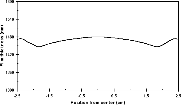
Figure 1. A thickness profile of the hetero-epitaxial GaN layer (GaN-C) obtained by single wavelength ellipsometry.
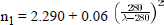
In a first approximation the maxima and minima in the s-reflection, in the transparent region 362 nm − 840 nm, were analysed using a Cauchy-type of dispersion, in which the real part of the refractive index n1 is given by:
and the imaginary part of the refractive index n2 is set to zero. In the above equation A, B, and C are fitting parameters and λ is the wavelength of light in nanometers. Furthermore the buffer is not treated as separate layer but as part of the epitaxial GaN film. The best fit for the measured data was obtained for A = 2.290, B = 0.05, and C = 280 nm. The corresponding film thickness d of 1470 ± 20 nm, is within the accuracy of the average-thickness determination by gravimetry, 1482 ± 12 nm (assuming only deposition of wurtzite GaN on top of the substrate), from which can be concluded that a first ellipsometric approach is sufficient for accurate and non-destructive layer thickness determination. In order to study the stability of hetero-epitaxial grown GaN film, the GaN-C sample was investigated at two subsequent times with an one-month interval. SE was performed near the centre of the samples at energies about the gap of GaN ( Figure 2). The measurements show that no detectable change of the GaN surface occurs within this one-month period, in contrast to materials like GaAs where a continual oxidation of the surface takes place Reference Kuphal and Dinges[8]. In Figure 2 a small shift of the ellipsometric angles Δ and Ψ at the two subsequent times can be recognised. This shift occurs because there is a small thickness variation over the sample ( Figure 1) and the light beamposition of the second measurement is not exactly the same as of the first measurement (thickness difference < 0.3 nm). A feature in Ψ at λ = 363 nm (3.42 eV) is assumed to be exciton related.
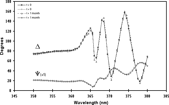
Figure 2. The SE parameters (data points), Δ and Ψ, measured at an angle of incidence of 70.00°, was obtained at two subsequent times with an one-month interval. The lines are a guide to the eye.
A refinement of the results of the first approximation is obtained by a full multilayer description in the transfer matrix formalism Reference Azzam and Bashara[12] of high precision recordings of Δ and Ψ in the region 500 nm − 680 nm, as shown in Figure 3. In this model, the deposited layer on the sapphire substrate is composed of a buffer layer, a GaN epilayer, and a hypothetical overlayer respectively. Furthermore the dispersion of sapphire was set to data found in literature Reference Gray[13], the refractive index of ambient air was taken to be 1.0003, and a thickness of 20 nm for the GaN buffer layer was used, as was determined by transmission electron microscopy.

Figure 3. The SE parameters (data points), Δ and Ψ, measured at an angle of incidence of 70.00°, are fitted (solid line) using a multilayer model.
According to this model, the refractive index n1 was found to follow a Cauchy-type of dispersion as given by Equation 2. The values obtained for the fitting parameters A and C are the same as for the first approximation, while B is found to be 0.06 instead of 0.05. The hypothetical top-layer, if there is any present, is smaller than 1 nm. An overview of the results for sample GaN-C is given in Table 1.
Table 1 A summary of the results of the multilayer model used for GaN-C
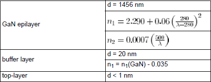
Figure 3 shows that there is an excellent fitting of the SE measurement data and the multi-layer-model simulation, the small difference between model and experiment for λ > 620 nm is thought to be due to a difference in dispersion of the ordinary and extra-ordinary refractive index near 620 nm of substrate or sample, which is not included in the model.
The square of the refractive index of both, the first approximation and the multi layer model, appear to be close to the Sellmeier-type description as given by Yu et al. Reference Yu, Wang, Ishikawa, Umeno, Soga, Egawa, Watanabe and Jimbo[6]. However, it is off by a few percent compared with a subsequent Sellmeier description which was measured on a sample without a buffer layer Reference Yu, Ishikawa, Egawa, Soga, Watanabe, Jimbo and Umeno[7]. Deviations between the various parametric ratios are found particularly in the region 3.5 eV − 4.0 eV, where a single term Sellmeier description appeared not to be sufficient and a next term should be added.
As mentioned before in Section 2, GaN single crystals were polished before SE was performed. Since only the side of nitrogen-polarity could be mechano-chemically polished, resulting in a lower surface roughness, this side was investigated by ellipsometry.
Two mechano-chemically polished samples were studied with ellipsometry at λ = 632.8 nm. It appears that there is an overlayer on top of the samples, which can be a rough surface layer and/or an additional layer of e.g. gallium oxide. Atomic force microscopy reveals that the surface of the single crystals is rough, at least a factor of three rougher than the hetero-epitaxial layers. Assuming that the overlayer is only due to a residual surface roughness, the ellipsometric data indicate that the roughness, given as top-bottom value, is 0.5−2 nm and 1.5−3 nm respectively. This values can be considered as maximum values, which are less in case the overlayer also contains gallium oxide remaining .
The real part of the refractive index at λ = 632.8 nm, averaged over both samples is n1 = 2.337 ± 0.010 which compares well with n1 = 2.328 ± 0.003 of the MOCVD sample. In Table 2 the results for single crystals are compared with those of MOCVD grown GaN. On similar single crystals the absorption coefficient α was measured and found to be ranging from 35 cm−1 − 200 cm−1 betweem 500 nm < λ < 680 nm Reference Suski and Ambacher[14]. This means that
Table 2 Comparison of the results obtained for GaN single crystals and GaN epilayers.

4. Conclusion
Ellipsometry is shown to be a useful technique for characterisation of GaN films and bulk material, it can be used for local film thickness determination. From precision recordings of the ellipsometric quantities (Δ,Ψ) the dispersion of the refractive index is calculated in a full multilayer transfer matrix description. The surfaces of the as-grown hetero-epitaxial layers are smoother than surfaces of the polished single crystals examined in this paper. However, within the experimental error the resulting refractive index of the MOCVD films and high pressure samples are consistent with each other.
Acknowledgments
J. Weyher is acknowledged for the surface treatment of the single crystals. This work has been financially supported by the Dutch Technology Foundation (STW).


