


Introduction
Miniaturization of electronic devices has necessitated probing and exploring electronic transport in semiconductors on the sub-micron and recently the nanometer scale. Similarly, understanding of the functionalities of nanoscale systems, such as 2D materials and carbon nanotubes, requires probing electronic transport, as well as the roles of contacts, internal defects, and interfaces. Comparable problems emerge for ionic conductors, with the added complexity of conversion between electronic and ionic currents at the electrodes. Finally, understanding of mixed electronic-ionic conductors such as used in electrochemical sensors, batteries, and fuel cells requires disentangling electronic and ionic transport from chemical reactions at surfaces, interfaces, and triple-phase junctions.
These considerations have spurred the development of a broad range of electrical characterization techniques, ranging from current-voltage (I-V) and capacitance-voltage (C-V) measurements for transistor characterization to impedance measurements in electrochemistry to more complex strategies for probing polarization switching in ferroelectric non-volatile memories [Reference Ho1–Reference Sze4]. Yet for all the variety of electrical characterization techniques, the probed object ultimately represents a black box. While total integrated response of all structural elements and internal interfaces can be measured, separating individual components represents a complex and often impossible task. For example, measured I-V curves and transconductance responses of the carbon nanotube are a sum of contributions from contacts, internal defects, and even adatoms and traps on the supporting surface (Figures 1a and 1b). As another example, impedance spectroscopy data can be converted to the lumped equivalent circuit comprising resistive, capacitive, and potentially more complex properties, even while the relationship among these aspects and material microstructure represents an open problem. Scanning probe microscopy (SPM) tools for exploring systems with these complexities have been developed and are described in a lecture series.
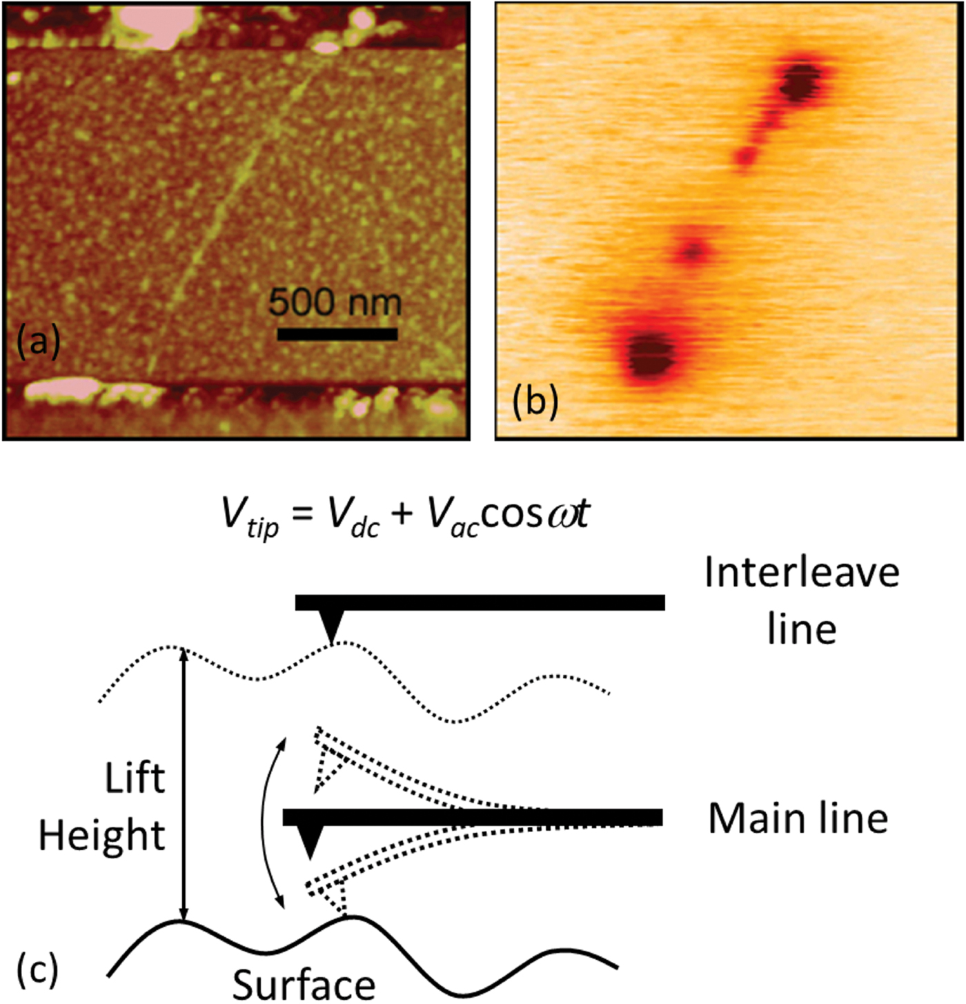
Figure 1: (a) Surface topography and (b) scanning gate microscopy (SGM) image of carbon nanotube circuit. In SGM, the current flowing through the nanotube is measured as a function of the biased tip position, wherein the latter acts as a moving gate electrode. The dark spots on the image indicate the presence of defects at which the tip affects the nanotube conductance strongest. (a,b) are reprinted with permission from [Reference Freitag22]. Copyright 2002 by the American Physical Society. (c) Schematics of Kelvin probe force microscopy. Here, the tip scans the surface and then retraces the surface profile, maintaining constant tip-surface interaction. During this second scan a periodic bias is applied to the tip, and the feedback loop is used to maintain zero oscillation amplitude at the bias frequency. This condition corresponds to the equality of the tip (controlled by the feedback loop) and unknown surface potential, allowing one to map the latter.
Lecture Series on Scanning Probe Microscopy of Electronic and Ionic Transport
This lecture series introduces SPM approaches for probing electronic and ionic transport in nanoscale systems via force, current, and gate effect mechanisms. The first five lectures are focused on applications of Kelvin probe force microscopy, followed by two lectures describing current-voltage measurements and spectroscopies. The lectures are available at YouTube https://www.youtube.com/playlist?list=PLS6ZvEWHZ3OOkRFPTrnsV3Ej09UGUjor3.
Lecture 1
This lecture, “Electronic and ionic transport on the nanoscale: the scanning probe microscopy approach,” introduces the viewer to the general principle of transport measurements and the necessary descriptors including resistance, capacitance, I-V and C-V behavior, and transistor characterization. It proceeds to make the connection between the classical electrical characterization strategies and SPM, where the SPM tip can be used as a moving voltage or current electrode or a moving gate. Compared to macroscopic electrical characterization methods, SPM offers much greater flexibility in terms of detection modes, where both current and electrostatic forces can be detected, providing complementary information on electrochemical functionalities including electrostatic and electrochemical potentials. The lecture describes the types of the single-probe, two-probe, and three-probe electrical measurements possible with SPM-based methods. These can be further differentiated based on topographic feedback, detected signal, and device configuration. These concepts are further extended toward probing ionic transport and electrochemical reactivity.
Lecture 2
The second lecture, “Kelvin probe force microscopy,” introduces the viewer to the principles of Kelvin probe force microscopy (KPFM) [Reference Nonnenmacher5,Reference Sadewasser and Glatzel6]. In its basic implementation, KPFM uses a feedback loop to minimize the electrostatic force between the tip and the surface, the condition achieved when the feedback-controlled tip potential is equal to the (unknown) surface potential (Figure 1c). In this manner, high-resolution maps of surface potential can be obtained. The operation of KPFM implies that the measured signal in the first approximation is independent of the feedback parameters and is a quantitative measure of surface electrochemical properties. These considerations made KPFM a popular and widely used tool in the semiconductor, photovoltaic, and ferroelectric communities.
However, KPFM studies of realistic materials and devices necessitate separation of the potential and charge contributions to the KPFM signal, quantification of KPFM contrast of nanometer scale objects, and understanding of the relationships of the KPFM signal to materials-specific functionalities. As an example, a realistic material will have a given electrostatic potential, local dielectric constant, and may have surface and bulk charges. All these contribute to the KPFM contrast and cannot be separated a priori from a single value of local surface potential. Such analysis requires detailed considerations of electrostatic forces acting on the tip, and thus this lecture provides basic electrostatic considerations relevant to the tip-surface interactions. The role of imperfect feedback on measured KPFM potential and contrast is illustrated [Reference Kalinin and Bonnell7]. These mechanisms are further connected to the resolution and information limit for KPFM [Reference Kalinin8]. Following this introduction, two specific applications of KPFM to materials systems are discussed: oxide grain boundary potentials (Figure 2) [Reference Kalinin and Bonnell7] and domain-dependent surface potentials in ferroelectrics [Reference Kalinin and Bonnell9, Reference Kalinin and Bonnell10]. In both cases, a quantitative framework for the analysis of the KPFM signal is developed. This involves relating the interface charge density and depletion width for grain boundary, and degree of screening in a ferroelectric to the KPFM contrast. Finally, the role of environmental effects in KPFM is discussed; in particular, it is shown that for grain boundary systems the environmental effects invert the sign of the grain boundary potential, necessitating studies in a high-vacuum environment (Figure 3) [Reference Kalinin and Bonnell11]. This, in turn, opens pathways for probing surface electrochemistry in nanometer volumes.
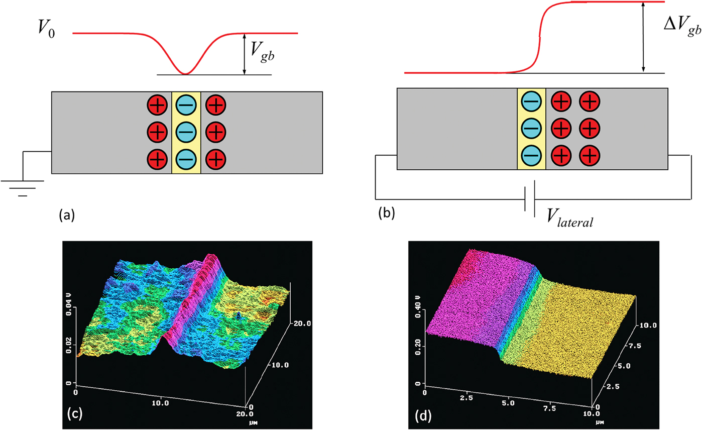
Figure 2: (a) On grounded surfaces, KPFM provides the information on static charge distributions due to the grain boundaries, dislocations, and composition variations. (b) On laterally biased devices, potential drops across the individual structural elements can be determined. Shown is the KPFM image of a (c) grounded and (d) laterally biased bicrystal of SrTiO3. Reprinted with permission from [Reference Kalinin and Bonnell33]. Copyright 2004 by the American Physical Society.

Figure 3: KPFM is extremely sensitive to the presence of surface contaminants that can screen internal potential distributions within a material. Shown is the evolution of surface potential of a SrTiO3 grain boundary. Note that while the lateral bias is applied, a clear potential drop across the GB is visible. This behavior is somewhat unexpected, since the resistive grain boundary in n-doped materials should be negatively charged, while positive feature is visible in Figure 2d. When the bias is turned off, the grain boundary shows negative contrast, which slowly relaxes with time. The explanation of the observed phenomena is the external screening at the grain boundary-surface junction, where on (b) equilibrated surface the grain boundary charge detected by KPFM is opposite to the intrinsic grain boundary charge. However, (c) temperature variation or application of lateral bias allows intrinsic GB charge to be observed. Reprinted with permission from [Reference Kalinin and Bonnell11]. Copyright 2004 American Chemical Society.
Lecture 3
The third lecture, “Dynamic KPFM modes,” introduces the complex excitation modes in KPFM. The need for these can be understood as the following. Even for ideal feedback and in the absence of environmental effects, the classical KPFM method is predicated on a number of assumptions, including that the electrostatic force is parabolic in bias (with the apex determined by surface potential and curvature given by capacitance) and the interaction is time-independent. Classical KPFM does not provide capacitance information. Furthermore, in the presence of mobile ionic charges or non-zero surface density of states (either electronic or ionic), electrostatic forces can become time-dependent and non-parabolic. This lecture introduces the viewer to the broad variety of KPFM modes enabled by multifrequency detection, band excitation, and G-Mode—all of which expand the materials characteristics and behaviors that can be detected by KPFM [Reference Collins12–Reference Collins14]. The lecture concludes with an introduction to G-Mode KPFM, capable of probing electrostatic phenomena with microsecond time resolution, and discusses future opportunities for this method.
Lecture 4
The fourth lecture in this series presents “Lateral transport measurements in KPFM.” The viewer is first introduced to basic principles of the method, where the moving SPM probe is used like a moving voltage electrode in four-probe measurements [Reference Tanimoto and Vatel15,Reference Vatel and Tanimoto16]. An example is shown of quantitative studies of Schottky and Zener diodes and grain boundary conductance in oxides (Figures 2 and 3). The role of environmental effects is also discussed [Reference Kalinin17]. The viewer is then introduced to time-resolved (tr) KPFM measurements (Figure 4) [Reference Strelcov18]. The KPFM measurements in the frequency domain, referred to as scanning impedance microscopy (SIM), and its nonlinear and frequency-mixing versions, are featured [Reference Shin19–Reference Kalinin21]. Finally, the applications of SPM for probing the field effect in carbon nanotubes, referred to as scanning gate microscopy (Figures 1b and 1c), are illustrated [Reference Freitag22].

Figure 4: Time-resolved (tr) KPFM of potential evolution across a lateral electrochemical device. Shown is the evolution of potential drop between the electrodes as a function of time. In the bias on state, the potential distribution is initially uniform and later develops the potential drop at the electrode due to electrochemical polarization. In the bias off state, the effect of the metastable screening charges can be clearly observed. Reprinted with permission from [Reference Strelcov18]. Copyright 2013 American Chemical Society.
Lecture 5
This lecture introduces “KPFM in liquid environments.” Understanding of corrosion, battery functionalities, and biological systems all necessitate probing of electrochemical behaviors in liquids. However, in this case the electrolyte itself is an active component of the imaging process, and the ionic and electrochemical processes in liquids can strongly affect the forces acting on the cantilever. The time dynamics of ionic phenomena in liquids, including electrode polarization and ionic transport, are analyzed. Electrochemical force microscopy (EcFM) is introduced as a technique to probe both time- and voltage-dynamics of bias-induced forces in liquids and is extended to spatially resolved imaging [Reference Collins23], giving rise to complex multidimensional data sets. Several approaches for visualization of resultant 4-D objects based on multivariate statistics are introduced.
Lecture 6
This lecture presents “I-V measurements in SPM.” Here, the detected signal is current flowing from the tip to the surface, similar to classical electrical characterization methods. The lecture introduces classical semiconductor characterization techniques, such as scanning spreading resistance microscopy and conductive AFM, as well as their generalization to frequency-dependent transport in nanoimpedance microscopy [Reference Shao24, Reference O'Hayre25]. Scanning potentiometry, multiple-probe SPM, and scanning capacitance microscopy (SCM) are further discussed. The lecture then introduces methods for SPM-based electrical nanofabrication, including nanooxidation, charge decoration, and local electrochemistry [Reference Lee26, Reference Garcia27]. More subtle bias-induced effects including bias-induced melting and superlubricity are discussed [Reference Strelcov28]. Finally, the viewer is introduced to (a taste of) big data applications in I-V measurements, including multivariate analysis of the I-V data and direct data mining of structure-function data, as exemplified by the scanning tunneling spectroscopy of superconductor materials [Reference Ziatdinov29, Reference Ziatdinov30].
Lecture 7
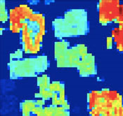
This final lecture, “Dynamic IV measurements,” introduces I-V techniques and spectroscopies for analysis of coupled electronic and ionic phenomena in complex materials. This lecture introduces the viewer to I-V measurements on mixed ion and electron conductive materials and describes electrochemical effects during I-V spectroscopies. The I-V-z spectroscopies are introduced as universal techniques to probe electrochemical reactions and explore the role of environmental effects on reactivity. Feedback-limited methods, including galvanostatic amplitude- and frequency-based techniques, are introduced for probing time-dependent electrochemical processes. The environmental effects and mechanisms of tip-induced reactions are discussed, as are general principles for electrochemically well-defined experiments. Subsequently, the viewer is introduced to multidimensional I-V spectroscopies, including first order reversal curve measurements. Machine learning methods including Bayesian linear unmixing are introduced to link these measurements to specific transport mechanisms (Figure 5). The extension of these methods to probe electrochemical phenomena on the atomic level [Reference Vasudevan31], as well as Bayesian-inference-based ultrafast spectroscopies [Reference Somnath32], are discussed.
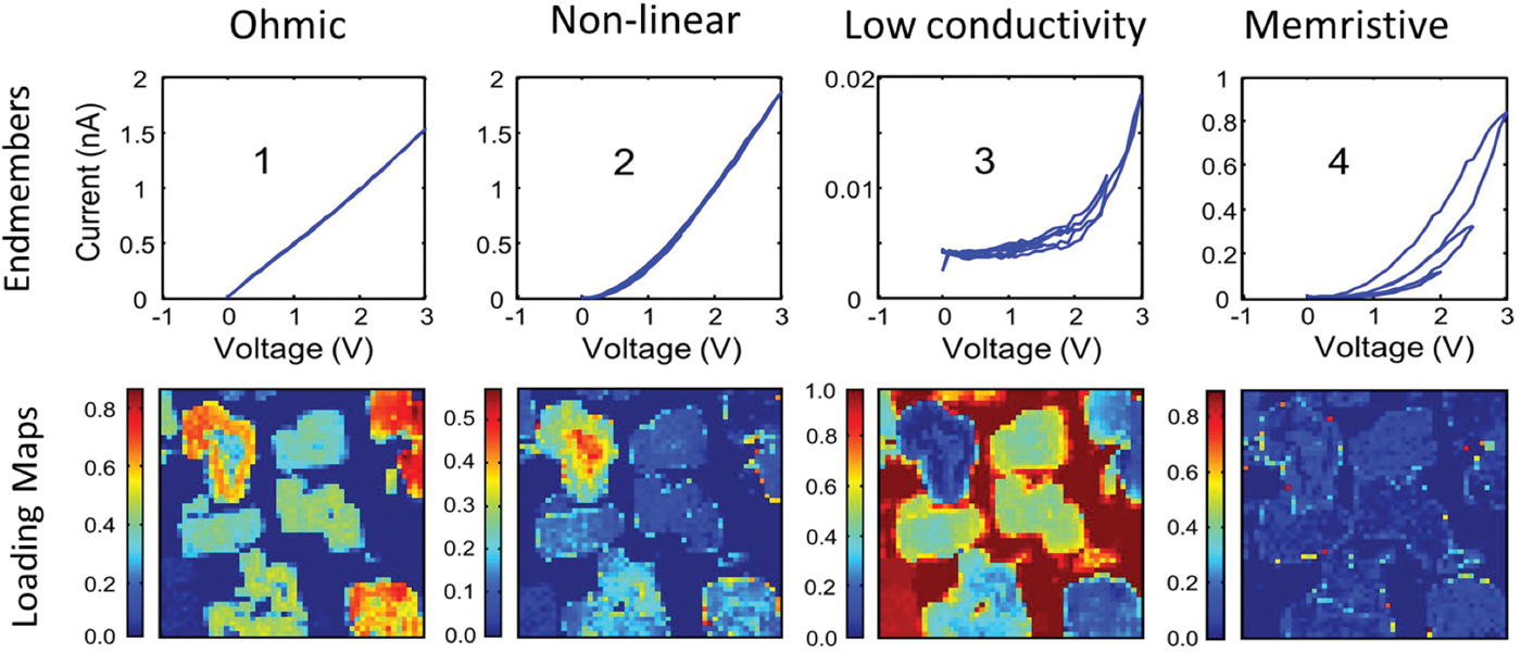
Figure 5: Multivariate analysis of the first order reversal curve in current-voltage mapping of the tubular spinel-perovskite interface. Application of Bayesian Linear Unmixing (BLU) to the 4-D data set allows separation of individual transport components that possess clear physical meaning. The first component (localized in parts of the grains) exhibits clear linear Ohmic form. The second component is non-linear, and is localized in the complementary regions of the grains. Interestingly, this behavior cannot be anticipated a priori. The third component represents the residual resistance of the non-conductive matrix. Finally, the fourth component shows clear hysteresis in the I-V curves and is localized exclusively at the interfaces. In this manner, multivariate analysis with physical constrains allows clear separation of materials-specific behaviors in the a priori unknown system. Reprinted with permission from [Reference Strelcov34]. Copyright 2014 American Chemical Society.
Overall, this lecture series includes ∼350 slides and 7 hours of narration. It introduces the viewer to modern SPM-based transport measurements, including principles and potential pitfalls, and provides additional references for those interested in further details or hands-on implementation.
Acknowledgments
The work was supported by the Center for Nanophase Materials Sciences, a U.S. Department of Energy, Office of Science User Facility at Oak Ridge National Laboratory.


