


1. Introduction
Nitrogen containing III-V-V' alloys, such as GaN(In)As and GaN(In)P have in recent years emerged as a subject of considerable theoretical and experimental research interest, due to their very unique physical properties and a wide range of possible device applications. Unlike all conventional ternary III-V semiconductor alloys, such as AlGaAs, GaInAs, GaInP, etc., where the band gap energy of the alloy can be reasonably approximated as a weighted linear average of the band gaps of the parental binary compounds, N-containing anion-mixed III-V alloys exhibit a huge bowing in the band gap energy Reference Weyers and Sato[1] Reference Weyers, Sato and Ando[2] Reference Sato[3] Reference Kondow, Uomi, Hosomi and Mozume[4] Reference Bi and Tu[5] Reference Uesugi and Suemune[6] Reference Sakai, Ueta and Terauchi[7] Reference Wei and Zunger[8] Reference Bellaiche, Wei and Zunger[9] Reference Bellaiche, Wei and Zunger[10] Reference Bellaiche, Wei and Zunger[11]. For example, the addition of only 2 % of nitrogen to GaAs causes a dramatic decrease in band gap energy by about 0.4 eV.
These remarkable fundamental properties of the GaN(In)As ternary and quaternary alloys, in combination with the possibility to vary the lattice constant of the alloy material in a wide range by optimizing the N content, provide an opportunity to tailor the material properties for desired applications in optoelectronic devices based on III-V materials. First of all, the incorporation of nitrogen has made possible to synthesize III-V compounds that are lattice matched to Si. For example, with 20% N incorporation into GaAs or 2% N in GaP, GaN0.2As0.8 or GaN0.02P0.98 can be lattice matched to Si. Thus a drastic improvement in the quality of III-V epitaxial films grown on Si substrates can be achieved, providing the possibility of integrating direct band gap III-V compounds with Si. This would fulfill a long-sought desire for fabrication of optoelectronic and photonic devices based on the most-developed and most-mature Si technology, which not only offers advantages of large-area substrates, large-scale and low-cost fabrication, but also opens the door for integration of microelectronic and optoelectronic devices on a chip.
On the other hand, GaInNAs alloys with a low nitrogen content can also be made lattice matched to GaAs or InP with a band gap anywhere between ~ 1.42 eV and 0.6 eV. Hence GaInNAs has recently been demonstrated Reference Kondow, Uomi, Niwa, Kitatani, Watahiki and Yazawa[12] Reference Kondow, Kitatani, Nakatsuka, Larson, Nakahara, Yazawa, Okai and Uomi[13] Reference Kondow, Kitani, Nakahara and Tanaka[14] Reference Miyamoto, Takeuchi, Koyama and Iga[15] Reference Sato and Satoh[16] Reference Borchert, Yu Egorov, Illek, Komainda and Riechert[17] Reference Fischer, Reinhardt and Forchel[18] as a new key material system for long wavelength lasers emitting at the optical-fiber communication wavelength window (1.3 - 1.55 μm) with a high temperature performance, as well as for multi-junction solar cells Reference Kurtz, Myers and Olson[19] Reference Friedman, Geisz, Kurtz and Olson[20] Reference Kurtz, Allerman, Jones, Gee, Banas and Hammons[21] (photovoltaics) with high efficiency. For laser applications this new material system has several important advantages as compared with the commonly used InGaAs/InGaAsP and InGaAsP/InP systems. First of all, a better high-temperature performance of the laser structures is achieved due to a larger conduction band offset and, thus, improved electron confinement. Secondly, the increase of the electron effective mass with the addition of nitrogen provides a close match between the effective mass values for electrons and holes, beneficial for laser applications. Moreover, the possibility to grow coherently GaInNAs on GaAs enables fabrication of vertical-cavity surface-emitting lasers (VCSELs) based on the high refractive index contrast AlGaAs/GaAs Bragg reflectors. In case of the photovoltaics, the addition of GaInNAs cells to a commercial tandem InGaP-GaAs structure can improve the internal quantum efficiency to a record value of ~ 70 % Reference Kurtz, Allerman, Jones, Gee, Banas and Hammons[21], due to the collection by GaInNAs cells of the longer wavelength ( > 850 nm) infrared light, which passes unabsorbed through both the InGaP and GaAs cells.
In this paper we attempt to give a brief review on the present knowledge of the electronic properties of the Ga(In)NAs materials, mainly from an experimental perspective. The discussion will be focused on GaNxAs1−x and GaInNxAs1−x alloys with low N composition (x< 10 %), to which a large amount of experimental work has been devoted over the past years. Incorporation of higher N content, unfortunately, causes severe degradation of the alloy quality resulting in the formation of highly inhomogeneous material with inclusions of GaN, GaNAs and GaAs phases Reference Foxon, Cheng and Novikov[22]. The same applies to the GaN-rich side of GaNAs, where severe phase separation occurs with As composition as low as 0.005 Reference Kuroiwa, Asahi, Asami, Kim, Iwata and Gonda[23]. This is because of an extremely large miscibility gap between GaN and GaAs caused by the large differences in lattice constant and in lattice structure (GaN: wurtzite, GaAs: zincblende).
The paper is organized as follows. We shall first discuss the nature of the giant band gap bowing in the alloy, which is by far the most interesting property of the material. Since the bowing mainly occurs in the conduction band (CB), the emphasis will be on nitrogen-induced modification of the CB states revealed by various experiments. The current knowledge on the other key material parameters relevant for the device applications, such as electron effective mass and band alignment in the Ga(In)NAs/GaAs heterostructures, will also be reviewed. Since the main motivation for the alloy fabrication is to improve the performance of optoelectronic devices, the second part of the paper will deal with recombination processes in Ga(In)NAs. The bulk of the discussion will be related to radiative recombination processes in the material, which are relatively well understood. The brief outlook of the much less known non-radiative recombination processes will be given in the final part of the paper.
2. Fundamental band structure properties
2.1 Giant bowing of the bandgap energy
The success in fabrication of the high quality III-V alloys based on the (Al, Ga, In)(As,P) material system, as well as the breakthrough in the growth of III-Nitrides in the early 90th has encouraged the growth of III-V-N alloys with the motivation to close the gap between the nitrides and the arsenides, and thus to fabricate light emitters covering the entire visible spectral range based on the direct band-gap III-V materials. From early absorption measurements Reference Weyers, Sato and Ando[2] Reference Sato[3] Reference Kondow, Uomi, Hosomi and Mozume[4] Reference Bi and Tu[5], the GaNxAs1−x alloy has indeed been proven to have a direct band-gap. However, instead of the expected blue shift from the GaAs bandgap, the GaNAs alloy has shown a considerable red shiftin absorption Reference Weyers, Sato and Ando[2] Reference Sato[3] Reference Kondow, Uomi, Hosomi and Mozume[4] Reference Bi and Tu[5] Reference Uesugi and Suemune[6] Reference Pozina, Ivanov, Monemar, Thordson and Andersson[24] Reference Uesugi, Morooka and Suemune[25] and photoluminescence (PL) near the band edge Reference Weyers, Sato and Ando[2] Reference Francoeur, Sivaraman, Qiu, Nikishin and Temkin[26] Reference Buyanova, Chen, Pozina, Bergman, Monemar, Xin and Tu[27] Reference Gruning, Chen, Hartmann, Klar, Heimbrodt, Höhnsdorf, Koch and Stolz[28], suggesting a decrease in the bandgap energy with increasing N composition- see .
The deviation of the bandgap energy from the composition weighted linear average of the band-gaps of the parental binary compounds forming the alloy is usually described by a correction term
where the bowing coefficient b is typically a fraction of an eV and is composition independent. However, in contrast to the conventional III-V alloys, the optical bowing coefficient in III-V-N is huge, i.e. of the order of 18 - 20 eV for x < 5%, and strongly depends on N content (). Moreover, the rather different compositional dependence of the GaNAs band gap measured for layers grown on GaAs or GaP substrates, respectively (Figure 1), implies that the bowing coefficient should also depend on the internal strain in the GaNAs epilayer. The strain is created due to the lattice mismatch with the substrate material Reference Uesugi, Morooka and Suemune[25]. Strain relaxation in the rather thick (≈ 2 μm) GaNAs layers, commonly used for the absorption measurements, can also explain the very abrupt change in the slope of the compositional dependence of the bandgap energy observed in experiments at around x ≈ 3 − 4 %.

Figure 1. Compositional dependence of the band gap energy of GaNxAs1−x. The points represent experimental data, corrected to room temperature. The lines show results of theoretical calculations. The legend indicates references and the measurements or theoretical approaches used. The bowing coefficient deduced by the dielectric model calculations (the blue dotted line) is 20 eV.
The first theoretical explanation of the observed strong reduction in the bandgap energy has been provided Reference Sakai, Ueta and Terauchi[7] within the Van Vechten model (shown by the blue dashed line in Figure 1). The large electronegativity of N atoms has been shown to cause bowing in the conduction band (CB) energy of the alloy with a bowing coefficient of 20 eV. This dielectric model provides very good agreement with the experimental results for the lowest nitrogen compositions, i.e. x < 2% (Figure 1). However, it predicts a negative bandgap for GaNAs in most of the composition range, i.e. 9.5-86.7%, based on a constant value of the bowing coefficient.
This prediction has been disproved by later experiments Reference Bi and Tu[5] Reference Uesugi and Suemune[6], where a clear reduction of the bowing coefficient with increasing N content leads to discrepancy between the theoretical predictions and the experimentally determined values of the bandgap energy for the alloys with x > 2% - Figure 1. The reduction of the bowing coefficient has been explained by the first-principle local-density approximation (LDA) calculations of the band structure Reference Wei and Zunger[8] Reference Bellaiche, Wei and Zunger[9] Reference Bellaiche, Wei and Zunger[10] Reference Bellaiche, Wei and Zunger[11]. Based on analysis of the highly localized nature of the perturbations introduced by N atoms due to a large chemical and size difference between N and the other column V anions it replaces, two regions in the bandgap variation of the III-V-N alloys has been predicted. An impurity-like region with a large and compositional dependent bowing coefficient is expected for the low N compositions up to 10%, whereas a band-like region with a much smaller and nearly constant bowing coefficient is predicted for the intermediate compositions x = 10 − 40 % Reference Wei and Zunger[8]. The results of the first principle calculations for bulk GaNAs are shown in Figure 1 by the red curve, and are in reasonable agreement with the experimental data for large (> 5%) nitrogen compositions. By considering the effect of the residual strain on the alloy properties Reference Bellaiche, Wei and Zunger[10], better agreement between the LDA theory and the experiments can be achieved (the results of the LDA calculations for strained GaNAs/GaAs and GaNAs/GaP structures are shown in Figure 1 by black and green lines, respectively).
2.2 Conduction band states : Nitrogen-activated E- and E+ levels
Further insight on the nature of band states in III-(III')-V-N alloys has been gained after the discovery of the additional feature (denoted as E+) in the electro- Reference Perkins, Mascarenhas, Zhang, Geisz, Friedman, Olson and Kurtz[29] and photoreflectance Reference Shan, Walukiewicz, Ager, Haller, Geisz, Friedman, Olson and Kurtz[30] Reference Shan, Walukiewicz, Ager, Haller, Geisz, Friedman, Olson and Kurtz[31] Reference Walukiewicz, Shan, Ager, Chamberlin, Haller, Geisz, Friedman, Olson and Kurtz[32] spectra of Ga(In)NxAs1−xalloys with x > 1%, and the observation of the unusual pressure dependence of the alloy band gap Reference Shan, Walukiewicz, Ager, Haller, Geisz, Friedman, Olson and Kurtz[30] Reference Shan, Walukiewicz, Ager, Haller, Geisz, Friedman, Olson and Kurtz[31] Reference Walukiewicz, Shan, Ager, Chamberlin, Haller, Geisz, Friedman, Olson and Kurtz[32] Reference Jones, Modine, Allerman, Kurtz, Wright, Torez and Wei[33] Reference Jones, Modine, Allerman, Fritz, Kurtz, Wright, Torez and Wei[34] Reference Jones, Allerman, Kurtz, Modine, Bajaj, Torez and Wei[35].
A typical electroreflectance (ER) spectrum measured from a thick GaNAs epilayer is shown in Figure 2. Three fundamental transitions are clearly seen: (i) the band gap transition (denoted as either Eo Reference Perkins, Mascarenhas, Zhang, Geisz, Friedman, Olson and Kurtz[29] or E− Reference Shan, Walukiewicz, Ager, Haller, Geisz, Friedman, Olson and Kurtz[30] Reference Shan, Walukiewicz, Ager, Haller, Geisz, Friedman, Olson and Kurtz[31] Reference Walukiewicz, Shan, Ager, Chamberlin, Haller, Geisz, Friedman, Olson and Kurtz[32]); (ii) the transitions from the spin-orbit split-off valence band (E0 + Δ0), which are intrinsic to all zinc blende III-V semiconductors; (iii) an additional third feature (E+), which appears in the spectra of the GaNxAs1−x samples with x > 0.8% and in GaInNAs samples with x ≥ 1.2%. The evolution of the ER spectra as a function of N composition is demonstrated in Figure 3.

Figure 2. Electroreflectance spectra at RT for a 2 μm thick GaAsN film on a GaAs substrate. The band gap transition (E0) at 1.19 eV as well as the transition from the spin-orbit split-off VB (E0+Δ0) at 1.52 eV are easily seen. An additional weak feature (E+) at 1.83 eV is more clearly seen in the second spectrum at 10x and offset for clarity. The fitted line shape for the E0+Δ0 and E+ transitions are shown with dashed lines and offset for clarity. (After Ref. Reference Perkins, Mascarenhas, Zhang, Geisz, Friedman, Olson and Kurtz[29])

Figure 3. Electroreflectance spectra at RT for thick GaAsN (a)-(h) and GaInNAs [(i) and (j)] films grown on a GaAs substrate. For GaNAs samples, the nitrogen composition ranges from x=0 (a) to x=2.8 % (h). For GaInAsN samples, the compositions are Ga0.95In0.05As0.987N0.013 (i) and Ga0.92In0.08As0.978N0.022(j). (After Ref. Reference Perkins, Mascarenhas, Zhang, Geisz, Friedman, Olson and Kurtz[29])
The reflectance measurements Reference Perkins, Mascarenhas, Zhang, Geisz, Friedman, Olson and Kurtz[29] Reference Shan, Walukiewicz, Ager, Haller, Geisz, Friedman, Olson and Kurtz[30] Reference Shan, Walukiewicz, Ager, Haller, Geisz, Friedman, Olson and Kurtz[31] Reference Walukiewicz, Shan, Ager, Chamberlin, Haller, Geisz, Friedman, Olson and Kurtz[32] provided very valuable information on the electronic structure of the Ga(In)NAs. First of all, the independence of the spin-orbit splitting Δ0on N concentration in the material (Figure 3) gives a direct experimental evidence for a negligible effect of N on the electronic structure of the valence band (VB) states in the alloy. Moreover, it also proves that the E+ level represents an upper lying subband of the conduction band.
The following properties of the E− and E+ levels have been revealed, and are important to clarify the nature of the CB band states.
2.2.1. Dependence on nitrogen composition
With increasing nitrogen content in the alloy the spectral position of the E− transitions shifts towards lower energies - Figure 3, representing the giant band gap bowing effect discussed above. On the contrary, the E+ transition shifts Reference Perkins, Mascarenhas, Zhang, Geisz, Friedman, Olson and Kurtz[29] Reference Shan, Walukiewicz, Ager, Haller, Geisz, Friedman, Olson and Kurtz[30] Reference Shan, Walukiewicz, Ager, Haller, Geisz, Friedman, Olson and Kurtz[31] Reference Walukiewicz, Shan, Ager, Chamberlin, Haller, Geisz, Friedman, Olson and Kurtz[32] towards higher energies with increasing x, and its intensity increases relative to the E− intensity (Figure 3). From the observed linear dependence of the E+-E− splitting vs nitrogen composition (Figure 4), the energy position of the E+ level in GaAs has been extrapolated to Ev+1.68 eV Reference Perkins, Mascarenhas, Zhang, Geisz, Friedman, Olson and Kurtz[29]. Based on the energy position, the E+level could be attributed either to the nitrogen level EN resonant with the CB, known to have energy level at 1.65-1.70 eV above the VB Reference Hjalmarson, Vogl, Wolford and Dow[36] Reference Wolford, Bradley, Fry, Thompson, Chadi and Harrison[37], or a higher lying L-minimum of the CB at Ev+1.71 eV.

Figure 4. Compositional dependence of the E− and E+ transition energies. The points represent the experimental data. The lines are a guide to the eye. The legend indicates the references.
2.2.2. Pressure dependence
In sharp contrast to the parent Ga(In)As material, where the fundamental bandgap energy increases linearly under applied hydrostatic pressure, the bandgap energy in the N-containing alloys (corresponding to the E-transitions) exhibits a much weaker sublinear pressure dependence with a tendency to saturate at high pressures. The unusual pressure behavior of the bandgap energy has been detected both via photoreflectance Reference Shan, Walukiewicz, Ager, Haller, Geisz, Friedman, Olson and Kurtz[30] Reference Shan, Walukiewicz, Ager, Haller, Geisz, Friedman, Olson and Kurtz[31] Reference Walukiewicz, Shan, Ager, Chamberlin, Haller, Geisz, Friedman, Olson and Kurtz[32] and photoluminescence Reference Jones, Modine, Allerman, Kurtz, Wright, Torez and Wei[33] Reference Jones, Modine, Allerman, Fritz, Kurtz, Wright, Torez and Wei[34] Reference Jones, Allerman, Kurtz, Modine, Bajaj, Torez and Wei[35] measurements (some representative experimental data for GaNAs and GaInNAs are shown in Figure 5a and Figure 5b, respectively). On the other hand, pressure dependence of the E+ transition undergoes a change opposite to E−, i.e. the E+ energy position weakly depends on the applied pressure at low pressures and demonstrates much stronger linear increase at high pressures - Figure 5a and Figure 5b. This implies a pressure-induced change in the character of the E+ subband, consistent with the observed strong increase in the intensity of the E+ transitions at high pressure Reference Shan, Walukiewicz, Ager, Haller, Geisz, Friedman, Olson and Kurtz[30] Reference Shan, Walukiewicz, Ager, Haller, Geisz, Friedman, Olson and Kurtz[31].

Figure 5a. Effects of hydrostatic pressure on the energies of the E− and E+ transitions in GaNAs. The blue triangles represent the RT photoreflectance (PR) data Reference Shan, Walukiewicz, Ager, Haller, Geisz, Friedman, Olson and Kurtz[31] for a GaNAs epitaxial layer with %N=1.5%. The blue lines are results from the BA calculations for the same structure Reference Shan, Walukiewicz, Ager, Haller, Geisz, Friedman, Olson and Kurtz[31]. The dashed and dashed-dotted lines represent the pressure dependencies of the Γ CB edge (EΓ) of GaAs and N-related level (EN), respectively. The red lines show results of the LDA calculations Reference Mattila, Wei and Zunger[42] for GaNAs with %N=0.8%.

Figure 5b. Effects of hydrostatic pressure on the energies of the E− and E+ transitions in GaInNAs. The blue triangles represent the RT photoreflectance data Reference Shan, Walukiewicz, Ager, Haller, Geisz, Friedman, Olson and Kurtz[30] obtained for a GaInNAs epitaxial layer with %In = 5% and %N=1.2%. The blue lines show results from the BA calculations for the same structure Reference Shan, Walukiewicz, Ager, Haller, Geisz, Friedman, Olson and Kurtz[30], assuming a linear pressure dependence of the Γ CB edge (~100 meV/GPa) and the N-related level (~15 meV/GPa), shown by dashed-dotted lines. The red dots show the PL data from Ref. 33 for a thick lattice-matched GaInNAs epilayer with %In = 7% and %N= 2%, for comparison. The red line represents the results of the LDA calculations Reference Jones, Modine, Allerman, Kurtz, Wright, Torez and Wei[33] for the same structure, which are offset by 1.14 eV to achieve the agreement with the experiment at ambient pressure.
All aforementioned experimental observations provided direct evidence that the nitrogen-induced interaction between the E− and E+ levels causes the reduction of the alloy bandgap. However, the physical origin of this interaction remains a subject of ongoing debate. Two main models, which imply rather different character of the conduction band states, are currently discussed:
-
1. The empirical band-anticrossing (BA) model Reference Shan, Walukiewicz, Ager, Haller, Geisz, Friedman, Olson and Kurtz[30] Reference Shan, Walukiewicz, Ager, Haller, Geisz, Friedman, Olson and Kurtz[31] Reference Walukiewicz, Shan, Ager, Chamberlin, Haller, Geisz, Friedman, Olson and Kurtz[32] assumes that the CB splitting into the E− and E+ subbands is a result of interaction between the delocalised Γ minimum of the CB and the nitrogen-related level EN, EN= Ev+1.65 eV - Figure 6. The strength of the Γ − EN interaction is described by the interband matrix element VMN. (As additional fitting parameters, the interactions between EN and the higher lying X- and L-minima can also be added Reference Gil[38]). According to this model, the E− subband has mainly delocalized CB –like character, whereas the E+ subband is due to the localized EN-like states. An increase in the VMN value with increasing N content leads to a stronger repulsion between the E− and E+ states and thus the band gap bowing accompanied with blue shift of the E+ state, as observed in the experiments – Figure 4. The unusual pressure dependence of the E− and E+ states is attributed to the pressure-induced band anticrossing, changing the character of the states from extended (localized) to localized (extended) ones - Figure 5a and Figure 5b. Due to the Γ - EN interaction, an increase of the electron effective mass me* and a strong non-parabolicity of the CB have also been predicted – see Figure 6.
-
Theoretical support for the band-anticrossing model has been provided by the sp3s* tight-binding calculations Reference Lindsay and O’Reilly[39] Reference Lindsay and O’Reilly[40] Reference Lindsay and O’Reilly[41]. The interband matrix element VMN has been found to increase as
with nitrogen composition x, where β is a constant dependent on the semiconductor matrix. Using k · p theory, both conduction band dispersion and the compositional dependence of the effective mass value have been calculated Reference Lindsay and O’Reilly[39].
-
2. On the other hand, according to the uncorrected Reference Jones, Modine, Allerman, Kurtz, Wright, Torez and Wei[33] Reference Jones, Modine, Allerman, Fritz, Kurtz, Wright, Torez and Wei[34] and corrected Reference Mattila, Wei and Zunger[42] pseudopotential LDA calculations the formation of the E− and E+ levels is predominantly a result of a N-induced strong perturbation of the host crystal states leading to symmetry breaking. Due to the reduction of the crystal symmetry, the degenerate L and X minima split into a1 and t2 states. Mixing between the a1(Γ) and a1(L) conduction band states is responsible for the E− subband formation at ambient pressure. (The interaction between the CB states and the resonant EN level with a1 symmetry is suggested to have only a minor contribution to the E− formation Reference Mattila, Wei and Zunger[42]). The Γ-L interaction increases with increasing N composition leading to an increasing contribution of the L character with increasing x, i.e. up to 20 % for N=0.8%. On the other hand the mixing with the X- states prevails under applied pressure, leading to the experimentally observed reduction of pressure coefficient for the E− states at high pressures- Figure 5a and Figure 5b. The increasing admixing of the E− states with the L (X) states (with heavier electron effective masses) will also cause an increase of me* value with x (or pressure). In contrast to the band anticrossing model, the E− states in the Ga(In)NAs alloys are suggested Reference Mattila, Wei and Zunger[42] to be localized in real space, which causes a decrease of electron mobility. The E+ states are deduced Reference Mattila, Wei and Zunger[42] to originate from a weighted average of the a1(N) and a1(L) levels based on their Γ character. With increasing N content, the E+ level has been found to increase linearly with energy with a slope nearly equal to the decrease in E−

Figure 6. Schematic of dispersion relations for the E− and E+ subbands based on the band anticrossing model Reference Walukiewicz, Shan, Ager, Chamberlin, Haller, Geisz, Friedman, Olson and Kurtz[32]. The unperturbed energies of the N-related level (EN) and the GaAs conduction band (EΓ) are also shown.
Both models provide good qualitative agreement with experimental data and can account for the compositional and pressure dependencies of the E+ and E− levels. As an example, Figure 5a and Figure 5b compare the experimentally determined pressure dependence of the E+ and E− transitions in GaNAs and GaInNAs, respectively, with the results of theoretical calculations using the band anticrossing model Reference Shan, Walukiewicz, Ager, Haller, Geisz, Friedman, Olson and Kurtz[30] Reference Shan, Walukiewicz, Ager, Haller, Geisz, Friedman, Olson and Kurtz[31] Reference Walukiewicz, Shan, Ager, Chamberlin, Haller, Geisz, Friedman, Olson and Kurtz[32] and the LDA approach Reference Jones, Modine, Allerman, Kurtz, Wright, Torez and Wei[33] Reference Jones, Modine, Allerman, Fritz, Kurtz, Wright, Torez and Wei[34] Reference Mattila, Wei and Zunger[42]. Both models can also qualitatively describe the experimentally observed increase of the electron effective mass in the alloys with increasing N composition/pressure (to be discussed below).
In order to ascertain the nature of the band gap bowing in the alloys, several experiments probing the nature of the E+ and E− levels have been reported recently. Ballistic electron emission microscopy (BEEM) studies suggest that the E+ level has predominantly L-like character Reference Kozhevnikov, Narayanamurti, Reddy, Xin, Tu, Mascarenhas and Zhang[43]. A similar conclusion has been reached from resonant Raman scattering studies, based on the observed activation of the L-point phonons in resonance with the E+ states Reference Cheong, Zhang, Mascarenhas and Geisz[44]. Both observations have been considered as favoring the LDA approach.
On the other hand, the suppression of the temperature dependence of the bandgap energy in GaNAs Reference Uesugi, Suemune, Hasegawe and Akutagawa[45] and GaInNAs Reference Polimeni, Cappizzi, Geddo, Fischer, Reinhardt and Forchel[46] alloys as compared with GaAs seems to be more consistent with the band-anticrossing model. This is because the admixture of the L-states with stronger temperature dependence into E− should enhance the temperature dependence of the bandgap energy, opposite to experimental findings – Figure 7.

Figure 7. Temperature dependent shift of the band gap energy detected via (a) absorption in the GaNAs/GaAs epilayers, according to Ref. Reference Uesugi, Suemune, Hasegawe and Akutagawa[45], and (b) via photoluminescence in GaInNAs/GaAs single QW structures, according to Ref. Reference Polimeni, Cappizzi, Geddo, Fischer, Reinhardt and Forchel[46].
Attempts have also been undertaken to study directly the N-induced modifications of the L-states by monitoring the E1 transitions near the L-point of the Brillouin zone Reference Gruning, Chen, Hartmann, Klar, Heimbrodt, Höhnsdorf, Koch and Stolz[28] Reference Shan, Walukiewicz, Yu, Ager, Haller, Geisz, Friedman, Olson, Kurtz and Nauka[47] Reference Leibiger, Gottschalch, Rheinländer, Sik and Schubert[48]. Only a minor N-induced increase of the E1 energy has been detected – Figure 8, proving a weak effect of N on the higher lying L minimum. The failure to observe the LDA-predicted splitting of the L- states into a1 (L) and t2(L) components, as well as a small red shift of the E1 transitions with increasing x (i. e. opposite to the trend expected for the lower a1(L) component Reference Mattila, Wei and Zunger[42]) have led to the conclusion Reference Shan, Walukiewicz, Yu, Ager, Haller, Geisz, Friedman, Olson, Kurtz and Nauka[47] that the Γ - L (X) interactions do not contribute significantly to the band formation in the alloy. Further investigations are needed to clarify the issue.

Figure 8. Change in the energy position of the E1 transition as a function of N composition.
2.3 Conduction band dispersion. Electron effective mass
As has been discussed above, the electron effective mass me* in III-(III')-V-N has been predicted Reference Walukiewicz, Shan, Ager, Chamberlin, Haller, Geisz, Friedman, Olson and Kurtz[32] Reference Jones, Modine, Allerman, Kurtz, Wright, Torez and Wei[33] Reference Jones, Modine, Allerman, Fritz, Kurtz, Wright, Torez and Wei[34] Reference Lindsay and O’Reilly[39] Reference Mattila, Wei and Zunger[42] to increase with increasing N composition x in the low composition range. This behavior is rather unusual and in fact is opposite to the conventional semiconductors, where the value of the effective mass decreases with decrease of bandgap energy. Moreover, the conduction band in the alloys is predicted to be very non-parabolic Reference Walukiewicz, Shan, Ager, Chamberlin, Haller, Geisz, Friedman, Olson and Kurtz[32] Reference Lindsay and O’Reilly[39], leading to a strong energy dependence of the effective mass.
2.3.1. Effective mass at ambient pressure
The knowledge of the carrier effective masses at ambient pressure provides valuable information on the fundamental nature of the band states in the alloy and is also vitally important for a full exploration and optimization of the III-(III')-V-N alloys in device applications. The first experimental values for the electron effective mass in GaNAs and GaInNAs alloys have been obtained only very recently Reference Hai, Chen, Buyanova, Xin and Tu[49] Reference Skierbiszewski, Perlin, Wisniewski, Knap, Suski, Walukiewicz, Shan, Yu, Ager, Haller, Geisz and Olson[50].
auto The GaNAs alloy
For GaNAs/GaAs quantum well (QW) structures the compositional dependence of the electron effective mass me has directly been determined by using optically detected cyclotron resonance (ODCR) measurements Reference Hai, Chen, Buyanova, Xin and Tu[49]. Since the position of the ODCR maximum is directly related to the carrier effective mass value and the width of the resonance reflects the carrier scattering time in the material, both parameters can be simultaneously determined by analyzing the lineshape of the ODCR peak. By tuning the laser photon energy between the band gaps of GaAs and the GaNAs QWs, the ODCR signal related to the GaAs electrons could be avoided to provide access to the electrons confined in the GaNAs QWs. Based on the clear compositional dependence of the ODCR maximum position measured under such resonant excitation of the GaNAs - Figure 9, the electron effective mass has been found to increase up to 0.19 m0 with N= 2%. A strong broadening of the ODCR spectra with x provides evidence for at least 50% decrease in scattering time in the GaN0.02As0.98 alloy as compared with GaAs. Thus both effects, i.e. increase of the electron effective mass value and the decrease in the scattering time have been concluded to contribute to a decrease of the electron mobility in GaNAs.

Figure 9. (a) The ODCR spectrum arising from the GaAs layers (x=0) in the GaAsN/GaAs QWs structures when the excitation energy was tuned above the GaAs bandgap. (b)-(c) The ODCR spectra of the GaAsN QWs, when the excitation photon energy was tuned at 1.475 eV, i.e. below the GaAs bandgap but above the bandgap of the GaAsN QWs. The dashed lines represent experimental data. The solid lines are the fit curves Reference Hai, Chen, Buyanova, Xin and Tu[49] Reference Buyanova, Pozina, Hai, Chen, Xin and Tu[58] by using effective mass values specified in the Figure.
The observed trend of an increasing mass value with increasing N composition over the studied composition range is in agreement with earlier theoretical predictions Reference Walukiewicz, Shan, Ager, Chamberlin, Haller, Geisz, Friedman, Olson and Kurtz[32] Reference Jones, Modine, Allerman, Kurtz, Wright, Torez and Wei[33] Reference Lindsay and O’Reilly[39] Reference Mattila, Wei and Zunger[42]. The determined values, however, are somewhat higher than that expected from the band anticrossing model. For example, the experimentally determined electron effective is 0.19 mo for x = 0.02, whereas that from theory is below 0.11 m0 – Figure 10. Unfortunately, we can not compare our results with the LDA calculation, due to the lack, to the best of our knowledge, of the numerical theoretical data for GaNAs. We need to point out, however, that the measured compositional dependence of me strongly contradicts the conclusions of Ref. Reference Zhang, Mascarenhas, Xin and Tu[51], in which the opposite trend, i.e. a decrease of the me value with increasing x (for x > 1%), was deduced, based on indirect analysis of the quantum confinement effects (shown by open triangles in Figure 10). The inaccuracy of the latter analysis is not surprising, since the values of the other adjustable parameters, i.e. the hole effective mass in the GaNAs QWs, the conduction and valence band offset values, as well as their compositional dependence are currently unknown. Moreover, even the band alignment in this material system (i.e. type I or type II) is still under debate (to be discussed below). This will unavoidably lead to the large uncertainty in conclusions. In fact, the electron effective mass of 0.11 m0 for x= 1.6% has most recently been concluded from the analysis of very similar experimental data Reference Wu, Shan, Walukiewicz, Yu, Ager, Haller, Xin and Tu[52].
auto The GaInNAs alloy

Figure 10. Compositional dependence of the electron effective mass in the GaNAs alloy. The red dots represent experimentally determined values in GaNAs/GaAs QWs via the ODCR measurements Reference Hai, Chen, Buyanova, Xin and Tu[49]. The open triangles represent the values indirectly deduced by analyzing the quantum confinement energies in the GaNAs/GaAs QWs, from Ref. Reference Zhang, Mascarenhas, Xin and Tu[51]. The solid blue lines show predictions based on the BA model Reference Skierbiszewski, Perlin, Wisniewski, Suski, Walukiewicz, Shan, Ager, Haller, Geisz, Friedman, Olson and Kurtz[53]. The dashed green lines represent the results of the k · p calculations Reference Lindsay and O’Reilly[39].
The first experimental evidence on the unusual behavior of the electron effective mass in GaInNAs has been obtained from indirect optical measurements Reference Jones, Modine, Allerman, Kurtz, Wright, Torez and Wei[33] Reference Jones, Modine, Allerman, Fritz, Kurtz, Wright, Torez and Wei[34], due to the low carrier mobility of GaInNAs Reference Jones, Modine, Allerman, Fritz, Kurtz, Wright, Torez and Wei[34]. By using several methods such an analysis of exciton diamagnetic shift and quantum confinement energies in two-dimensional QW systems, the reduced exciton mass μ for 2% nitrogen was determined as μ = (0.13 – 0.2)mo.This value is 2 to 3 times heavier than that in GaAs. Assuming a negligible effect of nitrogen on the VB structure, a strong N-induced reduction of electron effective mass has been concluded. The effect has been attributed to the strong Γ-L and Γ-X mixing and quantitatively analyzed by using the LDA calculations, providing good agreement with the experimental data.
Direct measurements of the CB dispersion in GaInNAs have been performed very recently using infrared reflection Reference Skierbiszewski, Perlin, Wisniewski, Knap, Suski, Walukiewicz, Shan, Yu, Ager, Haller, Geisz and Olson[50]. The electron effective mass, determined at the Fermi energy, has been obtained from the onset energy of plasma reflection – Figure 11. An increase of the electron effective mass with the addition of nitrogen and, even more severe, with electron concentration, has been found in heavily Se-doped GaInNAs alloys, i.e. up to 0.4 m0 for In0.08Ga0.92As0.967N0.033with electron concentration of 6 × 10 19 cm−3- see Figure12. The observed strong dependence of the effective mass on carrier concentration provides the first direct evidence for an enhanced non-parabolicity of the conduction band in the alloy, and have been interpreted by the authors in terms of the band anticrossing model. The obtained values of the effective mass are comparable with earlier results [33, 34].
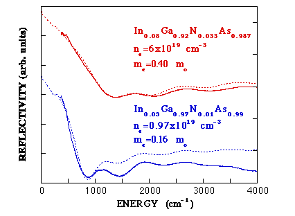
Figure 11. Experimental reflectivity spectra (solid lines) for two InGaNAs:Se samples with distinctly different electron concentrations. The dashed lines show fit Reference Skierbiszewski, Perlin, Wisniewski, Knap, Suski, Walukiewicz, Shan, Yu, Ager, Haller, Geisz and Olson[50] with indicated effective mass values (Courtesy C. Skierbiszewski).

Figure 12. Dependence of the measured electron effective mass on the electron concentration. The dots are experimental data Reference Skierbiszewski, Perlin, Wisniewski, Knap, Suski, Walukiewicz, Shan, Yu, Ager, Haller, Geisz and Olson[50]. The lines are a guide for the eye.
2.3.2. Effect of hydrostatic pressure
The dependence of electron effective mass on applied hydrostatic pressure has mainly been studied with an ambition to determine the origin of the level repulsion in the alloy. A clear qualitative trend of the strong pressure-induced enhancement in the electron effective mass induced by the presence of nitrogen in the alloy has been demonstrated. For GaNAs epilayers effect has been observed via a pressure-induced decrease in electron mobility, and interpreted within the BA model Reference Skierbiszewski, Perlin, Wisniewski, Suski, Walukiewicz, Shan, Ager, Haller, Geisz, Friedman, Olson and Kurtz[53]. For InGaAsN QW structures a pressure-induced enhancement of the electron effective mass is evident from the decrease of the exciton diamagnetic shift under applied pressure Reference Jones, Modine, Allerman, Fritz, Kurtz, Wright, Torez and Wei[34], and a pressure-induced broadening of the PL linewidth Reference Jones, Allerman, Kurtz, Modine, Bajaj, Torez and Wei[35]. The effect has been explained within the LDA approach. However, since both theoretical approaches predict similar qualitative pressure behavior of the electron effective mass, these experiments failed to single out the definite nature of the CB states.
2.4 Band alignment in Ga(In)NAs/GaAs heterostructures
The great potential for applications of the Ga(In)NAs alloy system for a range of optoelectronic and photonic devices can not be realized without detailed knowledge of the fundamental physical parameters related to the corresponding heterostructures, such as band alignment in the quantum structures and band offsets values. Moreover, the information about band alignment is also valuable in examining the validity of the approximations made in theoretical models, and thus the understanding of the fundamental band structure of the nitrogen containing III-V-N alloys.
2.4.1. GaNAs/GaAs structures
One of the remaining unsolved issues regarding the electronic properties of the GaNAs/GaAs quantum structures involves the band edge alignment. Although it is commonly accepted that the addition of nitrogen to GaAs mainly affects the CB states leading to a large CB offset and only a small VB discontinuity Reference Kozhevnikov, Narayanamurti, Reddy, Xin, Tu, Mascarenhas and Zhang[43] Reference Kitani, Kondow, Kikawa, Yazawa, Okai and Uomi[54], an in-depth understanding has so far been lacking, even about whether the fundamental type of the band alignment is type I or type II. Early theoretical studies using the dielectric model Reference Sakai, Ueta and Terauchi[7] have predicted the negligible effect of the bandgap bowing on the VB states, resulting in the type II alignment for the GaNAs/GaAs system in the entire range of N compositions- see Figure 13, the red curve. On the contrary, first principle Reference Bellaiche, Wei and Zunger[9] Reference Bellaiche, Wei and Zunger[10] and sp3s* tight-binding Reference Lindsay and O’Reilly[39] calculations have concluded an increase of the VB edge with nitrogen and, thus, type I lineup in the strain-free GaAs/GaNAs system with low N content - Figure 13.

Figure 13. Compositional dependence of the VB edge for strain-free GaNAs predicted by various theoretical calculations. The legend indicates the references.
The first direct experimental results, obtained using X-ray photoemission spectroscopy for GaNxAs1−x/GaAs heterostructures with x ≤ 3.3 %, favored the type II band lineup Reference Kitani, Kondow, Kikawa, Yazawa, Okai and Uomi[54]. However, the large error bar of the experimental data of approximately 150 meV, which substantially exceeds the obtained values of the VB offset of –19meV/%N, questions the reliability of this conclusion. On the other hand, recent results from capacitance voltage measurements performed on the GaNAs/GaAs heterostructures with x = 3% are more consistent with type I band line up with a small VB offset of ΔEv ≈ + 11 meV Reference Krispin, Spruytte, Harris and Ploog[55]. Further attempts have been undertaken to evaluate the band alignment in the GaNAs/GaAs QW structures based on the effect of the quantum confinement on the energy of optical transitions, studied under ambient and applied hydrostatic pressures. The rather contradictory conclusions have been reached, i.e. type I band alignment with ΔEv ranging from 17 % of bandgap discontinuity (x=1.6 %) Reference Zhang, Mascarenhas, Xin and Tu[51] up to 30 % (x=1.8%) Reference Klar, Grüning, Heimbrodt, Koch, Stolz, Vicente, Kamal Saadi, Lindsay and O’Reilly[56], or type II alignment with ΔEv= - (30 - 40) meV for x = 1.5 % Reference Wu, Shan, Walukiewicz, Yu, Ager, Haller, Xin and Tu[52] Reference Sun, Jiang, Luo, Xu, Pan, Li and Wu[57]. This most likely reflects different choices of unknown carrier effective masses, the origin of the topmost VB states (heavy-hole or light-hole) in the QW, and the choice of a quantum number n of the higher intersubband transitions.
Additional information on the band alignment in the GaNxAs1−x/GaAs QW structures with x ≤ 3.3% has been obtained most recently by using three complimentary experimental techniques, namely time-resolved PL spectroscopy, PL polarization measurements and ODCR studies. A type I band line–up, consistent with Reference Klar, Grüning, Heimbrodt, Koch, Stolz, Vicente, Kamal Saadi, Lindsay and O’Reilly[56], has been concluded based on the following experimental findings Reference Buyanova, Pozina, Hai, Chen, Xin and Tu[58].
-
(i) Firstly, the radiative lifetime of GaNAs near-band-edge emission in the GaNAs/GaAs MQW structures (i.e. the PL decay time at low emission energies) remains in the order of several nanoseconds and nearly identical to the radiative lifetime for the spatially direct PL transitions in single GaNAs epilayers- Figure 14. (The mechanism for the PL emission and the origin of the spectral dependence of the PL decay time will be discussed in the 3.1). This fact provides the first piece of evidence for the type I band alignment in the studied structures, since much longer decay times (in the range of microseconds) are expected for the spatially indirect radiative recombination (Figure 15) in the type II quantum systems.
-
(ii) Secondly, the GaNAs PL emission in both epilayers and 70-Å wide QW structures is preferentially polarized along the growth direction. Such polarization is typical for the free exciton transitions involving light holes (lh), and reflects the strain-induced splitting of the VB states in the GaNAs Reference Zhang, Mascarenhas, Xin and Tu[59], created due to the difference in lattice constants between GaAs and GaNAs Reference Pan, Wang, Li, Wang, Wei, Zhou and Lin[60] Reference Uesugi, Morooka and Suemune[61]. The observed PL polarization is more consistent with the type I band line-up in the GaNAs/GaAs QWs. This is because the most probable recombination transitions for the type II structures are electron-heavy hole (e-hh) recombination reflecting a non-zero confinement-induced splitting of the VB states in the GaAs. Neglecting the penetration of the hole wave-function into the GaNAs layer, this should lead to a predominant PL polarization perpendicular to the growth direction, similar to the excitonic emission in AlGaAs/GaAs QW structures Reference Weisbuch and Vinter[62].
-
(iii) Finally, since the CR peak arising from the free electrons and free holes in GaAs disappears under resonant excitation of the GaNAs QWs – Figure 9, photo-excited holes are spatially confined within the GaNAs layers under resonant excitation of the GaNAs MQWs. This is only possible in the type I structures (Figure 15), where the resonant light absorption in the GaNAs QWs does not create free holes in the GaAs layers.

Figure 14. Spectral dependence of the PL decay time (the dots) detected at 2K from the single GaN0.012As0.988epilayer (a) and the GaN0.011As0.989/GaAs MQW structure (b). The PL spectra from the same structures are also shown by solid lines, for easy reference.

Figure 15. Schematic band diagrams of the quantum structures with the type I and type II band alignment and their expected properties Reference Buyanova, Pozina, Hai, Chen, Xin and Tu[58]. The arrows show the dominant PL recombination transitions for each structure, i.e. direct in space for the type I transitions (the solid arrow) and indirect in space for the type II transitions (the dashed arrow).
2.4.2. GaInNAs/GaAs structures
The technological importance of the novel GaInNAs alloy has first been pointed out in the pioneering work by Kondow et al Reference Kondow, Uomi, Niwa, Kitatani, Watahiki and Yazawa[12] in which an improvement of the temperature characteristic of long-wavelength-range laser diodes, due to enhanced electron confinement in GaInNAs/GaAs QWs as compared with conventional GaInPAs-based laser structures, was predicted. An increased CB offset is a direct consequence of the large band gap bowing, discussed in previous sections. Even assuming a negligible bowing of the VB as predicted by the dielectric model Reference Sakai, Ueta and Terauchi[7] (shown by the dotted line/arrow in Figure 16), the valence band of the GaInNAs alloy lattice matched to GaAs should be at the same energy as the GaAs VB. This means a type I band alignment for the GaInNAs/AlGaAs structures which makes them suitable for laser applications. Hole confinement should be realized already in the GaInNAs/GaAs structures if the VB edge energy increases with the addition of nitrogen, as predicted Reference Bellaiche, Wei and Zunger[9] Reference Lindsay and O’Reilly[39] for the GaNAs alloy (solid line/arrow in Figure 16).

Figure 16. Schematic diagram of band lineup for GaInAs and GaNAs. The use of strain for the horizontal axis allows to demonstrate the effect of nitrogen on the band gap edges Reference Kondow, Uomi, Niwa, Kitatani, Watahiki and Yazawa[12] (increasing the In content leads to a compressive strain, whereas increasing the N content causes a tensile strain). The arrows show the effect of nitrogen on the CB and VB edges of GaInAs. Dotted line and arrow are related to the theoretical predictions based on the dielectric model. Solid green arrow assumes the N-induced increase in the VB edge of GaInNAs, as predicted by the LDA Reference Bellaiche, Wei and Zunger[10] or tight-binding Reference Lindsay and O’Reilly[39] calculations for the GaNAs alloy (shown by solid red line).
Experimentally, the band alignment in the GaInNAs/GaAs system has been studied mainly by analyzing the effect of quantum confinement on the energies of optical transitions Reference Xin and Tu[63] Reference Miyamoto, Kageyama, Koyama and Iga[64] Reference Hetterich, Dawson, Egorov, Bernklau and Riechert[65] detected from strained GaInNAs/GaAs QWs. The first measurements employed photoluminescence Reference Xin and Tu[63] and optical absorption Reference Miyamoto, Kageyama, Koyama and Iga[64] spectroscopies, and unambiguously proved a strong increase of the conduction band offset with increasing N composition. The rate of the reduction was deduced as of about 100 meV per 1% of nitrogen. However, the linear interpolation used for the electron effective mass in the GaInNAs reduces the accuracy of this estimate.
More precise information regarding the electronic structure of GaInNAs/GaAs QWs has been obtained recently Reference Hetterich, Dawson, Egorov, Bernklau and Riechert[65] from polarized PL excitation (PLE) spectroscopy. The use of the polarization measurements has allowed analysis of the quantum confinement effects on the valence states in the GaInNAs QWs via direct identification of the various features in the measured PLE spectra as related to hh- and lh- transitions. Type I alignment in the GaInNAs/GaAs QWs with In = 38 % and N=1.5% has been demonstrated. The estimated valence band offset for the lowest heavy-hole subband is ΔEv ≈ 65 meV, whereas flat band alignment has been concluded for the light-hole subband. The authors also pointed out that a N induced increase of the electron effective mass by 0.03 m0, as compared with a GaInAs alloy with identical In composition, is required to improve the fitting of experimental data. The obtained value for the electron effective mass is in agreement with other reported results Reference Jones, Modine, Allerman, Fritz, Kurtz, Wright, Torez and Wei[34] Reference Skierbiszewski, Perlin, Wisniewski, Knap, Suski, Walukiewicz, Shan, Yu, Ager, Haller, Geisz and Olson[50].
3. Recombination Processes
3.1 Radiative Recombination
Among the main motivations for the rapidly expanding fundamental and applied research in mixed anion nitride alloys is a wide range of possible optoelectronic applications for efficient light emitting devices operating within the near infra-red region. Therefore the improving of the optical quality of the alloy and the identification of the dominant mechanisms of light emissions have been intensively discussed.
3.1.1. GaNAs
The low-temperature PL spectra of the GaNAs alloys in the near band-gap spectral region are usually dominated by a rather asymmetric PL band (Figure 17) with the position of the PL maximum shifting towards lower energies with increasing N composition in the structures Reference Weyers, Sato and Ando[2] Reference Francoeur, Sivaraman, Qiu, Nikishin and Temkin[26] Reference Buyanova, Chen, Pozina, Bergman, Monemar, Xin and Tu[27] Reference Gruning, Chen, Hartmann, Klar, Heimbrodt, Höhnsdorf, Koch and Stolz[28]. The PL shift has been shown Reference Weyers, Sato and Ando[2] to correlate with the red shift of the absorption edge in the material and thus has been attributed to an expected decrease in the bandgap energy of the GaNAs alloy due to the bowing effect. This conclusion has been further confirmed by PL excitation (PLE) measurements Reference Buyanova, Chen, Pozina, Bergman, Monemar, Xin and Tu[27] Reference Gruning, Chen, Hartmann, Klar, Heimbrodt, Höhnsdorf, Koch and Stolz[28], showing that the low energy cut-off of the PLE spectra of the GaNAs-related emission shifts towards lower energy as compared with the GaAs bandgap to a degree corresponding to the nitrogen composition in the alloy – Figure 17.

Figure 17. PL (solid lines) and PLE (dotted lines) spectra of the GaNAs/GaAs MQWs with x=1.2% (red lines) and x=2% (blue lines), respectively.
The GaNAs-related emission shows the following characteristic properties, which allow identification of the mechanism responsible for the corresponding radiative recombination Reference Buyanova, Chen, Pozina, Bergman, Monemar, Xin and Tu[27] Reference Buyanova, Chen, Pozina, Hai, Monemar, Xin and Tu[66]. The PL emission has a characteristic asymmetric lineshape with a sharp high energy cut-off and an exponential low - energy tail. A strong red shift of the PL maximum position occurs with increasing temperature- Figure 18. From the PLE measurements, the observed shift is not related to the temperature-induced change of the GaNAs bandgap. An increase in optical excitation power leads to a blue shift of the PL maximum. The PL decay is single exponential with a decay time varying from ≈ 350 ps at the high energy side of the spectrum to ≈ 4 - 8 ns at low emission energies – Figure 19.

Figure 18. (a) Temperature-dependent PL and PLE spectra of a GaNxAs1−x/GaAs MQW structure with x=1.2%. The PLE spectra are normalized to demonstrate the minor shift of the GaNAs bandgap between 20K and 80 K. (b) Temperature dependence of the PL maximum position measured from the same structure.

Figure 19. Typical spectral dependence of the PL decay time (the dots) detected at 2K from GaNAs, demonstrated with the example of a GaN0.028As0.972/GaAs MQW sample. The insert shows the representative PL decay curves measured at two specified PL energies.
The aforementioned properties of the GaNAs emission at low temperatures are usually explained in terms of strong exciton localization by potential fluctuations at the band edges (localized exciton (LE) recombination). The spectral shape of the LE emission is typically very asymmetric. The low energy side of the spectrum can be approximated by an exponential function, which reflects the energy distribution of the density of states within the band tails Reference Queslati, Zouaghi, Pistol, Samuelson, Grimmeiss and Balkanski[67]. A sharp high energy cut-off corresponds to the mobility edge separating the localized and delocalized states. The slope of the PL low energy tail in a semi-logarithmic scale can be used for a rough estimate of the localization potential Reference Queslati, Zouaghi, Pistol, Samuelson, Grimmeiss and Balkanski[67], which is about 40-60 meV for the structures grown at a low temperature of 420 °C, varying among different samples.
The temperature behavior of the PL emission also provides evidence for exciton localization Reference Buyanova, Chen, Pozina, Bergman, Monemar, Xin and Tu[27]. With increasing temperature trapped carriers can be thermally activated into the delocalized states. For a material with severe competing non-radiative (NR) recombination, this activation into delocalized states will cause quenching of the PL emission. Thus temperature increase may cause thermal quenching of the localized PL to a degree corresponding to its localization energy. Since the remaining emission originates from the localized excitons located deeper in the band tails, a red shift of the PL maximum with increasing temperature is observed. Activation of the excitons into the delocalized states also activates the radiative recombination related to the free carriers. The latter becomes a dominant PL mechanism at elevated temperatures, leading to an apparent inverted N-shape behavior of the PL maximum position with increasing temperature (Figure 18). On the other hand, a gradual filling of the energy states within the band tails with increasing optical excitation power can cause a blue shift of the maximum of the LE PL emission, consistent with the experimental finding Reference Buyanova, Chen, Pozina, Bergman, Monemar, Xin and Tu[27].
PL transient data further support the proposed model. Since the spectral shape of the LE emission reflects the energy distribution of the LE excitons in the band tails, the decay of the LE emission is usually spectral dependent Reference Narukawa, Kawakami, Fujita, Fujita and Nakamura[68], i.e. the PL decay time increases with decreasing PL energy and saturates on the low-energy side of the PL band. This is because the PL decay occurs mainly due to radiative recombination for the strongly localized excitons, reflected by the rather slow exponential PL decay at low emission energies - Figure 19. On the other hand, exciton transfer between the localized states and the increasing contribution of a fast non-radiative component in the measured decay causes a decrease of the PL decay time for the weakly localized excitons, as is evident from the appearance of the fast component of the PL decay at high emission energies.
The estimated value of the localization potential (around 40 - 60 meV for the structures grown at a low temperature of 420 °C) is much higher than that in many other alloy systems, such as GaAsP, GaAlAs and SiGe, where the localization potential is caused mainly by random compositional disorder and is rather shallow, i. e. 7 - 10 meV. To evaluate whether this large localization entirely represents the intrinsic properties of the conduction band states in the alloy or is partly related to the non-equilibrium growth conditions required for alloy fabrications, effects of growth conditions on the material properties have been studied Reference Buyanova, Chen, Monemar, Xin and Tu[69] Reference Buyanova, Pozina, Hai, Thinh, Bergman, Chen, Xin and Tu[70]. An increase in growth temperature Reference Buyanova, Chen, Monemar, Xin and Tu[69] and, more efficiently, post-growth rapid thermal annealing Reference Buyanova, Pozina, Hai, Thinh, Bergman, Chen, Xin and Tu[70] have been found to suppress the potential fluctuations. However, the localization potentials even in the RTA-treated samples remain substantially stronger than in conventional alloy systems Reference Buyanova, Pozina, Hai, Thinh, Bergman, Chen, Xin and Tu[70]. One probable reason for the high potential fluctuations in the GaNAs alloy can be clustering of nitrogen atoms, clearly revealed by the PL spectroscopy at the early stages of alloy formation Reference Gruning, Chen, Hartmann, Klar, Heimbrodt, Höhnsdorf, Koch and Stolz[28] Reference Liu, Pistol, Samuelson, Schwetlick and Seifert[71] Reference Makimoto, Saito, Nishida and Kobayashi[72] Reference Francoeur, Nikishin, Jin, Qiu and Temkin[73] Reference Klar, Grüning, Heimbrodt, Koch, Höhnsdorf, Stolz, Vicente and Camassel[74].
3.1.2. GaInNAs
A similar strong exciton localization at low temperatures has also been demonstrated for the GaInNAs/GaAs strained QW structures Reference Polimeni, Cappizzi, Geddo, Fischer, Reinhardt and Forchel[46] Reference Xin, Kavanagh, Zhu and Tu[75] Reference Grenouillet, Bru-Chevallier, Guillot, Gilet, Duvaut, Vannuffel, Millon and Chenevas-Paule[76] and thick epitaxial layers lattice matched to GaAs Reference Mair, Lin, Jiang, Jones, Allerman and Kurtz[77], by using temperature-dependent and time-resolved PL measurements. As in the case of the GaNAs alloy, the near bandgap PL emission in the GaInNAs has a very asymmetric PL lineshape (Figure 20) and demonstrates thermal, excitation power, and temporal dependencies inherent for the LE emission. These include: the non-monotonic dependence of the PL maximum position with increasing temperature, the blue shift of the PL maximum position with increasing excitation power Reference Polimeni, Cappizzi, Geddo, Fischer, Reinhardt and Forchel[46] Reference Xin, Kavanagh, Zhu and Tu[75] Reference Grenouillet, Bru-Chevallier, Guillot, Gilet, Duvaut, Vannuffel, Millon and Chenevas-Paule[76] Reference Mair, Lin, Jiang, Jones, Allerman and Kurtz[77], as well as the slow exponential PL decay with a decay time that decreases at the high energy side of the PL emission Reference Mair, Lin, Jiang, Jones, Allerman and Kurtz[77].

Figure 20. Typical PL spectrum detected at 2K from a GaInNAs/GaAs QW.
Similarly to GaNAs, the large localization potential in GaInNAs is at least partly attributed to the composition and strain non-uniformity of the alloy and can largely be affected by the growth conditions and/or post-growth annealing. In particular, the N- enhanced undulation of the GaInNAs QWs due to lateral variations in strain is clearly seen from bright field cross-sectional transmission electron microscopy (TEM) images Reference Xin, Kavanagh, Zhu and Tu[75] Reference Grenouillet, Bru-Chevallier, Guillot, Gilet, Duvaut, Vannuffel, Millon and Chenevas-Paule[76] – see Figure 21 and Figure 22. Moreover, a bimodal character of In and N composition fluctuations, where smaller N atoms tend to be preferentially localized in In-rich quantum dot-like regions to reduce local strain, has been reported Reference Xin, Kavanagh, Zhu and Tu[75] - Figure 22. This dot-like behavior of GaInNAs can have a profound effect on the PL properties, causing splitting of the broad LE-related PL band observed in the as-grown samples into two components. The low energy component is tentatively attributed to excitonic emission from the In- and N-rich regions in the well acting as quantum dots, whereas the higher energy peak is due to the excitons of the two-dimensional QWs Reference Xin, Kavanagh, Zhu and Tu[75].

Figure 21. Dark field image of the as-grown GaInNAs/GaAs SQW that reveals non-uniform strain distribution in the structure (Courtesy L. Grenouillet).

Figure 22. Bright field XTEM micrographs of a RTA-annealed sample consisting of two-period Ga0.7In0.3N0.02As0.98/GaAs QWs (the bottom two layers) and two period Ga0.7In0.3As/GaAs QWs (the upper two layers). Note the higher lateral undulation for the N-containing QWs in spite of the lower average strain (Courtesy H. P. Xin).
3.2 Non-Radiative Recombination
From numerous optical experiments it is concluded that the radiative efficiency of the Ga(In)NAs alloy rapidly degrades with incorporation of nitrogen Reference Weyers and Sato[1] Reference Weyers, Sato and Ando[2] Reference Francoeur, Sivaraman, Qiu, Nikishin and Temkin[26] Reference Buyanova, Chen, Pozina, Bergman, Monemar, Xin and Tu[27] Reference Xin and Tu[63] Reference Gokhale, Wei, Wang and Forrst[78] Reference Moto, Tanaka, Ikoma, Tanabe, Takagishi, Takahashi and Katsuyama[79]. A drastic decrease in the PL intensity from Ga(In)NAs is typically observed with increasing N composition, e.g. about 60 times in Figure 23 when N increases from 1 up to 4. 5 %. Similarly, addition of N causes a strong reduction of the quantum efficiency of GaInNAs-based solar cells Reference Kurtz, Allerman, Jones, Gee, Banas and Hammons[21]. Even though a slightly lower optical efficiency of nitrogen containing Ga(In)As-based alloys has been predicted theoretically as being due to a decreasing contribution of the Γ-character in the CB states, the predicted reduction (down to 60 % of the GaAs efficiency for N= 5% Reference Bellaiche, Wei and Zunger[11]) is definitely too small to account for the experimental findings. The observed degradation of the alloy optical quality is commonly attributed to the poor structural quality of the N-containing alloys, since in order to have higher N uptake the GaN(In)As/GaAs structures are usually grown at relatively low temperatures (400 – 580 °C) Reference Weyers, Sato and Ando[2] Reference Bi and Tu[5] Reference Moto, Tanaka, Ikoma, Tanabe, Takagishi, Takahashi and Katsuyama[79] Reference Ougazzaden, Bellego, Rao, Juhel, Leprince and Patriarche[80] Reference Qiu, Jin, Francoeur, Nikishin and Temkin[81]. However, according to recent studies the alloy quality can be substantially improved by using post-growth treatments, such as oven annealing or rapid thermal annealing (RTA). A strong increase in the PL intensity accompanied by a narrowing of the PL linewidth Reference Francoeur, Sivaraman, Qiu, Nikishin and Temkin[26] Reference Buyanova, Pozina, Hai, Thinh, Bergman, Chen, Xin and Tu[70] Reference Rao, Ougazzaden, Le Bellego and Juhel[82] Reference Xin and Tu[83] Reference Pan, Miyamoto, Schlenker, Koyama and Iga[84] Reference Li, Pan, Zhang, Lin, Zhou and Wu[85] Reference Kitatani, Nakahara, Kondow, Uomi and Tanaka[86] - see e.g. Figure 24, and a several times increase of the carrier diffusion length in annealed structures Reference Kurtz, Allerman, Jones, Gee, Banas and Hammons[21] have been reported. Even though the exact mechanism for such an improvement has not been determined in the majority of the studies, the effect has naturally been attributed to the elimination of some grown-in competing non-radiative (NR) channels. However, only limited information is available so far regarding the nature of these competing NR defects/impurities.

Figure 23. The PL spectra of three GaNAs/GaAs QW structures with different nitrogen composition, to demonstrate the drastic decrease of the PL intensity with increasing N composition in the alloy.

Figure 24. RTA-induced improvement of the optical quality of the GaN0.011As0.989/GaAs MQW structure grown at 580 °C. The blue and red lines are related to the as-grown and RTA-treated samples, respectively. The solid lines represent PL spectra, the dotted lines represent PLE spectra. The minor change in the spectral position of the PLE spectra demonstrates a high thermal stability of the structure.
3.2.1. GaNAs
Some insights on the nature of grown-in NR defects in the GaNAs/GaAs structures have recently been obtained from optically detected magnetic resonance (ODMR) measurements Reference Buyanova, Pozina, Hai, Thinh, Bergman, Chen, Xin and Tu[70] Reference Thinh, Buyanova, Hai, Chen, Xin and Tu[87]. The NR defects can be monitored via ODMR since a magnetic resonance (MR) induced change in the efficiency of an NR channel can lead to a corresponding change in the number of free carriers available for radiative recombination and, thus, the PL intensity. In Figure 25 we show the ODMR spectra from a GaN0.033As0.967/GaAs MQW structure grown at 420 °C. At least two negative ODMR signals, corresponding to a decrease in the intensity of the GaNAs PL under the MR conditions, have been detected in the as-grown samples. The characteristic hyperfine structure consisting of a group of four ODMR lines has identified the involvement of either the AsGa antisite or the Gai interstitial in one of the defects. From a close comparison with the previously published results of similar defects, a complex involving the AsGa antisite seems to be a more likely candidate.

Figure 25. (a) GaNAs ODMR spectrum taken at 5K and 9.218 GHz. (b) The simulated ODMR curve for the single line of g=2.03. (c) The quadruplet ODMR spectrum after subtracting the curve b from curve a. The simulated ODMR spectrum for the AsGa antisite (d) and for the Gai interstitial (e). The ODMR signals are negative, but are shown here positive for easy viewing.
Based on the negative sign of the ODMR signals and their detection via all GaNAs-related emissions of different origin (i.e. the near band gap PL and the deep defect-related PL band), the defects giving rise to the ODMR signals have been proven to represent competing recombination channels (most likely non-radiative). The corresponding deep defects should be primarily introduced during the LT growth, since the ODMR signals are strongest in the LT-grown structures. Most importantly, their concentration can be drastically reduced by HT growth or post-growth RTA- see Figure 26. The observed correlation between an increase in the PL intensity and the annealing out of the NR defects monitored via ODMR suggests that they may be among the dominant NR channels in the structures.

Figure 26. ODMR spectra detected from the LT-grown GaN0.028As0.972/GaAs MQW structure before (the red line) and after (the blue line) RTA, respectively. Two negative ODMR signals as given in Figure 25 are clearly detected in the as-grown structure, but almost disappear after RTA.
3.2.2. GaInNAs
Several grown-in deep defects have been revealed in GaInNAs by deep-level transient spectroscopy (DLTS) Reference Kwon, Kaplar, Ringel, Allerman, Kurtz and Jones[88]. Among them, three defects are thermally unstable and can be annealed out by RTA. Based on the energy position, a thermally unstable midgap trap at Ev + 0.46-0.50 eV has been tentatively assigned as one of the dominant deep defects, responsible for the degraded optical quality in the as-grown samples. A remaining thermally stable midgap trap of unknown origin has been suggested to be responsible for the rather high rate of non-radiative recombination even in the post-annealed structures.
The importance of oxygen as the cause of an efficient recombination center in p-n GaInNAs solar cells has been also underlined Reference Balcioglu, Ahrenkiel and Friedman[89]. By comparing the DLTS spectra measured from undoped and oxygen doped structures,an efficient oxygen-related midgap recombination center at Ec-0.59 eV has been identified. Based on the short Shockley-Hall-Read lifetime of about 0.6 μs, the center has a high recombination efficiency.
4. Summary
In summary, nitrogen-containing III-V ternary and quaternary alloys represent a novel material system which has many exciting physical properties and a great potential for applications in optoelectronics and photonics. By far the most studied and the best understood are the Ga(In)NAs alloys with low nitrogen composition, where impressive progress in the material growth and device fabrication has been achieved within a very short period of time. To secure the full exploration of the alloy potential for device applications, comprehensive studies of the basic band structure and the recombination processes in the materials have been undertaken. The majority of the discovered fundamental physical properties can be refereed to as unusual and fascinating. These include the giant bowing in the band gap energy, the appearance of the E− and E+ subbands in the CB, a sub-linear pressure dependence of the band gap energy, a strong increase of the electron effective mass with decreasing band gap energy (increasing nitrogen content), etc. These nitrogen-induced modifications of the CB structure have been shown to be attributed to the highly localized nature of the perturbations induced by the N atoms. However, the exact physical mechanism behind, i.e. the strong Γ-L and Γ-X mixing due to N-induced reduction of the crystal symmetry or the repulsion between the Γ states and the N-related level, remains a subject of ongoing debates. Reliable experimental data on the band structure parameters, which became available recently, will certainly help to clear out this issue. To complete the understanding of these phenomena is of general importance and will provide additional degree of freedom for band structure engineering.
On the other hand, the radiative recombination processes in the Ga(In)NAs are much better understood. Common consensus has been reached regarding the dominant PL mechanism at low temperatures, as being attributed to the recombination of localized excitons. The observed strong localization potential has been commonly attributed to the non-uniformity of local strain and N distribution, partly due to the non-equilibrium growth conditions used for material fabrication. Strongly competing non-radiative channels, reducing the radiative efficiency of the alloy, has also been revealed. However, only limited information is available so far regarding their nature and formation mechanism.
ACKNOWLEDGMENTS
We are grateful to C. W. Tu, H. P. Xin, N. P. Hai, G. Pozina, J. P. Bergman and N. Q. Thinh for valuable cooperation in the research work partly described in this review. We also wish to thank E. P. O'Reilly and W. Walukiewicz for providing their results prior to publication, and H. P. Xin, C. Skierbiszewski, J. D. Perkins and L. Grenouillet for the kind contribution of the experimental data included in this paper. This work was supported by Swedish Natural Science Research Council (NFR).


