Introduction
GaN photodiodes have recently been reported by a number of laboratories [Reference Collins, Li, Beck, Dupuis, Campbell, Carrano, Schurman and Ferguson1-Reference Kuksenkov, Temkin, Osinsky, Gaska and Khan3]. Some studies suggest that threading dislocations in these devices act as leakage paths resulting in increased dark current [Reference Kuksenkov, Temkin, Osinsky, Gaska and Khan4-Reference Torvik, Pankove, Nakamura, Grzegory and Porowski6]. The Santa-Barbara group has demonstrated that p-n junctions fabricated by the deposition of p-GaN by the MOCVD method on epitaxially laterally overgrown (ELO) GaN stripes show orders of magnitude reduction in the reverse-bias dark current [Reference Kozodoy, Ibbetson, Marchand, Fini, Keller, Speck, DenBaars and Mishra7]. However, such devices are small and impractical as photodetectors because of the narrow width of the ELO-stripes (∼ 8 μm).An alternative approach is to use the HVPE method for the growth of GaN substrates. Due to its high growth rates, this method is capable of producing thick GaN films with significantly reduced concentration in threading defects at the free surface [Reference Vaudo, Phanse, Moustakas, Mohney and Pearton8]. Furthermore, significantly broader ELO GaN stripes can be produced by this method [ Reference Doppalapudi, Nam, Sampath, Singh, Ng, Basu, Moustakas, Moustakas, Mohney and Pearton9]. Also, Smith et. al. have recently demonstrated that photoconductive detectors grown on HVPE GaN/ sapphire have improved optical response and sharpness than those grown directly on sapphire [Reference Smith, Redwing, Vaudo, Ross, Flynn and Phanse10].
In this paper we report on the fabrication and characterization of GaN Schottky diodes grown by molecular beam epitaxy on c-plane sapphire as well as 5-6 μm thick HVPE grown GaN films. Furthermore, the fabrication and characterization of p-n junctions formed by depositing p-GaN by MBE on n+ GaN grown by HVPE is presented.
Experimental Methods
The 5 –6 μm thick n+- GaN /sapphire substrates employed in this study were grown by the HVPE method. Briefly, the films were grown in a horizontal quartz reactor by flowing HCl over Ga melt that produces GaCl. Using N2 as a carrier gas, the GaCl is transported to the substrate where it reacts with NH3 and forms GaN. The films grown by this method are typically unintentionally doped n-type with carrier concentration between 5×10¹⁸ to 1×1019 cm−3. The density of dislocations in these relatively thin GaN substrates was estimated from photoelectrochemical etching to be on the order of ∼ 109 cm−2.
The active layers for both types of diodes were grown by plasma assisted MBE. Active nitrogen for the MBE growth was produced from molecular nitrogen by a microwave plasma-assisted electron cyclotron resonance source. The active layers (n+/n-, or p) were grown at 700- 800 °C using procedures described in our recent papers [Reference Ng, Doppalapudi, Korakakis, Singh and Moustakas11]. The films were doped n-type with silicon by varying the cell temperature from 1025 to 1100 °C for the n- and n+ layers respectively. The p-type films were doped with Mg by varying the cell temperature from 300 – 350 °C. For the devices grown directly on (0001) sapphire, the substrates were first subjected to a nitridation step at 800 °C (conversion of the surface of Al2O3 to AlN) using procedures developed first in our laboratory [Reference Moustakas, Lei and Molnar12]. This step was followed by the deposition of a 20-30 nm thick AlN buffer grown at 700-750 °C. The growth of the active layers on the HVPE grown GaN/sapphire proceeded directly without any plasma pretreatment.
All the diodes were fabricated using a similar process. First a 300 μm diameter mesa was defined by RIE using Cl2 gas. Etching proceeded at a flow rate of 20 sccms, a pressure of 13 mTorr and 100W RF power (-350 V DC bias). The etch mask consisted of a thin e-beam deposited SiO2 layer followed by AZ4620 photoresist. Subsequently the structures were rapid thermally annealed in forming gas at 700°C for 20sec prior to metalization. The e-beam deposited contact to the n+- GaN film consists of a combination of Ti/Al/Ni/Au at thicknesses of 20 nm/50nm/15nm/400 nm respectively. An e-beam evaporated Ni/Pt/Au stack at thicknesses of 20nm/100nm/200nm was used as the Schottky contact to the n- - GaN layer and a Ni/Au stack of 2 nm\20 nm was used as the ohmic contact to the p-GaN layer. The metal contacts were defined using standard lift-off techniques. The p-GaN ohmic contact was annealed in air at 500 °C for 10 mins to improve ohmicity as described by Ho and coworkers [Reference Ho, Jong, Chiu, Huang, Shih, Chen, Chen and Kai16].
The diodes IV characteristics were measured using an HP4155A Semiconductor Parameter Analyzer and a Karl Suss PM5 probe station. The CV characteristics were measured using a HP4275 Muli-frequency LCR meter. All measurements were performed at 1 MHz frequency and 130 mV test signal.
Results and Discussion
A. Schottky Diodes
Typical I-V characteristics for the two types of Schottky diodes are shown in Figure 1. The ideality factor and reverse saturation current for the homoepitaxially and heteroepitaxially grown diodes are 1.4×10 −9 A/cm2 and 1.2×10 −9 A/cm2 respectively. The C-V measurements demonstrate that both types of Schottky diodes have a free donor carrier concentration of 6-9×1016 cm−3 as well as barrier height of .9-1 V. The 300 μm diameter diode fabricated on HVPE-GaN has leakage current density of 2.75×10⁻⁴ A/cm2 at –5V reverse bias, which is over 1 order of magnitude lower than the heteroepitaxially grown one. We attribute this improvement to the reduction of threading defects in the homoepitaxially grown device. This conclusion is consistent with the results of both Kozodoy et. al [Reference Kozodoy, Ibbetson, Marchand, Fini, Keller, Speck, DenBaars and Mishra7], who investigated the quality of GaN p-n junctions grown on epitaxially overgrown GaN/sapphire substrates as well as Shiojima et. al. [Reference Shiojima, Woodall, Eiting, Grudowski and Dupuis5], who investigated the performance of Schottky diodes grown on sapphire with varying Si doping.

Figure 1. I-V Characteristics of homoepitaxial and heteroepitaxially grown Schottky diodes
The forward bias characteristics of the diodes are compared in Figure 2 employing a modification to the ideal diode equation that accounts for the series resistance of the device [Reference Schroder13]. Namely, I=Io*exp(q(V-I*Rs)/nkT) , where I is the diode current, V is the applied voltage and Rs is the series resistance of the diode.

Figure 2. Plot of I*dV/dI vs. I for both the homoepitaxially and heteroepitaxially grown Schottky diodes. The slope of the plot is the forward series resistance (RS) of the diode.
The series resistance of the two devices differ by about one order of magnitude. We believe that the larger resistance of the heteroepitaxial device has two origins. One is due to the larger series and contact resistance of the n+ -GaN MBE grown layer. The second contribution comes from the reduction of the active area in the n- GaN layer due to the higher concentration of dislocations in this device. Specifically, as discussed in another paper presented in this symposium [Reference Misra, Sampath and Moustakas14], the transport in vertical GaN devices does not suffer from scattering by charged dislocations. However, the series resistance of the device is expected to increase as the density of dislocations increases due to the reduction of the active area for conduction. This results from depletion around each dislocation. A quantitative description of the dependence of series resistance in the forward direction will require an accurate determination of the dislocation density in the sample.
B. p-n Diodes
The IV characteristics of a diode formed by depositing p-GaN (5×1017 cm−3) by MBE on 5 μm thick HVPE n+- GaN is shown in Figure 3. A dark current of 10−8 A/cm2 was measured at –2V for these devices. The dark current seen in these diodes is attributed to the density of dislocations remaining in the film. The devices discussed in Figure 3 show more than an order of magnitude lower dark current than a corresponding device grown by MBE on sapphire substrates [Reference Chow, Klaasen, VanHove, Wowchak, Polley and King15]. Further improvements should be achieved with the use of thicker HVPE n-GaN films since the dislocation density in such films have been shown to decrease monotonically with film thickness [Reference Vaudo, Phanse, Moustakas, Mohney and Pearton8]. Applying the ideal diode equation to these diodes, the ideality constant was found to be ∼3.5.

Figure 3. IV Characteristics of homoepitaxially grown p-n junction diode.
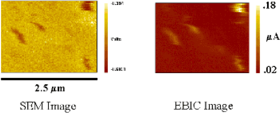
To investigate this hypothesis we have performed electron beam induced current (EBIC) studies. For these measurements diodes with 290 μm diameter ring contact was used which allows the electron beam to directly probe the p-GaN surface. The SEM and EBIC images of such a device are shown in Figure 4. We notice that there is a correspondence between the pits in the p-GaN layer shown in the SEM image and the amount of current conducting through those areas in the EBIC image. Thus, we believe that this result unambiguously correlates the leakage current under reverse bias with the number of dislocations in the material.

Figure 4. SEM (left) and EBIC (right) image of a p-n junction diode. The diode shows larger recombination current at defects revealed in the SEM image.
Conclusions
High quality GaN Schottky diodes have been fabricated on both c-plane sapphire as well as HVPE GaN on sapphire substrates. The homoepitaxially grown diodes are both more conductive under forward bias (37 Ω), as well as less leaky under reverse bias (2.75×10 −4 A/cm2 at –5V) than the heteroepitaxially grown devices. We attribute this to the reduction of dislocations in the homoepitaxially grown MBE GaN layers. Low leakage p-n junction diodes (5×10 −7 A/cm2 at –5V) have also been fabricated by depositing p-GaN by MBE on HVPE GaN on sapphire substrates. EBIC measurements in such devices correlate the leakage current to threading defects. These devices have poor forward bias characteristics which we attribute to poor p-type contacts.
Acknowledgements
The authors are grateful to Dr. Phillip. A. Lamarre and Mr. Dave Parker, Lockheed-Martin Infrared Imaging Sytems, for their assistance with photolithography and C-V measurements. We also thank Dr. Shawn Burke, Dr. Peter McDonald and the Photonics Systems Laboratory for use of their equipment as well as Mr. Paul Mak for his assistance in device fabrication. The authors are grateful to Ms. Worthen and Clariant Corporation for assistance with their photoresist products.The device processing for this work was done in the Optoelectronics Processing Facility at the Boston University Photonics Center. This work was supported by ONR under grant # N00014-99-1-0309, monitored by Dr. Y.S. Park.