


Introduction
Light is composed of three-dimensional (3D) electromagnetic waves that satisfy the Helmholtz equation derived from the Maxwell equations. The propagation of light can be described by optical properties such as amplitude, phase, and wavelength. By controlling the phase of light, the optical wavefront can be tuned. Optical wavefront engineering techniques are indispensable in modern technology, for instance, in microscopy, photolithography, and laser processing. However, conventional techniques to control the phase of light have fundamental limitations.
There are two types of optical lenses, one is typical convex or concave lenses, and the other is echelette lenses, which are compact lenses made by dividing a lens into several concentric annular rings. Convex lenses have been developed for a long time, and their design and manufacturing processes are well optimized. However, shaping 3D spherical surfaces still requires a series of time-consuming processes. Aspherical lenses require more sophisticated processes. They are also bulky and heavy. For instance, typical lenses of digital single-lens reflex cameras weigh approximately 500 g. High-end lenses consisting of more than 20 unit lenses are more than 30 cm long and weigh up to 4 kg.1 In contrast, echelette lenses, which are also called Fresnel lenses, are thin and compact. They can be manufactured by printing methods at low cost, and high focusing efficiency can be achieved in the case of low numerical aperture. However, their focusing efficiency and controllability are drastically degraded as the numerical aperture increases.Reference Lalanne and Chavel2 The drastic height variation at their surfaces disturbs the propagation of transmitted light, therefore, echelette lenses are not enough to replace conventional refractive optical elements.
Metasurfaces that consist of subwavelength optical nanoantennas have provided unprecedented opportunities to overcome the limitations of conventional lenses, and have demonstrated many promising applications such as high-numerical aperture ultrathin lenses,Reference Khorasaninejad, Chen, Devlin, Oh, Zhu and Capasso3 high-resolution multicolor holograms,Reference Yoon, Kim, Mun, Lee, Nam and Rho4 and optical skin cloaks.Reference Ni, Wong, Mrejen, Wang and Zhang5 Various optical properties such as amplitude, phase, and even frequency can be tuned by adjusting the physical shape of individual antennas and their arrangement. Metasurfaces have been developed in terms of structuring materials and design methods to improve their functionality. Plasmonic metasurfaces composed of metallic components suffered from low efficiency in the visible range, but dielectric building blocks can drastically increase the efficiency. Many active materials in which optical properties can be controlled by external voltage bias or temperature modulation have been exploited to dynamically change the optical response of metasurfaces. Computer-assisted design algorithms now enable the design of sophisticated antennas, which can optimize the functionality of metasurfaces.
The articles in this issue of MRS Bulletin review recent progress in metasurfaces, including:
• Novel materials platforms for actively tunable metasurfaces.
• Machine learning algorithms to optimize the functionality of metasurfaces.
• Freeform metasurfaces based on topology optimization.
• Imaging applications of metasurfaces as flat lenses.
Each article discusses discoveries, advantages, and challenges for versatile applications of metasurfaces, providing penetrating insights into the metasurface research area for optical applications.
Materials platforms for metasurfaces
Optical metasurfaces have revolutionized flat-optical technology, and progress has been accelerated by the discovery of new materials. Initial research focused on developing metasurfaces constructed of noble metals such as gold and silver; these metals have high reflectance and plasmonic resonance in visible light. As a result, they can be used in ultrathin (tens of nanometers) devices, and consequently, their nanofabrication is simplified. Versatile deep-subwavelength flat optical applications have been proposed, such as color printing with 100,000 dpi resolution (Figure 1a),Reference Kumar, Duan, Hegde, Koh, Wei and Yang6 or reflective holograms with 80% diffraction efficiency (Figure 1b).Reference Zheng, Mühlenbernd, Kenney, Li, Zentgraf and Zhang7 However, at short-visible wavelengths, noble metals have a high ohmic loss that generates heat; this complicates their implementation as planar optical devices that operate in the entire visible range.

Figure 1. Functional metasurfaces. (a) Full-color image printing based on metal–insulator–metal (MIM) structures. (Left) Optical micrographs of Lena image, (top right) magnified image, and (bottom right) corresponding scanning electron microscope (SEM) image. Scale bar = (left) 1 µm and (right) 500 nm. Reprinted with permission from Reference 6. © 2012 Nature Publishing Group. (b) MIM (gold–magnesium fluoride–gold) structure based on a highly efficient meta-hologram. Adapted with permission from Reference 7. © 2015 Nature Publishing Group. (c) Silicon-based dielectric color printing achieving standard red-green-blue using Kerker’s condition. Optical microscope image of the fabricated dielectric metasurfaces. Scale bar = 20 µm. Reprinted with permission from Reference 13. © 2017 American Chemical Society. (d) TiN-based perfect absorber operating at a high temperature (∼800°C). (Left) SEM image of the fabricated structures and (right) measured absorption spectrum. Reprinted with permission from Reference 16. © 2014 Wiley. (e) High-n (n = index of refraction) nanoresonator based on a transition-metal dichalcogenide. (Left) SEM image of fabricated multilayer WS2 nanodisk array. (Right) The plot explains the in-plane (εxx,yy) and out-of-plane (εzz) dielectric functions of bulk WS2 layer. Inset figure shows a schematic of a multilayer nanodisk and the incidence plane-wave illumination. Reprinted with permission from Reference 20. © 2019 Nature Publishing Group. (f) (Left) Electrically tunable absorber obtained using nanostructured vanadium dioxide. The vanadium dioxide nanostructures are located in the gold bowtie gap structures. (Right) The plot shows tunable absorption based on different heating temperatures. Reprinted with permission from Reference 26. © 2017 American Chemical Society. (g) Switchable color filter based on antimony trisulfide. Reprinted with permission from Reference 28. © 2019 Wiley. The left image shows a color filter with as-deposited antimony trisulfide. The right image shows a color filter with crystalline antimony trisulfide on a hot plate. Using laser irradiation, the area of interest can be amorphized. Note: QWP, quarter-wave plate; k, k0: wave vector; H, magnetic field; E, E0, electric field.
Dielectric-based metasurfaces with Mie resonances, which describe the scattering of matter by the Mie solution to Maxwell’s equations, provide an alternative.Reference Kuznetsov, Miroshnichenko, Brongersma, Kivshar and Luk’yanchuk8 Representative examples of dielectric materials include materials in which the refractive index, n, has a high real part (related to the phase and amplitude of light modulation), but a near zero imaginary part (related to loss) for highly efficient metasurface device. Dielectric-based metasurfaces greatly improve the optical properties of flat optical elements.Reference Khorasaninejad, Chen, Devlin, Oh, Zhu and Capasso3 Specifically, a lens made of such a dielectric,Reference Chen, Zhu, Sanjeev, Khorasaninejad, Shi, Lee and Capasso9,Reference Wang, Wu, Su, Lai, Chen, Kuo, Chen, Chen, Huang and Wang10 and hologram devices have shown high diffraction efficiency in the entire visible wavelength range.Reference Devlin, Khorasaninejad, Chen, Oh and Capasso11,Reference Li, Kim, Zhang, Mehmood, Anwar, Saleem, Lee, Nam, Zhang and Luk’yanchuk12 Also, a dielectric color printing technique that exploits Kerker’s condition, which explains the relationship between balanced electric and magnetic dipoles, showed vivid colors that attained the standard red-green-blue (sRGB) level (Figure 1c).Reference Dong, Ho, Yu, Fu, Paniagua-Dominguez, Wang, Kuznetsov and Yang13
Recently, new materials platforms have been developed that can compensate for the disadvantages of existing plasmonic or dielectric materials (see the Shah et al. article in this issueReference Shah, Kudyshev, Saha, Shalaev and Boltasseva14). For example, conventional plasmonic materials such as copper, silver, and aluminum have poor chemical stability and weak heat resistance. Room-temperature oxidation, sulfidation, and high-temperature degradation have hindered numerous plasmonic applications.Reference Guler, Kildishev, Boltasseva and Shalaev15 As alternatives, the transition-metal nitrides have been proposed as refractory plasmonic platforms with high-temperature durability and good chemical stability. Many intriguing plasmonic applications based on transition-metal nitrides have been introduced, including a TiN-based perfect light absorber that works at high temperature (Figure 1d),Reference Li, Guler, Kinsey, Naik, Boltasseva, Guan, Shalaev and Kildishev16 water splitting,Reference Naldoni, Guler, Wang, Marelli, Malara, Meng, Besteiro, Govorov, Kildishev and Boltasseva17 and photonic spin Hall effect.Reference Chaudhuri, Shaltout, Shah, Guler, Dutta, Shalaev and Boltasseva18 In addition, in optical devices based on dielectric metasurfaces, the refractive index n of the dielectric is not large, so a nanostructure with high aspect ratio (AR) is often required. For example, titanium dioxide (TiO2) or gallium nitride (GaN) require a high AR of 10 to 15, and amorphous silicon requires an AR of 4.7;Reference Ansari, Kim, Lee, Waseem, Zubair, Mahmood, Badloe, Yerci, Tauqeer and Mehmood19 such high values complicate nanofabrication and thus limit further device miniaturization. A Mie resonator has been implemented by stacking atomically thin transition-metal dichalcogenide (TMDC) materials. WS2, a TMDC material, has anisotropic properties with in-plane n ≥ 4, which is much higher than its out-of-plane n (Figure 1e).Reference Verre, Baranov, Munkhbat, Cuadra, Käll and Shegai20
Realization of metadevices has been attempted, and one of the most important goals is the development of technology to actively control metasurfaces.Reference Shaltout, Shalaev and Brongersma21 One approach is to exploit the electrical gating method by modulating the free-carrier density; examples include metasurfaces based on transparent conducting oxides (e.g., indium tin oxide)Reference Huang, Lee, Sokhoyan, Pala, Thyagarajan, Han, Tsai and Atwater22 or highly doped semiconductors (e.g., gallium arsenide).Reference Shcherbakov, Liu, Zubyuk, Vaskin, Vabishchevich, Keeler, Pertsch, Dolgova, Staude and Brener23 However, these materials have the disadvantage of operating mainly in the infrared region because the range of n in the visible region is not large enough to use. Another approach is to use phase-change materials. By tuning the crystallinity or structure of materials, the electrical permittivity can be modulated. For instance, germanium-antimony-tellurium, vanadium dioxide, or antimony trisulfide have been used in active metasurface applications that change the real part of n to near 1. Actual tunable absorber/color (Figure 1f) and filter/hologram devices (Figure 1g) have been developed using these materials.Reference Wang, Rogers, Gholipour, Wang, Yuan, Teng and Zheludev24–Reference Dong, Liu, Behera, Lu, Ng, Sreekanth, Zhou, Yang and Simpson28
Advanced design algorithms for metasurfaces
Inverse design for metasurfaces includes approaches to finding optical components in metasurfaces for given desired functional characteristics.Reference Molesky, Lin, Piggott, Jin, Vucković and Rodriguez29 Despite recent advances in metasurfaces, practical applications have been hampered by complex inverse design problems. Early inverse design methods relied mainly on physical intuition or empirical studies, whereby basic devices were designed by exploiting physical knowledge and suitable optimization processes. However, those approaches encountered significant challenges, because they need to solve complex light–matter interactions.Reference Kruk and Kivshar30,Reference Lin, Liang, Lončar, Johnson and Rodriguez31 Consequently, advanced design algorithmsReference Liu, Gabrielli, Lipson and Johnson32–Reference Jin, Mei, Chen, Li, Zhang, He, Yu, Yu, Yang, Luk’yanchuk, Xiao and Qiu34 for metasurfaces have been developed.
Computational inverse design methods use computational optimization techniques to solve inverse design problems. Computational inverse design methods have been mainly developed by using stochastic-basedReference Huntington, Lauhon and Odom35–Reference Egorov, Eitan and Scheuer37 or gradient-basedReference Hughes, Minkov, Williamson and Fan38–Reference Lalau-Keraly, Bhargava, Miller and Yablonovitch41 optimization algorithms. A genetic algorithm (GA) is one such stochastic-based optimization algorithm, where optimized solutions are searched stochastically based on the concept of natural selection of biological evolution. GAs have been used to determine the structural parameters of metasurfaces,Reference Jafar-Zanjani, Inampudi and Mosallaei33,Reference Huntington, Lauhon and Odom35–Reference Egorov, Eitan and Scheuer37 to design metasurfaces for optical absorbers (Figure 2a)Reference Jafar-Zanjani, Inampudi and Mosallaei33,Reference Bossard, Lin, Yun, Liu, Werner and Mayer36 and for flat beam deflectors.Reference Egorov, Eitan and Scheuer37 However, the computational cost using GAs can be extremely expensive in high-dimensional design spaces, where gradient-following optimization methods are more suitable than GAs.

Figure 2. Advanced algorithms to inversely design metasurfaces. (a) A metasurface for a perfect absorber is designed by a genetic optimization method. (Left) A schematic and (right) the fabricated metasurface systems are shown. In the fabricated images, (top left) a top view and (bottom left) the fabricated of the unit cell structures with scale bar of 200 nm are compared, and (right) low magnification image with scale bar of 600 nm is also presented. Reprinted with permission from Reference 36. © 2014 American Chemical Society. (b) Nonlinear photonic devices are designed by the adjoint method with two exemplary topologies for (left) low and (right) high power pulses routed in different directions. Adapted with permission from Reference 38. © 2018 American Chemical Society. (c) A neural network algorithm for designing H-shaped gold nanostructures is presented. The network takes (top) input information of transmission spectra and provides structural parameters of H-shaped gold nanostructures. Reprinted with permission from Reference 46. © 2018 Nature Publishing Group. (d) A freeform metasurface with arbitrary shape is designed by structural images. The model is composed of two networks, where a generator is used to generate structural images and a discriminator network distinguishes the generated images. Adapted with permission from Reference 56. © 2019 American Chemical Society. Note: DNN, deep neural network; GAN, generative adversarial network; FC, fully connected; conv, convolution; dconv, deconvolution.
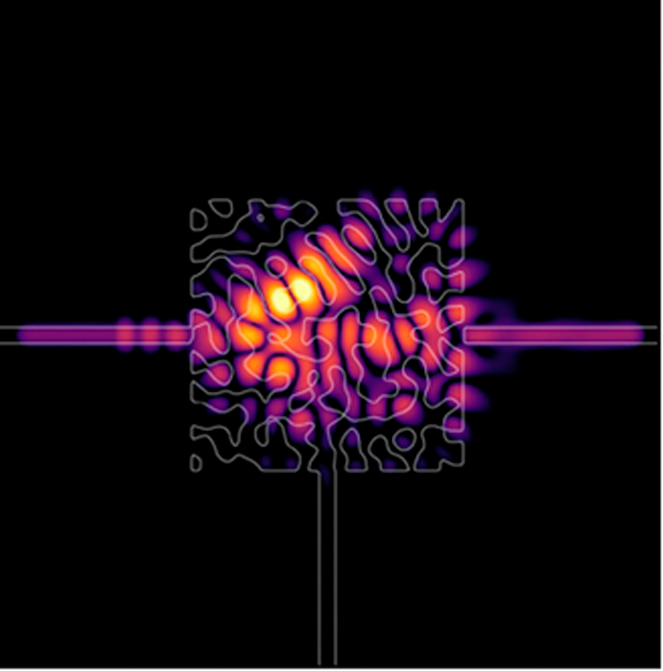
Gradient-based optimization methods incorporate specified objective functions and find optimal solutions mathematically. Topology optimizationReference Lin, Liang, Lončar, Johnson and Rodriguez31 is a mathematics-driven method that optimizes materials over a given design space. It takes advantage of large design freedom, because it performs optimizations over arbitrary domains. As discussed in the Fan article in this issue of MRS Bulletin,Reference Fan42 the gradient-based topology optimization method uses the adjoint variables method (Figure 2b),Reference Hughes, Minkov, Williamson and Fan38 which is based on the Lorentz reciprocity theorem that describes the interchangeability between sources and the electromagnetic fields. It can reduce a heavy computational load, where adjoint equations of linear differential equations are computed instead of a linear combination of eigenvectors, as done in other traditional methods. The adjoint method has enabled incorporation of realistic constraints and computations in arbitrarily large design domains.Reference Phan, Sell, Wang, Doshay, Edee, Yang and Fan43 Metasurfaces for efficient diffractionReference Molesky, Lin, Piggott, Jin, Vucković and Rodriguez29 and a polarizerReference Kruk and Kivshar30 have been designed using the adjoint method. However, setting up the adjoint method for inverse design is a difficult task, so this method has been mainly applied to linear photonic systems. Recent studies have reported nonlinear adjoint methods that solve nonlinear nanophotonic problems.Reference Hughes, Minkov, Williamson and Fan38 The adjoint variable method basically finds a local optimal solution based on gradient descent, where the optimized solution relies on the initial conditions used. Recent studies based on generative neural networks have reported global topology optimizations,Reference Jiang and Fan44,Reference Jiang and Fan45 where a generative neural network is used to generate metasurface candidates for better performance.
Recently, machine learning (ML) has emerged as an alternative to solve complex inverse design problems of metasurfaces,Reference Malkiel, Mrejen, Nagler, Arieli, Wolf and Suchowski46–Reference So and Rho51 as discussed in the Malkiel et al. article in this issue.Reference Malkiel, Mrejen, Wolf and Suchowski52 In ML, which is a subset of the field of artificial intelligence, the system learns a mathematical complex model by consulting past experience or example data.Reference Goodfellow, Bengio and Courville53 In the field of nanophotonics, ML is being used to learn the complex mapping between structural devices and their optical functionalities. In this way, ML has been used to inversely design optical structuresReference Malkiel, Mrejen, Nagler, Arieli, Wolf and Suchowski46–Reference So, Mun and Rho49 and to predict optical functionalitiesReference Sajedian, Kim and Rho54,Reference Qu, Jing, Shen, Qiu and Soljačić55 without the need to conduct computationally intensive numerical simulations. This data-driven approach allows a cost-effective inverse design method, where ML provides appropriate optical structure designs of metasurfaces as outputs for given inputs of desired functionalities. For example, ML using deep neural networks has provided structural parameters of gold nanostructures for a metasurface antenna (Figure 2c),Reference Malkiel, Mrejen, Nagler, Arieli, Wolf and Suchowski46 and a U-shaped antenna for chiral metamaterials.Reference Ma, Cheng and Liu47
An inverse design approach that uses ML has the significant advantage of being capable of handling multiple designs; once the network is trained, it can solve many on-demand design problems within a few seconds for each task. This ability can significantly reduce computational costs. However, such methods of using ML to design structural parameters for given optical functionalities limit the design degrees of freedom. An alternative approach involving designing structural images instead of structural parameters has extended the degree of freedom significantly (Figure 2d).Reference Liu, Zhu, Rodrigues, Lee and Cai50–Reference So and Rho51,Reference Jiang, Sell, Hoyer, Hickey, Yang and Fan56 Structural cross-sectional images are prepared as output forms; as a consequence, arbitrary shapes can be designed. The arbitrary shapes of such designed structures provide for the possibility that inverse design using ML could extend well beyond human intuition.
Metasurfaces for flat lens applications
Since the development of nanoantenna design principles for full-phase manipulation,Reference Yu, Genevet, Kats, Aieta, Tetienne, Capasso and Gaburro57 metalenses have emerged as a promising application of metasurfaces to realize ultrathin light focusing devices without a shadowing effect, which is a fundamental limitation of conventional echelette lenses;Reference Lalanne and Chavel2 see the Lee et al. article in this issue.Reference Lee, Sung and Lee58 Early plasmonic metalenses focused light without spherical aberration, but the focusing efficiency was far too low in the visible range for practical uses.Reference Aieta, Genevet, Kats, Yu, Blanchard, Gaburro and Capasso59,Reference Ni, Ishii, Kildishev and Shalaev60 Basic dielectric components have been investigated to control propagation delays for full-phase manipulation, and it has been verified that dielectric metalenses can achieve extremely high focusing efficiencies, resulting in an enormous number of follow-up studies on metalenses (Figure 3a).Reference Khorasaninejad, Chen, Devlin, Oh, Zhu and Capasso3,Reference Lin, Fan, Hasman and Brongersma61–Reference Khorasaninejad, Zhu, Roques-Carmes, Chen, Oh, Mishra, Devlin and Capasso64 Usually, a dielectric material with high n is required for strong transverse electromagnetic field confinement, which leads to highly efficient full-phase excursion from 0 to 2π.Reference Lalanne and Chavel2

Figure 3. The world seen through metalenses. (a) Monochromatic images of a 1951 US Air Force resolution test chart captured by a high numerical aperture metalens. Magnification varies by operating wavelengths due to chromatic aberration. Scale bars = 500 nm. Reprinted with permission from Reference 3. © 2016 AAAS. (b) A color image captured by an achromatic metalens. Reprinted with permission from Reference 10. © 2018 Nature Publishing Group. (c) In vivo optical coherence tomography imaging of the upper airways of sheep using a metalens catheter. The right image is the magnified dashed blue box on the left image. Note: epi, epithelium; bm, basement membrane; car, cartilage; ves, blood vessel; alv, alveoli. Scale bars = 500 μm. Reprinted with permission from Reference 81. © 2018 Nature Publishing Group. (d, e) Full-color augmented reality (AR) and virtual reality (VR) images, respectively, observed by a see-through metalens. Reprinted with permission from Reference 82. © 2018 Nature Publishing Group.
Flat lenses composed of subwavelength dielectric structures were first demonstrated almost two decades agoReference Lalanne, Astilean, Chavel, Cambril and Launois65–Reference Fattal, Li, Peng, Fiorentino and Beausoleil67 before the rapid increase in metasurface research; nevertheless, dielectric metalenses have recently attracted tremendous attention due to novel functionalities such as achromatic focusing, wide-field imaging, and ultrahigh numerical aperture (NA), which were not realized before. The development of dielectric metalenses has revived the field of flat lenses.
Aberration correction is a chief requirement for a metalens in order to be considered an advanced flat lens. A quadratic phase gradient, which is required for a perfect lens, perfectly removes the spherical aberration;Reference Aieta, Genevet, Kats, Yu, Blanchard, Gaburro and Capasso59 therefore, efforts have shifted to compensating for chromatic aberration, which is a fundamental phenomenon of diffractive optical elements. Dispersive phase compensation that utilizes the dispersion of nanostructures has been widely investigated for this (Figure 3b),Reference Chen, Zhu, Sanjeev, Khorasaninejad, Shi, Lee and Capasso9,Reference Wang, Wu, Su, Lai, Chen, Kuo, Chen, Chen, Huang and Wang10,Reference Aieta, Kats, Genevet and Capasso68–Reference Chen, Zhu, Sisler, Bharwani and Capasso72 and innovative design principles have been established to eliminate chromatic aberration by using a single metalens.
Other methods can be used to realize achromatic metalenses. Spatial multiplexing of metalenses that operate only for each target wavelength is a straightforward method to induce different phase gradients by wavelengths.Reference Arbabi, Arbabi, Kamali, Horie and Faraon73–Reference Lin, Holsteen, Maguid, Wetzstein, Kik, Hasman and Brongersma75 Chromatic aberration can also be compensated by superposing several metalenses along the optical axis.Reference Zhou, Kravchenko, Wang, Nolen, Gu and Valentine76 Another significant breakthrough in metalens research is the ability to compensate for coma aberration in off-axis illumination; this aberration, which causes off-axis incident light rays to appear as comet-like tails, disturbs wide-field imaging. Coma aberration can be corrected by a doublet composed of a phase-compensating metasurface stacked on a metalens.Reference Arbabi, Arbabi, Kamali, Horie, Han and Faraon77,Reference Groever, Chen and Capasso78 State-of-the-art metalens doublets yield a consistent focal spot up to an incident angle of 30°; this is a remarkable improvement over single metalenses, in which focal spots deteriorate even at 1° off-axis illumination. High NA is another advantage of metalenses. Typical metalenses can easily achieve high NAs of 0.8, but it can be further increased up to 0.99 by exploiting diffracted energy redistribution in asymmetrically shaped nanoantennas.Reference Paniagua-Domínguez, Yu, Khaidarov, Choi, Leong, Bakker, Liang, Fu, Valuckas, Krivitsky and Kuznetsov79
Metalenses have demonstrated many promising applications for next-generation flat optical devices. Miniaturized imaging modules that consist of metalenses combined with image sensors are representative examples that allow development of compact planar cameras, and their functionalities can be further improved by using microelectromechanical systems of tunable metalenses in which the focal length can be controlled in real time by adjusting an external voltage bias.Reference She, Zhang, Shian, Clarke and Capasso80 Metalenses can be applied to endoscopic catheters to overcome conventional graded-n or ball-shaped lenses, which suffer from aberrations due to asymmetric curvatures of the protective outer sheath of the endoscopic catheter.Reference Pahlevaninezhad, Khorasaninejad, Huang, Shi, Hariri, Adams, Ding, Zhu, Qiu, Capasso and Suter81 Metalenses can be designed to perfectly compensate for such undesired phase distortion; the resolution of in vivo optical coherence tomography can be much higher than that of conventional optical tomography (Figure 3c). Augmented reality (AR) and virtual reality (VR) devices are emerging as realistic display techniques to provide immersive perception, but current AR and VR devices suffer from a narrow field of view and large form factor. These limitations can be overcome by using see-through metalenses that have the dual functionality of focusing and bypassing for opposite incident polarization states (Figure 3d–e).Reference Lee, Hong, Hwang, Moon, Kang, Jeon, Kim, Jeong and Lee82 Because the see-through metalenses can be placed closer to user eyes, the field of view can be improved and the form factor can be reduced, as compared to conventional lenses.
Metasurfaces for display applications
Substantial efforts have been directed toward the use of optical metasurfaces as displays (e.g., for color generation and holography).Reference Kumar, Duan, Hegde, Koh, Wei and Yang6,Reference Zheng, Mühlenbernd, Kenney, Li, Zentgraf and Zhang7 Colors generated by a metasurface are determined by the geometry of nanostructures on the surface, similar to structural colors in nature. An array of nanostructures on a metasurface resonates at a certain frequency in the visible spectrum; this phenomenon can be exploited to modulate the power of transmitted and reflected light in the visible regime. In holograms that use metasurfaces, the meta-atoms in each pixel are designed to match the complex amplitude of incident light with those required for image reconstruction.Reference Ni, Kildishev and Shalaev83
Initially, metals were considered for use as a constitutive material of a metasurface for coloration due to advancements in plasmonics.Reference Goh, Zheng, Tan, Zhang, Kumar, Qiu and Yang84–Reference Rezaei, Hong Ng, Dong, Ho, Koay, Ramakrishna and Yang86 Subwavelength-sized meta-atoms enabled the realization of ultrahigh display resolution below the diffraction limit of light. However, the inevitable lossy nature of a metal hinders generation of vivid colors, so lossless materials have been sought. High-n dielectric resonators such as silicon and TiO2 have been explored as new candidates.Reference Dong, Ho, Yu, Fu, Paniagua-Dominguez, Wang, Kuznetsov and Yang13,Reference Jang, Jeong, Hu, Qiu, Nam and Rho87,Reference Yang, Liu, Li, Cheng, Choi, Chen and Tian88 A recent advance in the understanding of directional scattering in a high-n dielectric Mie-resonatorReference Paniagua-Domínguez, Yu, Miroshnichenko, Krivitsky, Fu, Valuckas, Gonzaga, Toh, Kay, Luk’yanchuk and Kuznetsov89 has enabled design of a dielectric nanostructure to increase reflection or transmission and to suppress unwanted scattering, yielding a color gamut that exceeds standard red green blue (sRGB).Reference Dong, Ho, Yu, Fu, Paniagua-Dominguez, Wang, Kuznetsov and Yang13,Reference Jang, Jeong, Hu, Qiu, Nam and Rho87,Reference Yang, Liu, Li, Cheng, Choi, Chen and Tian88 However, coloration by a metasurface is static—once the device is fabricated, its colors cannot be tuned. Accordingly, research has been conducted to achieve tunable or dynamic color of metasurfaces by exploiting the polarization-dependent response of asymmetric nanostructures,Reference Jang, Jeong, Hu, Qiu, Nam and Rho87,Reference Franklin, Frank, Wu and Chanda90 liquid crystals,Reference Franklin, Frank, Wu and Chanda90,Reference Olson, Manjavacas, Basu, Huang, Schlather, Zheng, Halas, Nordlander and Link91 and metal-to-dielectric transition.Reference Duan and Liu92–Reference Chen, Duan, Matuschek, Zhou, Neubrech, Duan and Liu94 Such efforts have shown that metasurfaces have the potential for use in next-generation displays.
Holography can replicate the recorded complex amplitude distribution of an object so that, in theory, the observer cannot differentiate the outgoing wave of the hologram from the real one. This feature has possible applications in 3D displays for virtual and augmented reality.Reference Franklin, Frank, Wu and Chanda90 Ultrathin plasmonic metasurfaces (subwavelength-scale thickness) that exploit phase modulation by the metasurface have been proposed.Reference Ni, Kildishev and Shalaev83 The complementary nanoantennas with two arms allows amplitude modulation and phase shifting by changing the arm length and the splitting angle. However, the 2π phase excursion was rather complicated because designing two-armed nanoantennas with a phase delay is not straightforward. A simple design method that exploits the Pancharatnam–Berry phase, which simply encodes the phase delay twice that of the given rotation angle of nanorods, under illumination by circularly polarized light enables to achieve optical holography by plasmonic nanorods to replace a holography plate.Reference Zheng, Mühlenbernd, Kenney, Li, Zentgraf and Zhang7 A metal-dielectric-metal configuration in reflection mode achieved a hologram that had 80% diffraction efficiency at a wavelength of 825 nm. Compared to metallic components, a hologram produced by an all-dielectric metasurface shows superior efficiency, particularly in transmission. Hence, various highly efficient metasurfaces composed of Si, TiO2, or GaN have been suggested.Reference Devlin, Khorasaninejad, Chen, Oh and Capasso11,Reference Kim, Yoon, Jang, Genevet, Nam and Rho95
Research toward optical metasurfaces has been broadened to include multiplexingReference Kamali, Arbabi, Arbabi, Horie, Faraji-Dana and Faraon96–Reference Wang, Dong, Li, Yang, Sun, Chen, Song, Xu, Chu, Xiao, Gong and Li101 and multifunctional devices.Reference Yoon, Lee, Nam and Rho102–Reference Liu, Xu, Wang, Liu, Ruan, Wu, Liu and Yang105 Multiplexed metasurface holograms can reconstruct two distinct images under illumination by left and right circularly polarized light.Reference Wen, Yue, Li, Zheng, Chan, Chen, Chen, Li, Wong, Cheah, Pun, Zhang and Chen97 Multichannel holography can render different sets of images with a total of 12 polarization channels.Reference Zhao, Sain, Wei, Tang, Li, Weiss, Huang, Wang and Zentgraf99 Multicolor holography can reconstruct three different images under red, green, and blue laser illumination in a single device.Reference Li, Chen, Li, Zhang, Pu, Zhao, Ma, Wang, Hong and Luo100,Reference Wang, Dong, Li, Yang, Sun, Chen, Song, Xu, Chu, Xiao, Gong and Li101 A single metasurface that works simultaneously under coherent and incoherent light has been suggested;Reference Yoon, Lee, Nam and Rho102–Reference Kim, Yoon, Baek, Rho and Lee104 this device generates structural colors under ambient light and reconstructs a hologram under a coherent laser source. By exploiting metasurface coloration, two independent images can be encoded, one hidden and one visible. The surface uses pixels that have embedded upconversion nanoparticles (NPs), so the hidden image is only revealed under illumination by a laser at 980-nm wavelength, because the NPs fluoresce only under such conditions. These features have obvious applications in optical steganography and cryptography, where they involve techniques that conceal/hide a message or information for security purposes.Reference Jang, Jeong, Hu, Qiu, Nam and Rho87,Reference Yoon, Lee, Nam and Rho102,Reference Lim, Liu, Liu and Yang103,Reference Liu, Xu, Wang, Liu, Ruan, Wu, Liu and Yang105
Nonlinear and quantum metasurfaces
Using metasurfaces with subwavelength control over polarization enables control of nonlinear optical processes, such as second-harmonic and third-harmonic generationReference Li, Chen, Pholchai, Reineke, Wong, Pun, Cheah, Zentgraf and Zhang106 (as discussed in the Pertsch and Kivshar article in this issueReference Pertsch and Kivshar107) and four-wave mixing.Reference Li, Sartorello, Chen, Nicholls, Li, Zentgraf, Zhang and Zayats108 Symmetry selection rules in harmonic generation have been observed in nonlinear optical chirality using meta-atoms, or the artificial atoms constituting the metasurfaces.Reference Chen, Li, Zeuner, Wong, Pun, Zentgraf, Cheah and Zhang109,Reference Chen, Zeuner, Weismann, Reineke, Li, Valev, Cheah, Panoiu, Zentgraf and Zhang110 Nonlinear geometric Berry phase and nonlinear spin–orbit interactions have been observed using metasurfaces,Reference Li, Sartorello, Chen, Nicholls, Li, Zentgraf, Zhang and Zayats108,Reference Chen, Zeuner, Weismann, Reineke, Li, Valev, Cheah, Panoiu, Zentgraf and Zhang110–Reference Li, Wu, Li, Chen, Schlickriede, Xu, Huang, Li, Liu, Pun, Zentgraf, Cheah, Luo and Zhang112 and nonlinear wavefront engineeringReference Almeida, Shalem and Prior113,Reference Li, Zhang and Zentgraf114 can be achieved using metasurfaces.
Temporal and spectral responses are related by the Fourier transformation, so temporal or spectral (frequency) modulation of one response leads to the modulation of the other. Linear frequency conversion using time-variant metasurfaces has been demonstrated.Reference Lee, Son, Park, Kang, Jeon, Rotermund and Min115 Spatiotemporal beam scanning using metasurfaces was achieved using laterally resolved spectrally modulated metasurfaces, which control the wavefront using a frequency gradient as opposed to using a conventional phase gradient.Reference Shaltout, Shalaev and Brongersma21,Reference Shaltout, Lagoudakis, van de Groep, Kim, Vučković, Shalaev and Brongersma116
Integrated with quantum emitters, metasurfaces could be used as a platform for quantum photon sources. In a weak coupling regime, Purcell enhancement of quantum emitters, or their enhancement of spontaneous emission rates, could enable the development of efficient single-photon sources for quantum optics. High efficiency in these devices requires a collection of photons and control over their emission directivity. Atomically thin two-dimensional materials such as graphene, hexagonal boron nitride, and TMDCs can also serve as quantum photon sources. Compared to quantum dots, these materials can be more easily integrated into photonic circuitry.
Due to long quantum coherence lifetimes, photons are advantageous for constructing quantum information processing units. Metasurfaces have also been suggested for use in quantum optics to control additional degrees-of-freedom in polarization states. Recently, generation of photons with entangled spin and orbital angular momentumsReference Stav, Faerman, Maguid, Oren, Kleiner, Hasman and Segev117 and multiphoton quantum statesReference Wang, Titchener, Kruk, Xu, Chung, Parry, Kravchenko, Chen, Solntsev, Kivshar, Neshev and Sukhorukov118 were achieved using low-loss dielectric metasurfaces, which are advantageous over plasmonic metasurfaces, because losses degrade quantum coherence. Use of metasurfaces has enabled the generation, manipulation, and measurement of quantum states of light integrated on a single on-chip device.
Outlook
Over the past 10 years, metasurfaces have demonstrated their possibility as future optical technologies to overcome the fundamental limitations of conventional optical techniques. The development of optical technology stimulates the development of other fields such as physics, chemistry, and biology, so metasurfaces as novel techniques for light control will significantly contribute to the further development of modern scientific technology. We hope the articles in this issue can inspire researchers to utilize metasurfaces in a broad range of research fields.
Acknowledgments
We express our gratitude to all of the authors for their contributions to this issue of MRS Bulletin. J.R. acknowledges the National Research Foundation Grants (Nos. NRF-2019R1A2C3003129, CAMM-2019M3A6B3030637, NRF-2019R1A5A8080290, and NRF-2018M3D1A1058998) funded by the Ministry of Science and ICT (MSIT), Republic of Korea.

Junsuk Rho is a Mu-Eun-Jae Endowed Chair Associate Professor in the Department of Mechanical Engineering and the Department of Chemical Engineering at Pohang University of Science and Technology (POSTECH), Republic of Korea. He received his PhD degree in mechanical engineering from the University of California, Berkeley, in 2013, his MS degree in mechanical science and engineering from the University of Illinois at Urbana-Champaign, in 2008, and BS degree in mechanical and aerospace engineering from Seoul National University, Republic of Korea, in 2007. Rho completed postdoctoral research in the Materials Sciences Division and Molecular Foundry at Lawrence Berkeley National Laboratory. He was also a principal investigator (Ugo Fano Fellow) in the Nanoscience and Technology Division and the Center for Nanoscale Materials at Argonne National Laboratory. His awards include the MRS Graduate Student Award (2011), the OSK Young Investigator Award (2016), SPIE, (the International Society for Optics and Photonics) Rising Researcher Award (2017), a Korean Ministry of Science and ICT Minister’s Commendation (2019), and the Korean Presidential Early Career Award for Scientists and Engineers (2019). Rho can be reached by email at jsrho@postech.ac.kr.


