Introduction
Lateral transport in lightly doped n-GaN thin films has been extensively studied, most often by using Hall effect measurements. These studies indicate that electron transport in the lateral direction is dominated by scattering from charged dislocations, which serves to reduce the electron mobility.[Reference Ng, Doppalapudi, Moustakas, Weimann and Eastman1-Reference Weimann, Eastman, Doppalapudi, Ng and Moustakas2] Based on this model, transport in the vertical direction should be relatively unaffected by the presence of the threading dislocations and electron mobility should be significantly increased. Since a large number of GaN devices, including lasers, LEDs, detectors and bipolar junction transistors [Reference Nakamura, Pankove and Moustakas3-Reference Moustakas, Pankove and Moustakas5], have vertical geometry, it is important to investigate electron mobility in this direction to better understand and engineer device performance.
In this paper we have used Schottky barrier diodes, fabricated with a vertical geometry on lightly doped n-GaN films grown by ECR-MBE, to investigate electron mobility for vertical transport. The diodes were evaluated by I-V and C-V measurements to determine diode ideality, reverse saturation current, doping concentration and barrier height. Using the diffusion model for current transport in Schottky barriers, mobility for vertical transport was determined. The results are compared with lateral electron mobility determined by Hall Effect measurements.
Experimental Methods
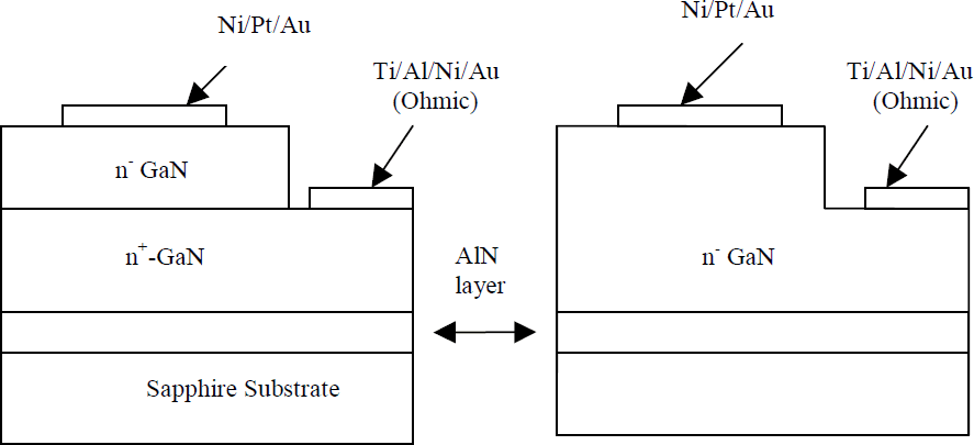
The GaN films were grown on c-plane sapphire, by plasma-assisted molecular beam epitaxy, following procedures described earlier.[Reference Moustakas, Pankove and Moustakas5] In this paper we present only a brief description. Prior to introduction into the growth chamber, the substrates were subjected to solvent degreasing. The Al2O3 surface was converted to AlN by exposing the substrate, held at 800 °C, to nitrogen plasma using an electron cyclotron resonance (ECR) microwave plasma source. This step was followed by the deposition of 1000 Å AlN buffer. Two types of devices (Figure 1) were investigated. In the first, 2.25 µm thick n+ GaN (2×1018 cm−3) was deposited first, followed by a n− GaN (1×1017 cm−3) of about the same thickness.The second device consists of 4 µm thick n- GaN (1×1017 cm−3). All the layers were grown under Ga rich conditions. RHEED patterns, taken during growth of the n-GaN layers, showed 2×2 surface reconstruction, indicating that the films were grown with the Ga-polarity.[Reference Smith, Feenstra, Greve, Shin, Skowronski and Neugebauer6]

Figure 1: Schematic illustration of the two types of devices investigated.
Circular mesas, approximately 3 µm deep and 300 µm in diameter, were defined on both samples by reactive ion etching, using Cl2 gas. Ohmic contacts were defined on the bottom of the mesa by electron beam deposition of 200/1000/200/2500Å Ti/Al/Ni/Au metal multilayers. The Ohmic contacts were rapid thermal annealed at 750°C for 60 seconds, prior to deposition of the Schottky contacts. Schottky contacts were formed at the top of the mesa by patterning 200 µm dots by photolithography and depositing a 200/1000/3000Å Ni/Pt/Au metal multilayer stack by electron beam evaporation. Some of the diodes were mounted on transistor headers and Au wires were bonded to the contacts by thermosonic bonding. Figure 1 shows a schematic illustration of the two types of samples reported in this paper.
Hall Effect measurements were performed on the n-GaN films by the Van der Pauw method, using indium contacts in the clover leaf configuration. Current–voltage characteristics were measured using the HP 4155A semiconductor parameter analyzer. Capacitance-voltage measurements were performed using the HP 4275A LCR measurement system. For some of the type II devices, Ohmic contacts were deposited at the top and bottom of the mesas, and their I-V characteristics were evaluated.
Experimental Results
The current voltage characteristics for the structures with Ohmic contacts at both ends are shown in Figure 2. The resistance of the devices was measured to be in the 3-10 Ω range. In order to investigate the origin of this resistance, I-V measurements were performed as a function of temperature. The resistance was found to slightly increase with temperature, while our evidence from planar Hall effect measurements indicate that the resistance decreases with temperature. This suggests that the measured resistance in the vertical direction using two ohmic contacts is dominated by the contacts rather than the bulk GaN resistance. From the data of Fig. 2, the specific contact resistivity was estimated to be on the order of 10−3 Ω*cm2. Such values of contact resistivity for lightly doped GaN layers are quite typical [Reference Sampath7]. This observation has important implications for vertical devices with high-mobility layers because it indicates that in order to obtain the maximum current carrying capacity of the active layer, the Ohmic contact resistance must be brought down by several orders of magnitude.

Figure 2: I-V characteristics of veritical GaN resistors measured as described in the text at different temperatures.
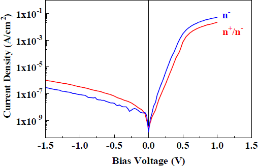
Typical current voltage characteristics of the two types of Schottky barrier diodes investigated are shown in Figure 3.

Figure 3: Typical I-V characteristics of the two types of Schottky barrier diodes
In the forward direction the data can be fitted to Eq. 1. where Jo is the saturation current density and n is the ideality factor. Applying Eq. 1 to the data of Figure 3, we find that the diodes are practically ideal (n=1.15−1.2) and the value of the reverse saturation current densities for the n+/n− and n−-GaN samples are 1.08 × 10⁻⁹ A/cm2 and 1.0 × 10⁻⁸ A/cm2 respectively. A number of devices were probed on each wafer, and found to give very good uniformity over an area approximately equal to a quarter of a 2” wafer.

Results of the capacitance-voltage measurements are shown in Fig. 4. The doping concentration and barrier height were determined from the C-V measurements, using the following equation [Reference Sze8]:

where C is the measured capacitance, V is the applied voltage, Vbi is the built-in voltage, εs is the dielectric constant, Nd is the doping concentration and Ae is the geometric area of the device. The barrier height is given by

where Nc is the effective density of states in the conduction band.

Figure 4: C-V plots for the two types of Schottky barrier diode structures investigated.
The doping concentration and barrier height obtained by fitting the data of Fig. 4 to Eqs. (2) and (3), were determined to be 9×1016 cm−3 and 1.0 V for the n+/n − -GaN diode, 8.4×1016 cm−3 and 0.95 V for the n − -GaN diode. These results are in general agreement with those reported earlier. [Reference Schmitz, Ping, Asif Khan, Chen, Yang and Adesida9-Reference Wang, Nathan, Lim, Khan and Chen10] A number of devices, fabricated on the same wafer were tested and were found to give similar values of barrier heights, doping concentration and reverse saturation current densities.
Discussion
The carrier concentration in the two types of samples was determined by measuring the Hall effect on the n − -GaN films as well as by measuring the capacitance voltage characteristics of both types of Schottky barrier diodes.
From the Hall effect measurements, the carrier concentration of the n − -GaN film was determined to be 1.4 x1017 cm−3 and the lateral mobility (µl) was 160 cm2/V-s. Although the dislocation densities in these particular samples have not been measured, from measurements on samples grown under similar conditions, the threading dislocation density is estimated to be in the range of 5-10×109cm−2. As discussed previously, the lateral electron mobility in our samples attains its highest value at 300-400 cm2/V-s at carrier concentrations of 3-5×1017 cm−3 and then it reduces at lower carrier concentrations. This result was accounted for by scattering from negatively charged dislocations [Reference Ng, Doppalapudi, Moustakas, Weimann and Eastman1,Reference Weimann, Eastman, Doppalapudi, Ng and Moustakas2].
In order to investigate the electron mobility for vertical transport, the diffusion theory of Schottky barriers, which expresses the relation between the reverse saturation current as a function of barrier height and the diffusion coefficient of electrons in the space charge region was employed. According to this model, the reverse saturation current density is given by the relation [Reference Spenke11]

where µv is the electron mobility in the vertical direction. Using the values of J0, Nd, ϕ and Vbi in Eq. (4), we obtain a vertical mobility of µv=932 cm2/V-s for the n+/n − GaN and µv =949 cm2/V-s for the n − -GaN film.
In the calculation of the vertical mobility, we have assumed that the active area is equal to the geometric area of the device. A reduction of the active area (up to one-third for dislocation density of 5×109 cm−2 and doping concentrations of 1×1017cm−3) is expected due to depletion around each charged dislocation. Specifically, considering the active area to be two- thirds the geometric area, increases the doping concentration and reverse saturation current density to be 1.9×1017 cm−3, 1.62×10⁻⁹ A/cm2 respectively for the n+/n− device. This leads to a vertical mobility of 1070 cm2/V-s for the same device. These results are in good agreement with Monte-Carlo calculations for electron mobility in GaN thin films.[Reference Weimann, Eastman, Doppalapudi, Ng and Moustakas2]
Conclusions
Investigation of lateral and vertical transport in n − -GaN films indicates that for samples doped at the level of 1×1017 cm−3, the vertical mobility is more than six times higher than the lateral mobility. This result is attributed to the reduction of electron scattering by charged dislocations during vertical transport.
Acknowledgements
We wish to thank Prof. C.R Eddy and Dr. N.G. Weimann for useful discussions. We are grateful to Dr. P.A. Lamarre and Mr. D. Parker of Lockheed-Martin for help with device fabrication and C-V measurements and Mr. P. Mak of the Photonics Center at Boston University for help with packaging of the devices. The authors are grateful to Ms. Worthen and Clariant Corporation for assistance with their photoresist products. The device processing for this work was done in the Optoelectronics Processing Facility at the Boston University Photonics Center. This work was supported by ONR under grant # N00014-99-1-0453, monitored by Dr. J. C. Zolper.