Introduction
InGaN-based laser diodes have potential in a number of applications such as optical storage, printing, full-color displays, chemical sensors and medical applications. Major developments in recent years have led to lifetimes in excess of 10,000 hours, demonstrating the viability of nitride laser diodes for commercial applications [Reference Nakamura, Senoh, Nagahama, Iwasa, Yamada, Matsushita, Kiyoku, Sugimoto, Kozaki, Umemeto, Sano and Chocho1]. The implementations of lateral epitaxial overgrowth (LEO) and AlGaN/GaN modulation-doped strained-layer superlattices in the laser structure have led to increased lifetimes [Reference Nakamura, Senoh, Nagahama, Iwasa, Yamada, Matsushita, Kiyoku, Sugimoto, Kozaki, Umemeto, Sano and Chocho2]. Strained-layer superlattices are used for strain relief to prevent cracking in the cladding layers [Reference Ito, Hiramatsu, Amano and Akasaki3], and the LEO technique has been shown to reduce the threading dislocation density in GaN grown by metalorganic chemical vapor deposition (MOCVD) [Reference Kapolnek, Keller, Vetury, Underwood, Kozodoy, DenBaars and Mishra4-Reference Marchand, Ibbetson, Fini, Kozodoy, Keller, Speck, DenBaars and Mishra7] and hydride vapor phase epitaxy (HVPE) [Reference Usui, Sunakawa, Sakai and Yamaguchi8,Reference Sakai, Sunakawa and Usui9].
This reduction in dislocation density leads to benefits in device performance such as lower reverse-bias leakage current of p-n junction diodes [Reference Kozodoy, Ibbetson, Marchand, Fini, Keller, Keller, Speck, DenBaars and Mishra10] and LEDs [Reference Sasaoka, Sunakawa, Kimura, Nido, Usui and Sakai11,Reference Nakamura, Senoh, Nagahama, Iwasa, Matushita and Mukai12] low gate leakage current in AlxGa1‒xN FETs [Reference Vetury, Marchand, Ibbetson, Fini, Keller, Speck, DenBaars and Mishra13] and low dark current, sharp cutoff AlxGa1‒xN-based solar-blind photodetectors [Reference Parish, Keller, Kozodoy, Ibbetson, Marchand, Fini, Fleischer, DenBaars, Mishra and Tarsa14]. These results suggest the presence of mid-gap states associated with dislocations. For high quality coalesced LEO GaN, factors such as tilt misalignment between adjacent stripes must be carefully considered. The overgrown GaN wings have been shown to exhibit a tilt away from the seed region perpendicular to the stripe direction for both MOCVD [Reference Ito, Hiramatsu, Amano and Akasaki3,Reference Marchand, Ibbetson, Fini, Chichibu, Rosner, Keller, DenBaars, Speck and Mishra15] and HVPE [Reference Usui, Sunakawa, Sakai and Yamaguchi8,Reference Tsukamoto, Taki, Kuwano, Oki, Shibata, Sawaki and Hiramatsu16] grown LEO GaN oriented in the < 1

Experimental Details
In this study, laser diodes were fabricated on high quality fully-coalesced LEO GaN leading to improved device performance. Lasers fabricated on the LEO wings, along with coalescence fronts containing few or no threading dislocations, exhibit a reduced threshold current density compared to those grown on conventional planar GaN on sapphire. The internal quantum efficiency increased from 3% to 22%.
InGaN multiple-quantum-well (MQW) laser diodes were grown by MOCVD in a two-flow horizontal reactor at both atmospheric and low pressure. In preparation for patterning a subsequent regrowth, a 2 µm thick GaN seed layer was grown on a c-plane sapphire substrate. A 2000 Å SiO2 mask was patterned into stripes, oriented in the <1
Laser diodes were fabricated above the SiO2 mask in the nearly dislocation-free wing regions, above the coalescence fronts of the LEO GaN stripes, as well as above the dislocated window (seed) region. The laser cavity was oriented parallel to the direction of the SiO2 stripes. Laser facets were formed by Cl2 reactive ion etching (RIE) of 45 µm wide mesas of various lengths ranging from 400 µm to 1600 µm and p-contact stripes were patterned on these mesas with widths ranging from 5 µm to 15 µm. The structure was etched around the p-contact stripe through the p-cladding for index guiding. The n and p-contacts were formed by electron beam evaporation of Ti/Al and Pd/Au, respectively. Electrical testing was performed using 50 ns pulses with a 1 kHz pulse repetition rate.
Results
Figure 1 shows cross-section TEM micrographs of the coalescence region. There are few or no threading dislocations (with a linear density <4×103 cm−1) generated at the coalescence fronts. This high quality coalescence results from low wing tilts of the laterally growing stripes. The LEO wings have a tilt of 0.1° relative to the underlying seed material, which was measured using x-ray diffraction as described earlier [Reference Fini, Zhao, Moran, Hansen, Marchand, Ibbetson, DenBaars, Mishra and Speck18].

Figure 1. Bright-field cross-section TEM micrographs of a coalescence front viewed with (a) g = 0002 and (b) g = 11
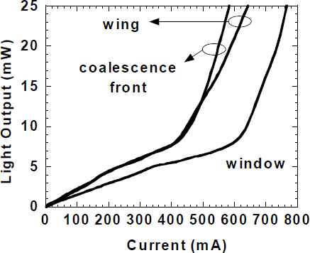
Figure 2 shows the typical light output per uncoated facet of 5×1200 µm2 laser diodes grown on LEO GaN as a function of forward current under pulsed operation, The laser diodes are placed above the wing, window and coalescence front regions. The threshold current for the laser placed on the wing, window and coalescence front regions is 340 mA, 570 mA and 380 mA respectively, resulting in respective threshold current densities of 5.7 kA/cm2, 9.5 kA/cm2, and 6.3 kA/cm2. The corresponding threshold voltages were 15.2 V, 17 V, and 16.1 V for lasers on the wing, window and coalescence fronts respectively. The minimum threshold current density was reduced by a factor of 2 from 8 kA/cm2 for laser diodes placed on the wing region to 3.7 kA/cm2 for laser diodes placed on the window region. Laser diodes grown on LEO GaN were also compared to those grown on sapphire. The minimum threshold current density was reduced by a factor of 2 from 10 kA/cm2 for laser diodes grown on sapphire to 4.8 kA/cm2 for laser diodes grown on LEO GaN on sapphire. The laser diodes on the LEO GaN showed this low threshold current density of 4.8 kA/cm2 both above the SiO2 mask regions and above the coalescence fronts of the LEO GaN. Unlike the threshold current density, the threshold voltage was not reduced as dramatically for the lasers grown on LEO GaN. The minimum threshold voltage was 21.8 V for lasers on LEO GaN compared to 17.4 V for lasers on GaN/sapphire. This reduction in threshold current density is attributed to a reduction in nonradiative recombination due to the lower dislocation density in the LEO GaN.

Figure 2. Typical light output per uncoated facet as a function of current for 5×1200 µm2 laser diodes placed on the wing, window and coalescence front on LEO GaN.
Figure 3 shows the reciprocal of external differential quantum efficiency as a function of length for laser diodes grown on sapphire and LEO GaN. The external differential quantum efficiency of the laser diode increases with increasing internal quantum efficiency or decreasing internal optical loss as seen in the following relationship [Reference Coldren and Corzine19],

where ηd is the external differential quantum efficiency, ηi is the internal quantum efficiency, αm is the mirror loss and αi is the internal optical loss of the laser. The mirror loss can be defined as
where L is the length and R is the facet reflectivity. R is estimated to be approximately 0.053 for RIE etched facets [Reference Mack, Via, Abare, Hansen, Kozodoy, Keller, Speck, Mishra, Coldren and DenBaars20]. Substituting equation 2 into equation 1 and rearranging gives


Figure 3. Inverse external differential quantum efficiency as a function of device length.
The internal quantum efficiency can be extracted from the y-intercept of figure 3 using equation 2. The increase in external differential quantum efficiency seen in the lasers on LEO GaN compared to those on sapphire is due to a increase in the internal quantum efficiency from ∼3% to ∼22%. As mentioned, the reduced reverse bias leakage current in p-n junction diodes suggests the presence of mid-gap states due to threading dislocations [Reference Speck and Rosner21]. These mid-gap states provide nonradiative recombination centers thereby decreasing the internal quantum efficiency. Reducing the dislocation density, and hence the mid-gap states, will result in an increased internal quantum efficiency. The same effect is also seen in the spontaneous emission portion of L-I curve below threshold in figure 2 as well as in LEDs fabricated on LEO GaN [Reference Sasaoka, Sunakawa, Kimura, Nido, Usui and Sakai11,Reference Hansen, Fini, Abare, Coldren, Speck and DenBaars22], where the radiative efficiency increases with decreasing dislocation density.
Conclusions
In summary, InGaN multi-quantum well laser diodes have been fabricated on fully coalesced laterally overgrown GaN on sapphire. The wing regions as well as the coalescence regions of the LEO GaN contain few or no threading dislocations. The threshold current density was reduced by a factor of 2 from 10 kA/cm2 for laser diodes grown on sapphire substrates to 4.8 kA/cm2 for laser diodes grown on LEO GaN on sapphire. Laser diodes fabricated on the wing regions also showed a factor of 2 improvement as compared to those on the window regions from 8 kA/cm2 to 3.7 kA/cm2. The internal quantum efficiency also improved from 3% for laser diodes on conventional GaN on sapphire to 22% for laser diodes on LEO GaN on sapphire. This increase is attributed to a reduction of nonradiative recombination from a reduced dislocation density.
Acknowledgements
The authors will like to acknowledge funding support from DARPA (R. Leheny), NSF, ONR (Max Yoder, Colin Wood, Yoon-Soo Park) and Hewlett-Packard (S.Y. Wang) through the UC MICRO program.