Introduction
The continuing improvement of group III-nitride compound semiconductor material quality has led to the demonstration of viable AlGaN/GaN heterostructure field effect transistors (HFETs) with widths up to 1mmReference Nguyen, Nguyen and Grider 1 , suitable for high power amplifiers. For these applications self-heating of the device is important and, since the heat is conducted out of the active region through the substrate, the thermal properties of the substrates play a significant role in the device performance. The traditional sapphire substrate has shown itself to be inadequate and recent GaN-based power amplifier devicesReference Xu, Wu, Keller, Parish, Heikman, Thibeault, Mishra and York 2 have explored new substrate materials. Alternative substrates include SiC, GaN, and AlN, which offer enhanced thermal conductivities. Power densities as large as 6.9 W/mm at 10GHz have been demonstrated for GaN-based devices on SiCReference Sheppard, Doverspike, Pribble, Allen, Palmour, Kehias and Jenkins 3 . Here, we present a comparison of the DC output characteristics of AlGaN/GaN HFETs on sapphire, SiC, AlN, and GaN.
Monte Carlo transport calculations for electrons in GaN have yielded results for the degradation of the electron velocity with increasing temperatureReference Albrecht, Wang, Ruden, Farahmand and Brennan 4 . An HFET model in the framework of the charge-control/gradual-channel approximation and based on a parameterization of the calculated transport properties has been developed. Initial simplified versions of this model have been applied successfully to the analysis of DC current vs. voltage characteristics of gatedReference Ruden, Albrecht, Sutandi, Binari, Ikossi-Anastasiou, Ancona, Koleske and Wickenden 5 and ungatedReference Albrecht, Ruden, Binari, Ikossi-Anastasiou, Ancona, Henry, Koleske and Wickenden 6 AlGaN/GaN heterostructure devices fabricated on sapphire substrates. The model will be summarized only briefly here. A detailed description will be published separatelyReference Albrecht, Ruden, Ancona and Binari 7 .
The thermal properties of the substrates considered are included via temperaturedependent thermal impedances obtained from independent simulations of the two-dimensional heat flow. Dissipation of heat generated in the channel region occurs through conduction through the substrate, which is coupled to a 300K heatsink. Although the thermal impedance is determined for a particular lithographic design, the qualitative effects on the device output characteristics of the different substrate thermal properties are meaningful for many device designs with the exception of those in which heatsinking is accomplished by thermal contacts to the top surface or where the substrate material has been partially removed after processing.
Model Description
Materials-theory-based device models are an extension of calculations of fundamental material properties such as pseudopotential electronic bandstructure calculationsReference Wang, Ruden, Kolnik, Oguzman and Brennan 8 and Monte Carlo simulations of carrier transportReference Albrecht, Wang, Ruden, Farahmand and Brennan 4 , Reference Albrecht, Wang, Ruden, Farahmand, Bellotti and Brennan 9 over wide ranges of applied electric field and lattice temperature. Through the parameterization of the electron transport properties, the HFET device model is fully self-contained and does not rely on external input parameters to describe the output conductance or series resistances associated with the ungated portions of the channel. The materials-theory-based methodology permits an investigation of extrinsic effects on device performance, e.g. the effects of different substrate thermal properties, in a natural way.
Lying at the core of the HFET model are the semi-analytic charge-control/gradual–channel approximation models for ungated and gated structures developed in refs. 5 and 6, respectively. These models yield implicit device equations for the steady-state current in terms of the charge distribution along the channel of the device structure shown schematically in Figure 1. The two-dimensional channel carrier concentration, n, as a function of channel position, x, is calculated from the potential difference between the surface (denoted by subscript s) and channel (ch) potentials by


Figure 1: Schematic HFET structure.
where q is the electron charge, ε is the appropriate dielectric constant, and VT is the threshold voltage. The AlGaN barrier layer thickness is denoted by d. The spatial extent of the two-dimensional electron gas, Δd, is calculated form a self-consistent solution of the coupled, one-dimensional Schroedinger and Poisson equations and verified by capacitance measurements on similar structuresReference Ruden, Albrecht, Sutandi, Binari, Ikossi-Anastasiou, Ancona, Koleske and Wickenden 5 , Reference Albrecht, Ruden, Binari, Ikossi-Anastasiou, Ancona, Henry, Koleske and Wickenden 6 . For the carrier concentrations relevant here, Δd ∼ 30A. The threshold voltage and barrier layer thickness chosen in this work are −4.0V and 200Å, respectively. The surface potential is taken as constant under the gate and linearly varying between the source and drain contacts and the gate.
The DC drain current calculation involves matching the channel carrier concentration at channel positions directly beneath the edges of the gate metal. The channel potential boundary conditions are related to the applied voltage, VDS, and the voltage drops across the drain and source contact resistances. Finally, the current, normalized to the gate width is calculated from

and the appropriate boundary conditions. The carrier diffusivity is obtained from the temperature dependent low-field mobility using the classical Einstein relation. The room temperature mobility at low field is 1100 cm2V−1sec−1. Drain and source contact resistances equal to 0.5Ωmm are assumed5. The channel carrier concentration in the ungated access regions between the gate and the source and drain contacts is non-uniform. Consequently, these regions give rise to non-linear resistances as has been demonstrated experimentally and theoretically previouslyReference Albrecht, Ruden, Binari, Ikossi-Anastasiou, Ancona, Henry, Koleske and Wickenden 6 .
Heat dissipation is treated self-consistently using a temperature-dependent thermal impedance. The channel is assumed to be separated from the substrate by a 3μm thick GaN buffer layer. For convenience of comparison, the substrates are all assumed to be 330μm thick. The temperature dependence of the thermal conductivities of the constituent materials has been taken into account using

where Table I gives the calculated room temperature thermal impedances, Zo, for the various substrates considered, together with a characteristic temperature, To, that describes the temperature dependence of the thermal impedance. The temperature of the heatsink is 300K. The temperature dependence of the electron drift velocity vs. electric field characteristics of GaN is taken into account parametricallyReference Albrecht, Wang, Ruden, Farahmand and Brennan 4 .
Table I: Structural thermal impedance parameters obtained from two-dimensional heat flow simulations.

Results and Discussion
Results for three device designs are shown in Figure 2. Each device design was assumed to be fabricated on the four different substrates mentioned above and characterized by the thermal impedances listed in Table 1. Referring to the schematic HFET in Figure 1, the first device has LG=LGS=LGD=1.0μm. The current vs. voltage characteristics for this device are shown in Figure 2(a). The effects of the substrate thermal properties are evident from the variation in the maximum currents obtained for VGS=0. Due to the high thermal impedance, the negative output conductance is a much stronger effect for the device on sapphire than for devices on the other substrates. The calculated results for devices fabricated on sapphire substrates are consistent with measurementsReference Albrecht, Ruden, Ancona and Binari 7 . For small applied bias, the thermal effects are negligible and therefore, the current vs. voltage characteristics of all devices shown in Figure 2(a) are similar in that range.

Figure 2: Calculated DC output characteristics for HFET devices on Al2O3 (solid), GaN (dashed), AlN (dotted), and SiC (dashed-dotted) are shown.VT=−4.0 Rc=0.5Ωmm (2a): HFET I-Vs LGS=LG=LGD=1.0μm The groups of curves correspond to VGS equal to 0V, −1V, −2V, and −3V. (2b,c): Maximum current and average output conductance as functions of gate position. VGS=0V LG=1.0μm LGS+LGD=2.0μm
In Figures 2(b) and 2(c), the effects of the gate position are examined. For a device of the same gate length as in Figure 2(a), the gate is moved closer to the source such that LG=1.0μm and LGS +LGD=2.0μm. The resulting output characteristics have features associated with the carriers experiencing decreasing electric fields under the gate region closest to the drain due to the increasing LGD. This effect is characterized by increased maximum device currents as shown in Figure 2(b). The maximum current increases as the gate is moved closer to the source. A larger knee voltage is required to obtain the maximum current because the electric field under the gate is smaller for a given applied voltage than in the case of the device in Figure 2(a). The combined effects of the increase in device current and the shifting of the current maxima to larger VDS is shown in figure 2(c) as an average output conductance defined by the current drop from its maximum to VDS=20V, such that
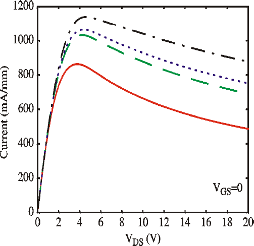
In Figure 3, a scaled device is examined. In this case, LG=0.5μm and LGS=LGD= 0.5μm. The contact resist-ances are held constant. A clear increase in output current accompanies the scaling and the trans-conductance has improved. The maximum current output has increased for the device with the best heatsinking (SiC substrate) from 812mA/mm to 1180mA/mm. For the device on sapphire a similar increase in the maximum current from 615mA/mm to 860mA/mm is seen. Clearly, with the increase in power the thermal impedance plays an even greater role.

Figure 3: Calculated current vs. voltage characteristics for a scaled HFET device on Al2O3 (solid), GaN (dashed), AlN (dotted), and SiC (dashed-dotted) are shown. The curves correspond to VGS=0V. VT=−4.0, Rc=0.5Ωmm, LGS=LG=LGD=0.5μm.
Conclusions
We have presented calculated current vs. voltage characteristics for a series of GaN-based HFETs on a variety of substrates, including sapphire, SiC, GaN, and AlN. Our device model is based on the field and temperature dependent electron velocity for GaN obtained by Monte Carlo transport simulations. The temperature is included self-consistently via a thermal impedance that takes into account the temperature dependence of the thermal conductivity of the substrate and the epitaxial materials. We demonstrate that the thermal properties of the substrate play a significant role in limiting the HFET performance under high-power conditions. In each of our simulations, the effects of improved heatsinking are shown to increase the DC output current and to decrease the negative output conductance observed for GaN HFETs.
In addition, our investigation included the effects of contact spacing as a second limiting factor for the device performance. By examining device geometries with the gate positioned closer to the source and a scaled device, it is shown that significant gains in the maximum current and transconductance can be achieved with these design improvements.
Acknowledgements
This work was supported in part by the National Science Foundation, the Office of Naval Research, the Minnesota Supercomputer Institute, and the National Research Council.