


Motivation
Electromagnetic devices are ubiquitous in our society, appearing in a variety of devices, including motors, memory/logic devices, and sensors/antennas. These magnetic devices presently create local magnetic fields by passing an electrical current through a conducting wire. The connection between a local magnetic field and current through a wire was accidentally discovered approximately 200 years ago, when Oersted found that a needle of a compass deflected when placed near a wire carrying electrical current. Today, we use this Oersted approach in a wide range of devices with some surpassing 90% efficiency. For example, electromagnetic motors use current-carrying coils to produce magnetic fields that drive permanent magnetics for moving items ranging from aircraft flaps to manipulating robotic platforms to propulsion of electric automobiles.
While Oersted’s approach works wonderfully in large-scale devices, it fails at small scales due to various issues. Specifically, the conversion efficiency in electromagnetic motors diminishes as the volume decreases below 1 cm3, due partly to resistive losses. While the efficiency drop-off is gradual, the efficiencies become insignificant at the nanoscale. For example, state-of-the-art magnetic memory (∼100 nm) using an electrical current is experimentally benchmarked at ∼0.0003% efficient and represents the primary obstacle for further memory miniaturization. Therefore, our society lacks an efficient approach to control magnetism at small scales (<1 mm). This magnetic control problem prevents the development of revolutionary micrometer or smaller size electromagnetic devices such as motors to drive blood cell size submarines, small sensors to measure the magnetic emission of brain activities, and miniature antenna systems to communicate from inside the body. Presently, these small-scale devices are relegated to the science fiction literature rather than appearing in engineering journal publications due to this efficiency problem. Thus, an immediate need exists to efficiently control magnetism at the small scale and continue the electromagnetic revolution initiated by Oersted’s discovery two centuries ago.
One approach to overcome this dilemma is to convert electrical to magnetic energy using magnetoelectric materials. Magnetoelectric materials are voltage driven rather than electrical current driven (Oersted approach) with negligible electrical resistive losses. Specifically, these dielectric materials require a small current and higher voltage as contrasted with Oersted’s high current and small voltage approach. These new magnetoelectric materials fall into three general categories—single-phase, charge-mediated, and strain-mediated materials. While each of these classes has specific benefits/drawbacks in terms of efficiency and operational characteristics, this issue of MRS Bulletin focuses on strain-mediated magnetoelectric materials, because they are considered the most mature magnetoelectric approach for near-term applications.
Strain-mediated magnetoelectric materials (Figure 1)Reference Eerenstein, Mathur and Scott1 are heterogeneous materials systems composed of piezoelectric and magnetoelastic materials that are mechanically coupled. An applied voltage creates a strain in the piezoelectric material (middle layer) that is transferred to the symmetrically attached magnetoelastic material in this illustrative description (Figure 1a). The strain induced in the magnetoelastic material alters the magnetic anisotropy, resulting in magnetic state control (i.e., magnetic spin rotation from Figure 1a–b) that generates external magnetic fields. Specifically, one might imagine a permanent magnet with north (N) and south (S) poles physically reoriented in space without having physically moved the structure, but by merely applying a voltage-induced strain.
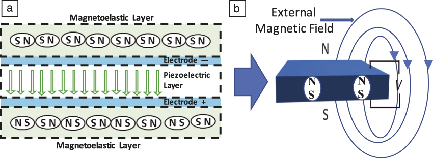
Figure 1. (a) Representative strain-mediated magnetoelectric containing a piezoelectric layer and two magnetoelastic layers with magnetization in-plane. (b) Following an applied voltage, the magnetization rotates by 90° to produce local magnetic fields in the air around the material (e.g., around the blue boxed region). Note: N, north; S, south; V, applied voltage.
One supporting factor for strain-mediated magnetoelectrics is that piezoelectric and magnetoelastic materials have been optimized over the last century, especially for sonar applications.Reference Wilson2 Thus, there is a relatively large selection of materials available to begin making and testing strain-mediated magnetoelectric devices. More importantly, the coupling coefficient (k 2) for existing piezoelectric materials (defines conversion of electrical to mechanical energy) and magnetoelastic materials (conversion of mechanical to magnetic energy) can each exceed 80%. Using the product of these two efficiencies, one finds that the theoretical energy transduced between the electrical to magnetic energy states approaches 64%.Reference Moffett, Clark, Wun-Fogle, Linberg, Teter and McLaughlin3,Reference Park and Shrout4 While this term represents an optimistic upper bound, it is still five orders of magnitude larger than presently available for magnetic memory bits. Therefore, strain-mediated magnetoelectric materials represent a revolutionary new (near-term) solution to the problem of efficiently controlling magnetism at the small scale.
Background
There are several literature reviewsReference Eerenstein, Mathur and Scott1,Reference Fiebig5 on this topic. In the 1820s, OerstedReference Ampere6 discovered that an electrical current passing through a wire produces a magnetic field (Figure 2). In the 1840s, JouleReference Joule7 discovered the direct conversion of magnetic energy into mechanical energy in magnetoelastic materials. Subsequently, in the 1880s,Reference Curie8 coupling between electrical energy and mechanical energy was discovered by the Curie brothers (piezoelectric materials). These latter two discoveries form the material basis of the strain-controlled magnetoelectrics we study today.
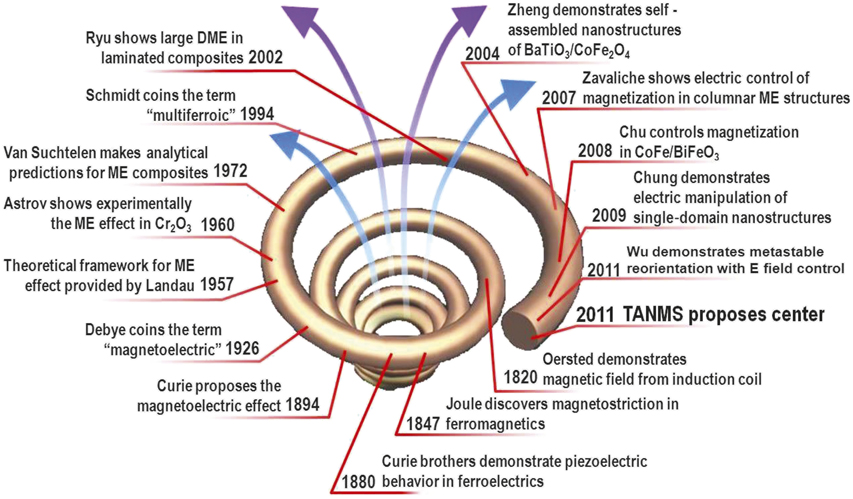
Figure 2. Illustration of the magnetoelectric history beginning with Oersted’s discovery in 1820 and continuing with the formation of the National Science Foundation Center for Transitional Applications of Nanoscale Multiferroic Systems (TANMS). Note: E, electric; ME, magnetoelectric; DME, direct magnetoelectric effect.
P. Curie made one of the first attempts (that failed) to find a single-phase magnetoelectric, arguably following up on his co-discovery of piezoelectric materials.Reference Curie9 Debye would coin the term “magnetoelectric” in the 1920sReference Debye10 that’s still in use today, but it would be another few decades until Landau’sReference Landau and Lifshitz11 analytical work confirmed its legitimacy. In the 1960s, Astrov and RadoReference Astrov12,Reference Rado and Folen13 experimentally discovered one of the first room-temperature magnetoelectric single-phase materials, Cr2O3. However, the coupling was too weak for it to be of practical interest. In 1972, Van SuchtelenReference Van Suchtelen14 suggested using a strain-mediated composite to increase the magnetoelectric response by mechanically coupling ferroelectric and ferromagnetic particles. In 1994, SchmidtReference Schmid15 coined the term “multiferroic” that has become synonymous to magnetoelectric with the added constraint that the material must possess both ferroelectric and ferromagnetic ordering. In 2002, Ryu et al.Reference Ryu, Priya, Uchino and Kim16 reported giant magnetoelectric coupling (i.e., a large transfer of energy from the magnetic state to the electrical state [direct magnetoelectric effect–DME]) in a laminated composite system consisting of lead zirconate titanate (PZT, Pb(ZrxTi1−x)O3) and Terfenol-D (Tb0.3Dy0.7Fe2). The name for the latter, developed at the Naval Ordnance Lab (NOL), is derived from terbium (Ter), iron (Fe), NOL, and dysprosium (D).
The vast majority of magnetoelectric research focuses on the DME, which is the generation of electric fields/energy in response to an applied magnetic field/energy. The DME is useful in sensor-based systems (e.g., magnetometers), but does not address the critical need in the commercial sector to generate magnetic fields at the small scale (e.g., similar to Oersted’s discovery). The latter is referred to as the converse magnetoelectric effect (CME). The CME is a more challenging problem due to the presence of domain walls in soft magnetoelastic materials that internally realign during mechanical loading, therefore inhibiting large external magnetic fields, even though the material’s internal magnetic state is modified. Thus, the reported CME response at large scales has been weaker than DMEReference Wu, Chang, Chung and Carman17 as well as less studied by the scientific community.Reference Wan, Liu, Wang and Nan18
Recognizing that the CME response represents a critical issue, researchers began focusing on structures to reduce or eliminate magnetic domain walls. Initial studies focused on thin-film magnetoelectrics (∼1-µm thickness).Reference Chung, Carman and Mohanchandra19–Reference Zhao, Zhao, Hunter, Suchoski, Gao, Mathews, Wuttig and Takeuchi23 Here, the number of magnetic domain walls could be reduced within the magnetoelastic material exhibiting a prominent in-plane (or out-of-plane) magnetization, utilizing magnetocrystalline anisotropy coupled with magnetic shape anisotropy. However, these large in-plane thin films still have closure domains (paths that prevent the magnetic field from exiting the material) at or near the edges of the film boundaries. ResearchersReference Kittel24 have known since the 1940s that soft magnetic materials fabricated at the nanoscale (∼100 nm) produce single magnetic domain structures (i.e., the complete elimination of domain walls).Reference Kittel24 Therefore, a handful of researchers began focusing on nanoscale (∼100-nm in-plane dimensions) magnetoelastic single magnetic domain structures for magnetoelectrics.
The integration of nanoscale magnetoelastic elements into magnetoelectric structures was initially explored in a materials-centric context in 2004. Zheng et al.Reference Zheng, Wang, Lofland, Ma, Mohaddes-Ardabili, Zhao, Salamanca-Riba, Shinde, Ogale, Bai and Viehland25 reported the fabrication of a self-assembled nanostructured BaTiO3-CoFe2O4 (piezoelectric-magnetoelastic). Zavaliche et al.Reference Zavaliche, Zhao, Zheng, Straub, Cruz, Yang, Hao and Ramesh26,Reference Zavaliche, Zheng, Mohaddes-Ardabili, Yang, Zhan, Shafer, Reilly, Chopdekar, Jia, Wright and Schlom27 reported in 2005, and subsequently in 2007, the electrical rearrangement of magnetization in epitaxial columnar nanostructures representing a major milestone in nanoscale magnetoelectrics. In 2009, researchers began focusing on evaluating individual single magnetic domain geometries (∼100-nm diameter nanodots) fabricated using electron-beam lithography. Films are initially deposited onto thin-film PZT and subsequently patterned into nanodots.Reference Chung, Keller and Carman28 The researchers found that the magnetic spin structure could be partially reoriented in magnetoelastic nanostructures, but the PZT-clamped thin film (i.e., on a silicon substrate) limited the spin reorientation.Reference Cui, Liang, Paisley, Sepulveda, Ihlefeld, Carman and Lynch29 Here, clamping refers to the fact that the relatively thick silicon substrate constrains PZT, thus limiting the elongation of PZT. Bur et al.Reference Bur, Wu, Hockel, Hsu, Kim, Chung, Wong, Wang and Carman30 conducted theoretical and experimental measurements to understand this problem and to determine the relationship between mechanical anisotropic strains necessary to reorient various magnetic single domains constrained by shape anisotropy. Wu et al.Reference Wu, Bur, Wong, Zhao, Lynch, Amiri, Wang and Carman31,Reference Wu, Zhao, Bao, Bur, Hockel, Wong, Mohanchandra, Lynch and Carman32 later reported that a magnetic single domain geometry (150 nm × 100 nm × 5 nm) could reorient both the spin state and the entire single domainReference Buzzi, Chopdekar, Hockel, Bur, Wu, Pilet, Warnicke, Carman, Heyderman and Nolting33 structure 90° to its original magnetization direction with an electric field.
Research space
To continue the magnetoelectric advancements accomplished over the last decade, researchers must begin improving the properties of the constituent materials as well as develop new modeling approaches (i.e., contrasted with sonar materials development). With regard to the material constituents, there are a number of piezoelectric materials and magnetoelastic materials that have been optimized for sonar applications. However, piezoelectrics have received substantially greater research effort as contrasted with magnetoelastic materials, and thus the area of magnetoelastic materials is considered a richer research area. Furthermore, both the piezoelectric and magnetoelastic materials are typically optimized for sonar based devices rather than other applications. For example, the magnetoelectric sensing community realized that magnetoelastic materials exhibiting large magnetostriction values (e.g., Terfenol-D) were inferior to amorphous magnetoelastic materials (FeGaB and FeCoSiBReference Lou, Insignares, Cai, Ziemer, Liu and Sun34) with lower magnetostrictions, but higher piezomagnetic coefficients. Furthermore, in the high-frequency space (e.g., antenna and spin waves operating at MHz and GHz frequencies), the conductive loss and magnetic loss in magnetoelastic materials become problematic, therefore, nonconducting materials that are soft, low-loss, and magnetostrictive (see work on magnetostrictive yttrium iron garnetsReference Quindeau, Avci, Liu, Sun, Mann, Tang, Onbasli, Bono, Voyles, Xu and Robinson35) need to be found. Regardless, a sufficient number of piezoelectric, and to a lesser degree magnetoelastic, materials are available to demonstrate proof-of-concept approaches with the understanding that additional material developments are needed to mature and move applications into the commercial sector.
In addition to materials research and discovery, modeling of these small-scale structures is critical to understand and foresee the complexities associated with the basic magnetoelectric operation. While modeling remains a challenge, this also offers unique opportunities to the research community. Strain-mediated magnetoelectric materials require mechanical analysis (to understand mechanical coupling), magnetic analysis (to understand spin reorientation), and electromagnetic radiation predictions. The three modeling areas are represented by governing equations defined by Newton’s equations of elastodynamics, Landau–Lifshitz–Gilbert (LLG) equations of micromagnetics, and Maxwell’s equations of electromagnetism. While each of these three governing equations has received considerable research attention during the last century, few if any studies exist on solving the coupled partial differential equations when all mathematical constructs are fully coupled and thus required for accurate representation.Reference Liang, Keller, Sepulveda, Bur, Sun, Wetzlar and Carman36–Reference Keller and Carman38 Each set of equations has been traditionally solved by the mechanical engineering, physics, or electrical engineering communities uncoupled from the other systems of equations. While the study of piezoelectric and magnetoelastic materials in sonar systems utilizes the electrostatic approximation of Maxwell’s equations with a linearization of the constitutive equations in Newton’s equations, these oversimplifications are inappropriate for understanding and predicting the dynamic response of magnetoelectrics at the small scale. To reinforce this argument, one needs to consider the state equations utilized by the magnetic memory community (LLG micromagnetics) to support the notion that classical piezoelectric and magnetoelastic approaches are inadequate for understanding small-scale strain mediated magnetoelectric dynamics. Therefore, a unique opportunity exists for the modeling community working at the interfaces between mechanics–magnetism, magnetism–electromagnetics, and mechanics–electromagnetics to solve new problems as well as to unveil new discoveries.Reference Hu, Yang, Momeni, Cheng, Chen, Lei, Zhang, Trolier-McKinstry, Gopalan, Carman, Nan and Chen39,Reference Chen, Barra, Mal, Carman and Sepulveda40 This new analytical push could yield a wealth of original information if a sufficient number of researchers begin exploring this research area.
Application space
Efficiently controlling magnetism at small scales provides a number of possible revolutionary applications suggested by science fiction novels. These miniature devices include elements such as efficient magnetic memory/logic devices, small electromagnetic motors, human T-cell manipulation, magnetic sensors, and electrically small magnetic-based antennas. In the memory and logic arena, the potential to reduce energy consumption by several orders of magnitude provides unique opportunities, including resolution of the heat-generation problem arising during the writing process, as the demand for packing more bits of memory into smaller space increases.
Biological cell manipulation requires the ability to individually control a cell attached to a magnetic particle. The magnetic manipulation of cells with bulk devices has seen considerable growth during the last decade,Reference Talasaz, Powell, Huber, Berbee, Roh, Yu, Xiao, Davis, Pease, Mindrinos and Jeffrey41,Reference Tanase, Biais and Sheetz42 however, few efforts exist on attempts to control individual cells (i.e., lack of local [micrometer] magnetic control). Individual cell manipulation allows for the selection of T-cells that are optimized to fight individual diseases such as specific forms of cancer. For antenna platforms, the magnetoelectric approach offers a new paradigm to develop a magnetic current-based electrically small antenna using voltage control. This particular advancement provides a new approach to decrease antenna size due to the relatively slower mechanical wave speed associated (i.e., 103 m/s) with magnetoelectric materials contrasted with the light speed (i.e., 108 m/s) in conventional Hertz-based antennas.Reference Yao, Wang, Keller and Carman37,Reference Keller and Carman38 This should come as no surprise to the magnetic community where magnetic spin waves propagate at speeds close to mechanical waves rather than electromagnetic waves. These strain-mediated magnetoelectric antennas thus offer a new paradigm branching away from the Oersted approach Hertz originally utilized in the first dipole antenna and moving toward voltage driven strain mediated magnetoelectrics.Reference Nan, Lin, Gao, Matyushov, Yu, Chen, Sun, Wei, Wang, Li, Wang, Belkessam, Guo, Chen, Zhou, Qian, Hui, Rinaldi, McConney, Howe, Hu, Jones, Brown and Sun43
One of the more exciting areas of study is the development of micrometer-sized electromagnetic motors. Large-scale motors are employed widely in applications ranging from controlling aircraft flaps to propulsion systems in electric vehicles. Electromagnetic motors consist of two main components, in other words, a rotor (permanent magnetic field) and a stator (controlling the magnetic field). The new magnetoelectric motors under development have direct operational similarities to macroscale Oersted motors. The moveable rotor remains a magnetic material susceptible to an external magnetic field. For the stator, the copper coil is replaced with a voltage-driven magnetoelectric material (i.e., voltage control of magnetic state).
Figure 3a shows an illustration of a representative stator with a magnetoelastic ring deposited onto a piezoelectric PZT thin film. Electrodes sit around the magnetoelastic periphery to apply voltage-induced directional strain to the magnetoelastic ring.Reference Liang, Sepulveda, Hoff, Keller and Carman44 Also shown in Figure 3b are experimental data demonstrating how the magnetoelastic ring’s magnetic orientation is rotated with the application of an electric field.Reference Sohn, Liang, Nowakowski, Hwang, Han, Bokor, Carman and Candler45 This provides a new type of stator platform to control the local magnetization and move the rotor with an applied voltage. Figure 3c shows an artist’s rendition of a white bar rotor magnet placed on top of the magnetoelectric stator, which rotates as a voltage is applied to the piezoelectric/ferroelectric (i.e., voltage-driven electromagnetic motor with mechanical output). This rotation has already been experimentally achieved with particle-based rotors,Reference Sohn, Nowakowski, Liang, Hockel, Wetzlar, Keller, McLellan, Marcus, Doran, Young, Kläui, Carman, Bokor and Candler46 as contrasted with a rod rotor illustrated in Figure 3c. If one were to imagine a future miniature robotic submarine (Figure 3d) one might contemplate a propulsion system based on magnetoelectric materials using flagella-type propellers. Such a submarine could be used in a biomedical application where the submarine traverses through the vascular system while recording data with an efficient magnetoelectric memory to reduce battery drain. The information could be transmitted to the external world using a small magnetoelectric antenna operating at the Medical Implant Communication Standard of 401–406 MHz frequency.Reference Islam and Yuce47 The field of strain-mediated magnetoelectrics thus offers substantial promise to produce devices previously relegated to the annals of science fiction novels as engineering moves closer to small-scale robotic-based platforms that do not presently exist.
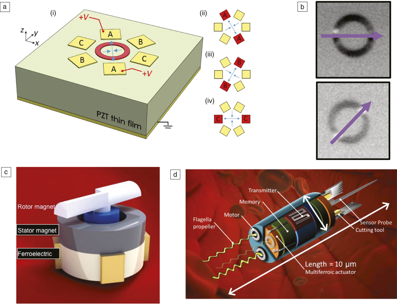
Figure 3. (a, d) The illustration shows a schematic of a red magnetoelastic ring on top of a piezoelectric thin film surrounded by electrodes to control the voltage-induced strain. (i) The blue arrows within the magnetoelastic ring represent the strain direction generated when a voltage (V) is applied. (ii–iv) The red boxes represent the electrodes to which the voltage is applied as strain, and magnetization (blue arrows) rotate around the periphery of the disk. (b) The photoemission electron microscope images show an experimental demonstration that the voltage-induced strain reorients the magnetization state in a ∼1-µm diameter magnetoelastic ring with the arrows representing magnetic reorientation between the states. Illustrations of (c) an electromagnetic motor and (d) a ∼20-µm diameter submarine with magnetoelectric propulsion, data storage, and communications. Note: PZT, lead zirconate titanate.
In this issue
During the last decade, several critical scientific and engineering underpinnings have been developed, supporting the premise that we are on the verge of a major new revolution in magnetoelectrics. This issue contains five articles that were selected based on the work achieved in the magnetoelectric area as well as the potential each has for advancing the field. These articles are representative of the quality and the scientific importance of ongoing research in the field rather than representing the entire breadth of magnetoelectric discoveries achieved during the last decade.
In their article in this issue, Viehland et al. focus on a review of work conducted in the study of static to quasi-static magnetic field sensing.Reference Viehland, Wuttig, McCord and Quandt48 This general topical area represents the seed application contributing to the field’s exponential growth during the beginning of the 21st century. A number of researchers around the world have developed significant advancements, such as increasing the magnetic sensitivity of these small-scale magnetoelectric sensors to approach that of large superconducting quantum interference devices. Presently, these groups are on the verge of delivering a small-scale extremely sensitive magnetometer to the medical community for measuring brain activity (magnetoencephalography).
Next, the Lin et al. article extends the science explained in the Viehland et al. article to measuring/producing magnetic field variation in the dynamic range (i.e., at MHz and GHz frequencies), rather than using relatively stationary applications of magnetic fields/measurements.Reference Lin, Page, McConney, Jones, Howe and Sun49 This article also describes the transmission of magnetic information in the dynamic range (CME) as contrasted to the focus of magnetic field measurements (DME) of the previous article. This high-frequency area is rich for basic scientific studies (electrically small antennas using magnetic current) and engineering applications (implantable antennas) with the authors reporting the first high-frequency demonstration of a magnetoelectric antenna. The 100-µm scale antenna is capable of both receiving (i.e., DME similarities with magnetometer) and transmitting (CME) at GHz frequencies.
The Xu and Nan article focuses on modeling advancements accomplished in magnetoelectrics at length scales ranging from atomistic to continuum bulk levels.Reference Xu and Nan50 These models include descriptions of phase-field methods at the mesoscale, molecular dynamics at the atomic scale, and first-principles calculations at the electronic scale. These modeling efforts are critical because the control of magnetic states with an applied voltage represents a coupled nonlinear multiscale multiphysics problem. Therefore, using a “make it and test it” approach to resolve problems or develop new devices requires extensive time, so these new complex modeling approaches are necessary to quickly understand and guide the research and development efforts.
In their article, Domann et al. review the progress on voltage-induced strain to produce magnetic changes in magnetic thin films and nanoscale single magnetic domain elements.Reference Domann, Wu, Chung and Carman51 The researchers highlight several characteristics enabling small, fast, energy-efficient technologies (i.e., contrasted with the Oersted approach) for a wide range of applications, including data storage, transmission, and processing of information. Here, experimental demonstrations are presented to guide the reader toward future applications as well as demonstrate that the field is building upon firm scientific evidence.
Finally, Foerster et al. discuss our understanding of the dynamic response of mechanical waves interacting with magnetic spin waves.Reference Foerster, Aballe, Hernàndez and Macià52 This more fundamental research description provides a pathway to explore new dynamic coupling phenomenon while articulating the complexities associated with making nanometer- to micrometer-sized scale measurements. This research has important ramifications in the intersection between mechanical waves (velocity ∼ km/s), magnetic spin waves (velocity ∼km/s), and electromagnetic waves (velocity ∼105 km/s).
Conclusion
The articles in this issue are intended to motivate the reader to pursue research in this expanding magnetoelectric area (i.e., control of magnetism at the small scale). Here, it is important to note that the articles are representative of the excellent ongoing work rather than covering the entire magnetoelectric area (e.g., single-phase magnetoelectrics, charge-mediated magnetoelectrics, materials development). The field remains in a growth phase and has yet to reach critical mass where there is a clear focus on efficiently controlling magnetism at the small scale. The authors of this issue are hopeful that the scientific community uses this general information as a problem statement to help continue or initiate research efforts. In general, substantial opportunities exist in the nanometer to micrometer scale for discovering new materials, developing innovative modeling approaches, and generating new devices. The application space is considered speculative, because as of today, the community lacks an efficient approach to control magnetism at the small scale. However, the magnetoelectric area offers an extraordinarily rich area for fundamental research with the extended promise of turning science fiction into reality in the relatively near future.
Acknowledgment
This material is based upon work supported by the National Science Foundation under Cooperative Agreement Award EEC-1160504.

Gregory P. Carman is the director of the National Science Foundation Engineering Research Center Translational Applications of Nanoscale Multiferroic Material Systems, and is Co-executive Director of the Center for Advanced Surgical and Interventional Technology in the Department of Surgery at the University of California, Los Angeles (UCLA). He joined the Mechanical and Aerospace Engineering Department at UCLA in 1991. He has served as chairman for the Adaptive Structures and Material Systems of the ASME (2000–2002), and is an associate editor for the Journal of Intelligent Material Systems and Structures and Smart Materials and Structures. He was awarded the Northrop Grumman Young Faculty Award in 1995 and three best paper awards from the ASME in 1996, 2001, and 2007. In 2015, SPIE honored him with the SSM Lifetime Achievement Award, and in 2016, he was invited to be the Distinguished Lecturer for the IEEE Magnetic Society. His research interests focus on analytical modeling, fabrication, and testing of magnetoelectric materials and developing devices for medical applications. Carman can be reached by email at carman@seas.ucla.edu.

Nian Sun is the founder and chief technical advisor of Winchester Technologies, LLC, and a professor in the Electrical and Computer Engineering Department, Director of the W.M. Keck Laboratory for Integrated Ferroics, Northeastern University, and Thrust Leader of 2D Multiferroics in the National Science Foundation Engineering Research Center Transitional Applications of Nanoscale Multiferroic Systems. He received his PhD degree from Stanford University. He is an editor of the journals Sensors and IEEE Transactions on Magnetics. He is a Fellow of the Institute of Physics and the Institution of Engineering and Technology. Prior to joining Northeastern University, he was a scientist at IBM and Hitachi Global Storage Technologies. He was the recipient of the NSF CAREER Award, ONR Young Investigator Award, and the Søren Buus Outstanding Research Award. He has more than 240 publications, 20 patents, and patent applications. Sun can be reached by email at n.sun@northeastern.edu.


