


Introduction
Polycrystalline materials are ubiquitous in technological applications. An ideal crystal structure can be fully defined with a small number of parameters: the three vectors defining its unit cell, and the position and species of each atom inside the unit cell (Borchardt-Ott, Reference Borchardt-Ott2011). To fully describe crystalline materials in the real world however, we require a description of both the crystal lattice, and all defects present in a given material. These include point defects such as dopants, vacancies, or interstitials (Dederichs et al., Reference Dederichs, Lehmann, Schober, Scholz and Zeller1978), line defects such as dislocations (LeSar, Reference LeSar2014), planar defects including internal boundaries and surfaces (Tang et al., Reference Tang, Carter and Cannon2006), and volume defects such as precipitates (Kleiven & Akola, Reference Kleiven and Akola2020). Strain fields in the surrounding material can be induced by each of these defects, or generated by the boundary or growth conditions of the material such as in thin film stresses (Janssen, Reference Janssen2007). One large subset of crystalline materials are polycrystalline phases, which consist of many small crystalline grains, arranged in either a random or organized fashion. Many material properties such as mechanical strength (Thompson, Reference Thompson2000), optical response (Park et al., Reference Park, Park, Lee, So, Kim, Jeong, Han, Wolf, Lee, Yoo and Tae-Woo2019; Londoño-Calderon et al., Reference Londoño-Calderon, Williams, Schneider, Savitzky, Ophus, Ma, Zhu and Pettes2021), or th\ermal or electrical conductivity (Castro-Méndez et al., Reference Castro-Méndez, Hidalgo and Correa-Baena2019) are strongly modulated by the density and orientation of the boundaries between crystalline grains (Thompson & Carel, Reference Thompson and Carel1995). Thus, characterizing the orientation of polycrystalline grains is essential to understanding these materials.
The two primary tools used to study the orientation of polycrystalline materials are electron backscatter diffraction (EBSD) in scanning electron microscopy (SEM), and transmission electron microscopy (TEM). EBSD can measure the orientation of crystalline grains with very high accuracy, but has limited resolution and is primarily sensitive to the surface of materials (Humphreys, Reference Humphreys2001; Wright et al., Reference Wright, Nowell and Field2011, Reference Wright, Nowell, Lindeman, Camus, De Graef and Jackson2015). Alternatively, we can directly measure the atomic-scale structure and therefore the orientation of polycrystalline grains, either by using plane wave imaging in TEM (Li et al., Reference Li, Jin, Zhou and Lu2020), or by focusing the probe down to subatomic dimensions and scanning over the sample surface in scanning TEM (STEM; Peter et al., Reference Peter, Frolov, Duarte, Hadian, Ophus, Kirchlechner, Liebscher and Dehm2018). This is possible due to the widespread deployment of aberration correction for both TEM and STEM instruments (Linck et al., Reference Linck, Hartel, Uhlemann, Kahl, Müller, Zach, Haider, Niestadt, Bischoff, Biskupek, Lee, Lehnert, Börrnert, Rose and Kaiser2016; Ramasse, Reference Ramasse2017). Atomic resolution imaging, however, strictly limits the achievable field-of-view, and requires relatively thin samples, and thus is primarily suited for measuring polycrystalline grain orientations of 2D materials (Ophus et al., Reference Ophus, Shekhawat, Rasool and Zettl2015; Qi et al., Reference Qi, Sahabudeen, Liang, Položij, Addicoat, Gorelik, Hambsch, Mundszinger, Park, Lotsch, Mannsfeld, Zheng, Dong, Heine, Feng and Kaiser2020).
Another approach to orientation mapping in TEM is to use diffraction space measurements. For crystalline materials, diffraction patterns will contain Bragg spots with spacing inversely proportional to the spacing of atomic planes which are approximately perpendicular to the beam direction (described by both the Laue condition and Bragg equations; Fultz & Howe, Reference Fultz and Howe2012). To generate a spatially resolved orientation map, we can focus a STEM probe down to dimensions of 0.5–50 nm, scan it over the sample surface, and record the diffraction pattern for each probe position. This technique is referred to as nanobeam electron diffraction (NBED; Ozdol et al., Reference Ozdol, Gammer, Jin, Ercius, Ophus, Ciston and Minor2015), scanning electron nanobeam diffraction (SEND; Tao et al., Reference Tao, Niebieskikwiat, Varela, Luo, Schofield, Zhu, Salamon, Zuo, Pantelides and Pennycook2009), or four-dimensional scanning transmission electron microscopy (4D-STEM) (we choose this nomenclature for this text) due to the 4D shape of the collected data (Bustillo et al., Reference Bustillo, Zeltmann, Chen, Donohue, Ciston, Ophus and Minor2021). 4D-STEM experiments are increasingly enabled by fast direct electron detectors, as these cameras allow for much faster recording and much larger fields of view (Ophus, Reference Ophus2019; Nord et al., Reference Nord, Webster, Paton, McVitie, McGrouther, MacLaren and Paterson2020; Paterson et al., Reference Paterson, Webster, Ross, Paton, Macgregor, McGrouther, MacLaren and Nord2020).
By performing template matching of diffraction pattern libraries on 4D-STEM datasets, we can map the orientation of all crystalline grains with sufficient diffraction signal. This method is usually named automated crystal orientation mapping (ACOM) and has been used by many authors in materials science studies (Zaefferer & Schwarzer, Reference Zaefferer and Schwarzer1994; Rauch & Dupuy, Reference Rauch and Dupuy2005; Wu & Zaefferer, Reference Wu and Zaefferer2009; Kobler et al., Reference Kobler, Kashiwar, Hahn and Kübel2013; Londoño-Calderon et al., Reference Londoño-Calderon, Williams, Ophus and Pettes2020; MacLaren et al., Reference MacLaren, Frutos-Myro, McGrouther, McFadzean, Weiss, Cosart, Portillo, Robins, Nicolopoulos, Del Busto and Skogeby2020; Jeong et al., Reference Jeong, Cautaerts, Dehm and Liebscher2021; Zuo & Zhu, Reference Zuo and Zhu2021). ACOM experiments in 4D-STEM are highly flexible; two recent examples include Lang et al. (Reference Lang, Taylor, Pratt, Nenoff and Hattar2021) implementing ACOM measurements in liquid cell experiments, and Wu et al. (Reference Wu, Harreiss, Ophus and Spiecker2021) adapting the ACOM method to a scanning confocal electron diffraction (SCED) experimental configuration. ACOM is also routinely combined with precession electron diffraction, where the STEM beam is continually rotated around a cone incident onto the sample, in order to excite more diffraction spots and thus produce more interpretable diffraction patterns (Rauch et al., Reference Rauch, Portillo, Nicolopoulos, Bultreys, Rouvimov and Moeck2010; Brunetti et al., Reference Brunetti, Robert, Bayle-Guillemaud, Rouviere, Rauch, Martin, Colin, Bertin and Cayron2011; Moeck et al., Reference Moeck, Rouvimov, Rauch, Véron, Kirmse, Häusler, Neumann, Bultreys, Maniette and Nicolopoulos2011; Eggeman et al., Reference Eggeman, Krakow and Midgley2015). Recently, Mehta et al. (Reference Mehta, Gauquelin, Nord, Orekhov, Bender, Cerbu, Verbeeck and Vandervorst2020) have combined simulations with machine learning segmentation to map orientations of 2D materials, and Yuan et al. (Reference Yuan, Zhang, He and Zuo2021) have used machine learning methods to improve the resolution and sensitivity of orientation maps by training on simulated data. For more information, Zaefferer (Reference Zaefferer2011) has provided a review of ACOM methods in SEM and TEM.
In this study, we introduce a new sparse correlation framework for fast calculation of orientation maps from 4D-STEM datasets. Our method is based on template matching of diffraction patterns along only the populated radial bands of a reference crystal's reciprocal lattice, and uses direct sampling of the first two Euler angles (which, in the convention we have adopted, correspond to the zone axis), and a fast Fourier transform correlation step to solve for the final Euler angle (in our convention, the in-plane rotation of the pattern). We test our method on both kinematical calculations, and simulated diffraction experiments incorporating dynamical diffraction. Finally, we generate orientation maps of polycrystalline AuAgPd helically twisted nanowires, and use clustering to segment the polycrystalline structure, and map the shared (111) twin planes of adjacent grains.
Methods
Overview
The problem we are solving is to identify the relative orientation between a given diffraction pattern measurement and a parent reference crystal. We solve this problem with three steps:
1. First, we generate a diffraction pattern library which covers all unique crystal orientations using kinematical simulation. This library, stored in a sparse polar coordinate representation $P$, is called an “orientation plan.”
2. We find all diffracted spots/disks in each diffraction pattern, and convert them into the same sparse polar coordinate representation
$X$.3. We determine the best fit orientation(s) by finding the maximum value(s) of the correlation
$C$ between the diffraction patterns and the orientation plan.


All of the previously discussed ACOM implementations work in essentially the same way, that is, by precomputing the diffraction library in some form, and then comparing each diffraction pattern to this library using a cost function based on some form of correlation. Performing template matching directly on diffraction patterns, which may contain millions of pixels, against a library of similarly sized patterns, is computationally expensive. However, the underlying information we are interested in, that is, the projected lattice in the pattern, is typically composed of at most a few dozen non-zero points. Our sparse correlation method involves reducing the diffraction patterns to a simpler representation where the correlation can be evaluated rapidly, by first detecting the positions of the Bragg disks in the pattern, then segmenting the data into radial bands, and only evaluating the correlation in the populated bands.
The primary advances of this paper are listed as follows: (1) We use Fourier transforms along the annular direction in polar coordinates for both the diffraction library and diffraction patterns to efficiently solve for the in-plane image rotation. For a full polar coordinate transform, only a small number of radial bins will contain reciprocal lattice points, and thus, the output is sparse along the radial direction. We utilize this sparsity by only evaluating the polar coordinate correlations on radial shells that contain reciprocal lattice points of the reference structure, making the calculations much faster. (2) We give users fine-grained control over the relative weighting of diffraction peak radii and intensities in the correlation calculation, as well defining a kernel size which can be increased to allow more pattern distortion, or decreased to reduce the chance of false positive signals from grains with close orientations. (3) We automatically determine the symmetry-reduced range of allowed zone axes from the input crystal. (4) We provide all methods and codes as an open source implementation for the community to freely use and modify. Below we detail each of the steps for our orientation matching algorithm, and their required input calculations.
Structure Factor Calculations
The structure factors of a given crystalline material are defined as the complex coefficients of the Fourier transform of an infinite crystal (Spence, Reference Spence1993). We require these coefficients in order to simulate kinematical diffraction patterns, and thus, we briefly outline their calculation procedure here.
First, we define the reference crystal structure. This structure consists of two components, the first being its unit cell defined by its lattice vectors  ${\boldsymbol a}$, ${\boldsymbol b}$, and ${\boldsymbol c}$ composed of positions in ${\boldsymbol r} = ( x,\; y,\; z)$, the 3D real space coordinate system. The second component of a crystal structure is an array with dimensions $[ N,\; 4]$ containing the fractional atomic positions ${\boldsymbol p}_n = ( p_{{\boldsymbol a}},\; p_{{\boldsymbol b}},\; p_{{\boldsymbol c}}) _n$ and atomic number $Z_n$, for the $n$th index of $N$ total atoms in the unit cell. Together these positions and atomic numbers are referred to as the atomic basis. Because ${\boldsymbol p}_n$ is given in terms of the lattice vectors, all fractional positions have values inside the range $[ 0,\; 1)$. The unit cell and real space Cartesian coordinates of the (face centered cubic) fcc Au structure are plotted in Figure 1a.
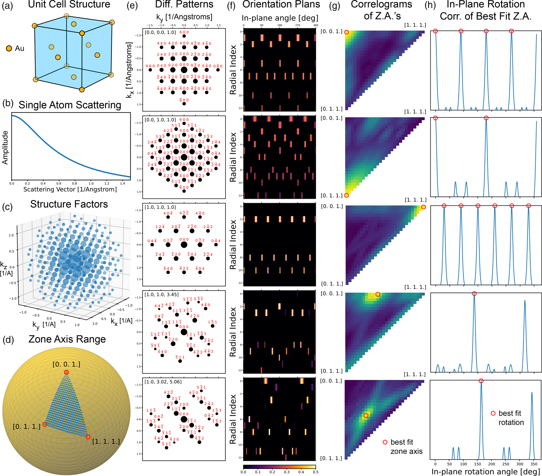
Fig. 1. ACOM using correlation matching in py4DSTEM. (a) Structure of fcc Au. (b) Atomic scattering factor of Au. (c) Structure factors for fcc Au. (d) Zone axes included in orientation plan. (e) Diffraction patterns for various orientations, and (f) corresponding orientation plan slices. (g) Correlogram maxima for each pattern in (e) as a function of zone axis, and (h) corresponding in-plane rotation correlation. Highest correlation scores are shown in (g) and (h) using red circles.
All subsequent calculations are performed in reciprocal space (also known as Fourier space or diffraction space). Thus, the next step is to compute the reciprocal lattice vectors, defined by Gibbs (Reference Gibbs1884)
 $$\eqalign{{\boldsymbol a}^{\ast } & = {{\boldsymbol b} \times {\boldsymbol c}\over {\boldsymbol a} \cdot [ {\boldsymbol b} \times {\boldsymbol c}] } = {{\boldsymbol b} \times {\boldsymbol c}\over \Omega}, \cr {\boldsymbol b}^{\ast } & = {{\boldsymbol c} \times {\boldsymbol a}\over {\boldsymbol b} \cdot [ {\boldsymbol c} \times {\boldsymbol a}] } = {{\boldsymbol c} \times {\boldsymbol a}\over \Omega}, \cr {\boldsymbol c}^{\ast } & = {{\boldsymbol a} \times {\boldsymbol b}\over {\boldsymbol c} \cdot [ {\boldsymbol a} \times {\boldsymbol b}] } = {{\boldsymbol a} \times {\boldsymbol b}\over \Omega},\; }$$
where  $\times$ represents the vector cross product and $\Omega$ is the unit cell volume in real space. Note that this definition does not include factors of $2\pi$, and therefore, all reciprocal coordinates have spatial frequency units.
Next, we calculate the position of all reciprocal lattice points required for our kinematical diffraction calculation, given by
 $${\boldsymbol g}_{hkl} = h {\boldsymbol a}^{\ast } + k {\boldsymbol b}^{\ast } + l {\boldsymbol c}^{\ast },\; $$
where  $h$,
$h$,  $k$, and $l$ are integers representing the reciprocal lattice index points corresponding to the Miller indices $( h,\; k,\; l)$. We include only points where $\vert {\boldsymbol q}_{hkl}\vert < k_{{\rm max}}$, where ${\boldsymbol q} = ( q_x,\; q_y,\; q_z)$ are the 3D coordinates in reciprocal space, that is those which fall inside a sphere given by the maximum scattering vector $k_{{\rm max}}$. To find all reciprocal lattice coordinates, we first determine the shortest vector given by linear combinations of $( {\boldsymbol a}^{\ast },\; {\boldsymbol b}^{\ast },\; {\boldsymbol c}^{\ast })$, and divide $k_{{\rm max}}$ by this vector length to give the range for $( h,\; k,\; l)$. We then tile $( h,\; k,\; l)$ in both the positive and negative directions up to this value, and then remove all points with vector lengths larger than $k_{{\rm max}}$.
The reciprocal lattice defined above represents all possible coordinates where the structure factor coefficients  $V_g( {\boldsymbol q})$ could be non-zero. The structure factor coefficients depend only the atomic basis and are given by
 $$F_{hkl} = {1\over \Omega} \sum_{n = 1}^{N} f_n( \vert {\boldsymbol g}_{hkl}\vert ) \exp[ -2 \pi {{\rm i}} ( h,\; k,\; l) \cdot {\boldsymbol p}_n ] ,\; $$
where  $f_n$ are the the single-atom scattering factors for the $n$th atom, which describe the scattering amplitude for a single atom isolated in space. There are multiple ways to parameterize $f_n$, but here we have chosen to use the factors defined by Lobato & Van Dyck (Reference Lobato and Van Dyck2014) which are implemented in py4DSTEM. Figure 1b shows the atomic scattering factor for an Au atom.
We have now defined all structure factor coefficients for a perfect infinite crystal as
 $$V_g( {\boldsymbol q}) = \left\{\matrix{ F_{hkl}, \hfill & \hbox{if } {\boldsymbol q} = {\boldsymbol g}_{hkl}, \hfill \cr 0, \hfill & \hbox{otherwise}. \hfill }\right.$$
Figure 1c shows the structure factors of fcc Au, where the marker size denotes the intensity (magnitude squared) of the  $F_{hkl}$ values.
Calculation of Kinematical Diffraction Patterns
Here, we briefly review the theory of kinematical diffraction of finite crystals, following De Graef (Reference De Graef2003). We can fully describe an electron plane wave by its wavevector  ${\boldsymbol k}$, which points in the direction of the electron beam and has a length given by $\vert {\boldsymbol k}\vert = 1/\lambda$, where $\lambda$ is the (relativistically corrected) electron wavelength. Bragg diffraction of the electron wave along a direction ${\boldsymbol k}'$ occurs when electrons scatter from equally spaced planes in the crystal, described in reciprocal space as
 $${\boldsymbol k}' = {\boldsymbol k} + {\boldsymbol g}_{hkl}.$$
For elastic scattering,  ${\boldsymbol k}'$ has the same length as ${\boldsymbol k}$, and so scattering can only occur along the spherical surface known as the Ewald sphere construction (Ewald, Reference Ewald1921). For a perfect infinite crystal, scattering will seemingly almost never happen since it requires intersection of the Ewald sphere with the infinitesimally small points of the reciprocal lattice vectors. However, real samples have finite dimensions, and thus, in reciprocal space, their lattice points will be convolved by a shape factor $D( {\boldsymbol q})$. Therefore, diffraction can still occur, as long as equation (5) is approximately satisfied.
If the sample foil is tilted an angle  $\alpha$ away from the beam direction, the vector between a reciprocal lattice point ${\boldsymbol g}$ and its closest point on the Ewald sphere has a length equal to
 $$s_{{\boldsymbol g}} = {-{\boldsymbol g} \cdot( 2 {\boldsymbol k} + {\boldsymbol g}) \over 2 \vert {\boldsymbol k} + {\boldsymbol g} \vert \cos( \alpha) }.$$
The  $s_{{\boldsymbol g}}$ term is known as the excitation error of a given reciprocal lattice point ${\boldsymbol g}$. When the excitation error $s_{{\boldsymbol g}} = 0$, the Bragg condition is exactly satisfied. When the length of $s_{{\boldsymbol g}}$ is on the same scale as the extent of the shape factor, the Bragg condition is approximately satisfied.
A typical TEM sample can be approximately described as a slab or foil which is infinite in two dimensions, and with some thickness  $t$ along the normal direction. The shape function of such a sample is equal to
 $$D( q_z) = {\sin( \pi q_z t) \over \pi q_z}.$$
Because this expression is convolved with each reciprocal lattice point, we can replace  $q_z$ with the distance between the Ewald sphere and the reciprocal lattice point. For the orientation mapping application considered in this paper, we assume that $\alpha = 0$, and that the sample thickness $t$ is unknown. Instead, we replace equation (7) with the approximation
 $$D( q_z) = \exp\left(-{{q_z}^{2}\over 2 \sigma^{2}}\right),\; $$
where  $\sigma$ represents the excitation error tolerance for a given diffraction spot to be included. We chose this expression for the shape function because it decreases monotonically with increasing distance between the diffraction spot and the Ewald sphere $q_z$, and produces smooth output correlograms.
To calculate a kinematic diffraction pattern for a given orientation  ${\boldsymbol w}$, we loop through all reciprocal lattice points and use equation (6) to calculate the excitation errors. The intensity of each diffraction spot is given by the intensity of the structure factor $\vert F_{hkl}\vert ^{2}$, reduced by a factor defined by either equation (7) or equation (8). We define the position of the diffraction spots in the imaging plane by finding two vectors perpendicular to the beam direction, and projecting the diffraction vectors $q$ into this plane. The result is the intensity of each spot $I_m$, and its two spatial coordinates $( q_{m_x},\; q_{m_y})$, or alternatively their polar coordinates $q_m = \sqrt {{q_{m_x}}^{2} + {q_{m_y}}^{2}}$ and $\gamma _m =$ arctan2 $( q_{m_y},\; q_{m_x})$. Note that the in-plane rotation angle is arbitrarily defined for kinematical calculations in the forward direction. The resulting diffraction patterns are defined by the list of $M$ Bragg peaks, each defined by a triplet $( q_{m_x},\; q_{m_y},\; I_m)$ in Cartesian or $( q_m,\; \gamma _m ,\; I_m)$ in polar coordinates.
Figure 1e shows diffraction patterns for fcc Au, along five different zone axes (orientation directions). Each pattern includes Bragg spots out to a maximum scattering angle of  $k_{{\rm max}} = 1.5 \, {\ring{\rm A} }^{-1}$, and each spot is labeled by the $( hkl)$ indices. The marker size shown for each spot scales with the amplitude of each spot's structure factor, decreased by equation (8) using $\sigma = 0.02 \, {\ring{\rm A} }^{-1}$.
Generation of an Orientation Plan
The orientation of a crystal can be uniquely defined by a  $[ 3 \times 3]$-size matrix $\mathop_{\raise2pt{\boldsymbol m}}^{\hskip-0.6pt\leftrightarrow}$, which rotates vectors ${\boldsymbol d}_0$ in the sample coordinate system to vectors ${\boldsymbol d}$ in the parent crystal coordinate system
 $$\eqalign{\left[\matrix{d_x \cr d_y \cr d_z }\right]& = \left[\matrix{ u_x & v_x & w_x \cr u_y & v_y & w_y \cr u_z & v_z & w_z }\right]\left[\matrix{d_{0_x} \cr d_{0_y} \cr d_{0_z} }\right]\cr {\boldsymbol d} & = \raise4pt{\mathop_{\vskip-2pt{\boldsymbol m}}^{\hskip-0.6pt{\raise-2pt\leftrightarrow}}} \, {\boldsymbol d}_0,\; }$$
where the first two columns of  $\mathop_{\raise2pt{\boldsymbol m}}^{\hskip-0.6pt\leftrightarrow}$ given by ${\boldsymbol u}$ and ${\boldsymbol v}$ represent the orientation of the in-plane $x$- and $y$-axis directions of the parent crystal coordinate system, respectively, and the third column ${\boldsymbol w}$ defines the zone axis or out-plane-direction. The orientation matrix can be defined in many different ways, but we have chosen to use a $Z-X-Z$ Euler angle scheme (Rowenhorst et al., Reference Rowenhorst, Rollett, Rohrer, Groeber, Jackson, Konijnenberg and De Graef2015), defined as
 $${\raise4pt{\mathop_{\vskip-2pt{\boldsymbol m}}^{\hskip-0.6pt{\raise-2pt\leftrightarrow}}}} = \left[\matrix{ C_1 & -S_1 & 0 \cr S_1 & C_1 & 0 \cr 0 & 0 & 1 }\right]\left[\matrix{ 1 & 0 & 0 \cr 0 & C_2 & S_2 \cr 0 & -S_2 & C_2 }\right]\left[\matrix{ C_3 & -S_3 & 0 \cr S_3 & C_3 & 0 \cr 0 & 0 & 1 }\right],\; $$
where  $C_1 = \cos ( \phi _1)$, $S_1 = \sin ( \phi _1)$, $C_2 = \cos ( \theta _2)$, $S_2 = \sin ( \theta _2)$, $C_3 = \cos ( \phi _3)$, and $S_3 = \sin ( \phi _3)$. The Euler angles $( \phi _1,\; \theta _2,\; \phi _3)$ chosen are fairly arbitrarily, as are the signs of rotation matrices given above.
In order to determine the orientation  $\mathop_{\raise2pt{\boldsymbol m}}^{\hskip-0.6pt\leftrightarrow}$ of a given diffraction pattern, we use a two-step procedure. The first step is to calculate an orientation plan $P( ( \phi _1,\; \theta _2) ,\; \phi _3,\; q_s)$ for a given reference crystal. The second step, which is defined in the following section, is to generate a correlogram from each reference crystal, from which we directly determine the correct orientation.
The first two Euler angles  $\phi _1$ and $\theta _2$ represent points on the unit sphere which will become the zone axis of a given orientation. The first step in generating an orientation plan is to select three vectors delimiting the extrema of the unique, symmetry-reduced zone axes possible for a given crystal. Figure 1d shows these boundary vectors for fcc Au, which are given by the directions $[ 001]$, $[ 011]$, and $[ 111]$. We next choose a sampling rate or angular step size, and generate a grid of zone axes to test. We define a 2D grid of vectors on the unit sphere which span the boundary vectors by using spherical linear interpolation (SLERP) formula defined by Shoemake (Reference Shoemake1985). These points with a step size of $2^{\circ }$ are shown in Figure 1d. The rotation matrices which transform the zone axis vector (along the z-axis) are given by the matrix inverse of the first two terms in equation (10).
We then examine the vector lengths of all non-zero reciprocal lattice points  ${\boldsymbol g}_{hkl}$ and find all unique spherical shell radii $q_s$. These radii will become the first dimension of our orientation correlogram, where each radius is assigned one index $s$. We loop through all included zone axes, and calculate a polar coordinate representation of the kinematical diffraction patterns. Wu & Zaefferer (Reference Wu and Zaefferer2009) pointed out that a polar transformation can make the in-plane rotation matching step more efficient, as the pattern rotation becomes a simple translation. We will further speed up the in-plane matching by using Fourier correlation along the angular dimension after the polar transformation (De Castro & Morandi, Reference De Castro and Morandi1987).
For each zone axis, the first step to compute the plan is to rotate all structure factor coordinates by the matrix inverse of the first two terms in equation (10). Next, we compute the excitation errors  $s_g$ for all peaks assuming a $[ 0,\; 0,\; 1]$ projection direction, and the in-plane rotation angle of all peaks $\gamma _{{\boldsymbol q}}$. The intensity values of the orientation plan for all $q_s$ shells and in-plane rotation values $\phi _3$ are defined using the expression
 $$\eqalign{& P_0( ( \phi_1,\; \theta_2) ,\; \phi_3,\; q_s) = \sum_{ { {\boldsymbol g} \, \, \colon \, \, \vert {\boldsymbol g}\vert = q_s } } {q_s}^{\gamma} \vert V_{{\boldsymbol g}}\vert ^{\omega} \cr & \quad \times \max \left\{1 - {1\over \delta} \sqrt{ s_{{\boldsymbol g}}^{2} + [ {\rm mod}( \phi_3 - \gamma_{{\boldsymbol g}} + \pi,\; 2 \pi) - \pi ] ^{2} {q_s}^{2} },\; 0 \right\},\; }$$
where  $\delta$ is the correlation kernel size, $\gamma$ and $\omega$ represent the power law scaling for the radial and peak amplitude terms respectively, $\max ( \ldots )$ is the maximum function, which returns the maximum of its two arguments, ${\rm mod}( \ldots )$ is the modulo operator, and the summation includes only those peaks ${\boldsymbol g}$ which belong to a given radial value $q_s$. We have used the combined indexing notation for $( \phi _1,\; \theta _2)$ to indicate that in practice, this dimension of the correlation plan contains all zone axes, and thus, the entire array has only three dimensions. The correlation kernel size $\delta$ defines the azimuthal extent of the correlation signal for each reciprocal lattice point. Note that equations (8) and (7) are not used for the calculation of orientation plans.
We normalize each zone axis projection using the function
 $$A( \phi_1,\; \theta_2) = {1\over \sqrt{\sum_{\phi_3} \sum_{q_s} {P_0( ( \phi_1,\; \theta_2) ,\; \phi_3,\; q_s) }^{2} }},\;$$
yielding the final normalized orientation plan
 $$P( ( \phi_1,\; \theta_2) ,\; \phi_3,\; q_s) = A( \phi_1,\; \theta_2) P_0( ( \phi_1,\; \theta_2) ,\; \phi_3,\; q_s). $$
By default, we have weighted each term in the orientation plan with the prefactor  $q_s \vert V_g\vert$, that is, setting $\gamma = \omega = 1$. The $q_s$ term gives slightly more weight to higher scattering angles, while the $\vert V_g\vert$ term is used to weight the correlation in favor of peaks with higher structure factor amplitudes, which was found to be more reliable than weighting the orientation plan by $\vert V_g\vert ^{2}$, which weights each peak by its structure factor intensity.
Figure 1f shows 2D slices of the 3D orientation plan, for the five diffraction patterns shown in Figure 1e. The in-plane rotational symmetry of each radial band is obvious for the low index zone axes, for example, for the  $[ 001]$-orientated crystal, the first row of the corresponding orientation plan consists of four spots which maintains the fourfold symmetry of the diffraction pattern and can be indexed as $[ 020]$, $[ 200]$, $[ 0\bar {2}0]$, and $[ \bar {2}00]$. The final step is to take the 1D Fourier transform along the $\phi _3$-axis in preparation for the Fourier correlation step defined in the next section.
Correlation Pattern Matching
For each diffraction pattern measurement, we first measure the location and intensity of each Bragg disk by using the template matching procedure outlined by Savitzky et al. (Reference Savitzky, Zeltmann, Hughes, Brown, Zhao, Pelz, Pekin, Barnard, Donohue, DaCosta, Kennedy, Xie, Janish, Schneider, Herring, Gopal, Anapolsky, Dhall, Bustillo, Ercius, Scott, Ciston, Minor and Ophus2021). The result is a set of  $M$ experimental diffraction peaks defined by the triplets $( q_m,\; \gamma _m ,\; I_m)$ in polar coordinates. Note that while all ACOM approaches we are aware of store the diffraction libraries in vector format (Rauch & Dupuy, Reference Rauch and Dupuy2005), here we also reduce the experimental data to a list of peak position and intensity vectors. This has the effect of deconvolving the probe shape from the diffracted disk, and thus improving the resolution. From the experimental peaks, we calculate the sparse polar diffraction image $X( \phi _3,\; q_s)$ using the expression:
 $$\eqalign{& X( \phi_3,\; q_s) = \sum_{{ q_m \, \, \colon \, \, \vert q_m - q_s\vert < \delta } } {q_m}^{\gamma} {I_m}^{\omega/2} \cr &\times \max \left\{1 - {1\over \delta} \sqrt{( q_m - q_s) ^{2} + [ {\rm mod}( \phi_3 - \gamma_m + \pi,\; 2 \pi) - \pi ] ^{2} {q_s}^{2} },\; 0 \right\}.}$$
Note that the polar coordinates  $q_s$ and $\phi _3$ used in this expression are identical to those used in the orientation plan calculation. The measured diffraction intensity is not normalized, as realistic sample thicknesses we expect the intensity to vary significantly from the kinematically predicted values.
By default, we again use prefactors weighted by the peak radius and estimated peak amplitude given by the square root of the measured disk intensities. However, if the dataset being analyzed contains a large number of different sample thicknesses, multiple scattering can cause strong oscillations in the peak amplitude values. The intensity weighting factor  $\omega$ provides a similar effect as the “gamma correction” used in many diffraction template matching routines (Cautaerts et al., Reference Cautaerts, Crout, Ånes, Prestat, Jeong, Dehm and Liebscher2021), but acts on the measured disk intensities rather than the original diffraction pattern. As we will see in the simulations below, in these situations the best results may be achieved by setting $\omega = 0$, that is ignoring peak intensity and weighting only by the peak radii. Note that in the diffraction image, the correlation kernel size $\delta$ again gives the azimuthal extent of the correlation signal. However, in equation (13), it also sets the range over which peaks are included in a given radial bin, and the fraction of the intensity assigned to each radial bin. To prevent experimental disk position errors from causing peaks to be assigned erroneously when the radial bins are near to one another (such as due to different reflections with nearly similar spacing), experimental peaks can be included in multiple radial bins if they fall within the correlation kernel size of multiple bins. The kernel size $\delta$ can be optimized for each type of sample: if the sample contains crystals with large lattice distortions, a larger kernel size can be used to increase the tolerance. Alternatively, if a sample consists of many overlapping grains, then the kernel size can be decreased to lower the probability of false positive matches for nearby orientations.
Finally, we calculate the correlation  $C( ( \phi _1,\; \theta _2) ,\; \phi _3)$ of this image with the orientation plan using the expression
 $$\eqalign{& C( ( \phi_1,\; \theta_2) ,\; \phi_3) \cr & \quad = \sum_{q_s} {\cal F}^{-1} { {\cal F}{ {P( ( \phi_1,\; \theta_2) ,\; \phi_3,\; q_s) } } ^{\ast } {\cal F}{ X( \phi_3,\; q_s) } } ,\; }$$
where  ${\cal F}$ and ${\cal F}^{-1}$ are 1D forward and inverse fast Fourier transforms (FFTs), respectively, along the $\phi _3$-direction, and the ${}^{\ast }$ operator represents taking the complex conjugate. We use this correlation over $\phi _3$ to efficiently calculate the in-plane rotation of the diffraction patterns. The maximum value in the correlogram will ideally correspond to the most probable orientation of the crystal. In order to account for mirror symmetry of the 2D diffraction patterns, we can also compute the correlation
 $$\eqalign{& C_{{\rm mirror}}( ( \phi_1,\; \theta_2) ,\; \phi_3) \cr & \quad = \sum_{q_s}{\cal F}^{-1} { {\cal F}{ {P( ( \phi_1,\; \theta_2) ,\; \phi_3,\; q_s) } } ^{\ast } {\cal F}{ X( \phi_3,\; q_s) } ^{\ast } } ,\; }$$
where the mirror operation is accomplished by taking the complex conjugate of  ${\cal F}{ X( \phi _3,\; q_s) }$. For each zone axis $( \phi _1,\; \theta _2)$, we take the maximum value of $C$ and $C_{{\rm mirror}}$ in order to account for this symmetry. Figures 1g and 1h show five output correlograms, for the five diffraction patterns shown in Figure 1e. For each zone axis $( \phi _1,\; \theta _2)$, we have computed the maximum correlation value, which are plotted as a 2D array in Figure 1g. In each case, the highest value corresponds to the correct orientation.
Note that to calculate the correlation values, we have re-binned the vector peak data from both the orientation plan and experimental peaks into a polar coordinate image with sparse radial bins. It is also possible to perform the correlations of equations (14) and (15) directly on the inputs into equation (11) and experimental peaks  $( q_m,\; \gamma _m ,\; I_m)$. However, in our numerical tests, correlations computed from vector inputs were slower than the image correlation approach for all ranges of parameters tested. We attribute this to two factors: first, the polar coordinate images we use have a very small number of radial bins since we only operate on shells which contain reciprocal lattice vectors. Second, calculating the correlation of all in-plane rotations using Fourier transforms is highly efficient due to the high speed of the fast Fourier transform. This is why we have elected to compute the orientation correlations using radially sparse polar coordinate images.
Figure 1h shows the correlation values along the  $\phi _3$-axis, for the $( \phi _1,\; \theta _2)$ bins with the highest correlation value in Figure 1g. The symmetry of the correlation values in Figure 1h reflect the symmetry of the underlying patterns. For the $[ 0,\; 0,\; 1]$, $[ 0,\; 1,\; 1]$, and $[ 1,\; 1,\; 1]$, diffraction patterns, the in-plane angle $\phi _3$ correlation signals have fourfold, twofold, and sixfold rotational symmetry, respectively. By contrast, the asymmetric diffraction patterns with zone axes $[ 1,\; 1,\; 3]$, and $[ 1,\; 3,\; 5]$ have only a single best in-plane orientation match.
The above default values are designed for matching of kinematical diffraction patterns. However, thermal excitation and multiple scattering can lead to non-zero intensities of the “kinematically forbidden peaks,” that is diffraction signals at reciprocal lattice points where the structure factor is zero. In order to include forbidden peaks, we can include all points where  $V = 0$ in equation (4) by setting the structure factor threshold to zero. In a future update of the code, we will use dynamical (i.e., including multiple scattering) structure factor calculations to include peaks which are likely to be excited by multiple scattering. Additionally, we can set $\omega = 0$ in equations (11) and (13), which removes the dependence of the correlation function on the peak intensities entirely, and uses only the peak positions. These steps will calculate the orientation correlation score using only the position of all scattering vectors, including the forbidden peaks.
Matching of Overlapping Diffraction Patterns
In order to match multiple overlapping crystal signals, we have implemented an iterative detection process. First, we use the above algorithm to determine the best fit orientation for a given pattern. Next, the forward diffraction pattern is calculated for this orientation. We then loop through all experimental peaks, and any within a user-specified deletion radius are removed from the pattern. By default, this deletion radius is set to half of the correlation kernel size, that is,  $0.5 \delta$. This value can be modified by the user depending on how close together the diffraction peaks are for a given experiment. Peaks which are outside of the deletion radius, but within the correlation kernel size, have their intensities reduced by a factor defined by the linear distance between the experimental and simulated peaks divided by the distance between the correlation kernel size and the deletion radius. Then, the ACOM correlation matching procedure is repeated until the desired number of matches have been found, or no further orientations are found. Note that while we could update the correlation score after peak deletion, we output the original magnitude of the full pattern correlogram in order to accurately calculate the probability of multiple matches.
ACOM Integration into py4DSTEM
The ACOM pattern matching described has been implemented into the py4DSTEM python toolkit written by Savitzky et al. (Reference Savitzky, Zeltmann, Hughes, Brown, Zhao, Pelz, Pekin, Barnard, Donohue, DaCosta, Kennedy, Xie, Janish, Schneider, Herring, Gopal, Anapolsky, Dhall, Bustillo, Ercius, Scott, Ciston, Minor and Ophus2021). A typical ACOM workflow starts with using py4DSTEM to import the 4D dataset and one or more images of the vacuum probe. We then use a correlation template matching procedure to find the positions of all diffracted disks at each probe position (Pekin et al., Reference Pekin, Gammer, Ciston, Minor and Ophus2017). We use the correlation intensity of each detected peak as an estimate of the peak's intensity. The resulting set of  $M$ peaks defined by the values $( q_m,\; \gamma _m,\; I_m)$ are stored as a PointList object in py4DSTEM. Because the number of peaks detected at each probe position can vary, we store the full set of all detected peaks in a PointListArray object in py4DSTEM, which provides an interface to the ragged structured numpy data.
Most experimental datasets contain some degree of ellipticity, and the absolute pixel size must be calibrated. We perform these corrections on the set of measured diffraction disks using the py4DSTEM calibration routines defined by Savitzky et al. (Reference Savitzky, Zeltmann, Hughes, Brown, Zhao, Pelz, Pekin, Barnard, Donohue, DaCosta, Kennedy, Xie, Janish, Schneider, Herring, Gopal, Anapolsky, Dhall, Bustillo, Ercius, Scott, Ciston, Minor and Ophus2021). We know that the correlation approach is relatively robust against both ellipticity and small errors in the reciprocal space pixel size. However, precise phase mapping may require us to distinguish between crystals with similar lattice parameters; these experiments will require accurate calibration.
We perform ACOM in py4DSTEM by first creating a Crystal object, either by specifying the atomic basis directly, or by using the pymatgen package (Ong et al., Reference Ong, Richards, Jain, Hautier, Kocher, Cholia, Gunter, Chevrier, Persson and Ceder2013) to import structural data from crystallographic information files (CIFs), or the Materials Project database (Jain et al., Reference Jain, Ong, Hautier, Chen, Richards, Dacek, Cholia, Gunter, Skinner, Ceder and Persson2013). The Crystal object is used to calculate the structure factors and generate an orientation plan. The final step is to use the orientation plan to determine the best match (or matches) for each probe position, from the list of calibrated diffraction peaks. If the sample contains multiple phases, we perform the orientation plan calculation and correlation matching for each unique crystal structure.
In addition to specifying the orientation plan spanning three vectors as in Figure 1, we define additional methods to describe the space of possible orientations. One such example is fiber texture, where we assume the crystals are all orientated near a single zone axis known as the fiber axis, shown in Figures 2a and 2b. We can vary the angular range of zone axes included away from the fiber axis as in Figure 2a, as well as choose the azimuthal range around this axis as in Figure 2b to account for symmetry around the fiber axis. Alternatively, an “automatic” option is provided, which uses pymatgen to determine the symmetry of the structure and automatically choose the span of symmetrically unique zone axes which should be included in the orientation plan, based on the point group symmetry (De Graef, Reference De Graef2003). This is shown for a selection of different Materials Project database entries in Figure 2c.

Fig. 2. Examples of alternative orientation plan types in py4DSTEM. Fiber texture examples where (a) orientations fully orbit around a single zone axis (the fiber axis), or (b) contain only a symmetry-reduced wedge of zone axes which orbit around the fiber axis. (c) Examples of orientation plans generated directly from Materials Project entries (Jain et al., Reference Jain, Ong, Hautier, Chen, Richards, Dacek, Cholia, Gunter, Skinner, Ceder and Persson2013), using pymatgen symmetries (Ong et al., Reference Ong, Richards, Jain, Hautier, Kocher, Cholia, Gunter, Chevrier, Persson and Ceder2013).
Simulations of Diffraction Patterns from Thick Samples
One important metric for the performance of an orientation mapping algorithm is how well it performs when the diffraction patterns contain significant amounts of multiple scattering. We have therefore used our ACOM algorithm to measure the orientation of simulated diffraction patterns from samples tilted along many directions, over a wide range of thicknesses. We performed these simulations using the multislice algorithm (Cowley & Moodie, Reference Cowley and Moodie1957), and methods defined by Kirkland (Reference Kirkland2020) and Ophus (Reference Ophus2017). These methods are implemented in the Prismatic simulation code by Rangel DaCosta et al. (Reference Rangel DaCosta, Brown, Pelz, Rakowski, Barber, O'Donovan, McBean, Jones, Ciston, Scott and Ophus2021). The diffraction patterns were generated using a acceleration potential of 300 keV, a 0.5 mrad convergence semiangle, with real space and reciprocal pixel sizes of 0.05  ${\ring{\rm A} }$ and 0.01 ${\ring{\rm A} }^{-1}$, respectively, with four frozen phonons. In total, we have simulated 3,750 diffraction patterns from Cu, Ag, and Au fcc crystals, over 25 zone axes ( $[ 0,\; 0,\; 1]$ to $[ 3,\; 4,\; 4]$ excluding symmetrically redundant reflections) and thicknesses up to 100 nm with a 2-nm step size.
Chemical Synthesis of Twisted AuAgPd Nanowires
The performed synthesis was reproduced with minor modifications from a known method given by Wang et al. (Reference Wang, Wang, Sun, Zhang, Chen, Wang, Shen, Han, Lu and Chen2011). All reagents were purchased from Sigma-Aldrich. We prepared the following solutions: 500 mM of Polyvinylpyrrolidone (PVP, MW 40,000) in Dimethylformamide (DMF), 50 mM Gold(III) chloride trihydrate ( ${\rm HAuCl}_{4} \cdot 3{\rm H}_2{\rm O}$, >49.0% Au Basis) in DMF, 50 mM Silver nitrate (AgNO $_{3}$) in deionized (DI) water (resistivity >18 M $\Omega$/cm), and 400 mM L-ascorbic acid (>99.0%, crystalline) in DI water. We created the reaction solution in a 4 mL glass vial (washed $3\times$ with DI water and acetone) by mixing 800 $\mu$L DMF, 100 $\mu$L PVP, 20 $\mu$L HAuCl $_{4}$, and 20 $\mu$L AgNO $_{3}$. We mixed the solution for approximately 2 s using a Vortex-Genie 2 Mixer set to a value of 10, which spins the reaction solution at a speed of approximately 3,200 rpm, then added 100 $\mu$L of L-ascorbic acid solution drop-wise to the mixture while gently swirling by hand. At this point, the color changed from pale yellow to clear. We left the solution at room temperature for 7 days, at which point the solution was light brown/purple. The primary product of this reaction was straight, ultrathin Au–Ag nanowires (2 nm in diameter).
To twist the underlying ultrathin Au–Ag nanowires, we prepared solutions of 1.875 mM L-ascorbic acid and 2 mM H $_{2}$PdCl $_{2}$ in DI water. In a 4 mL glass vial ( $3\times$ washed with DI water/acetone), we added 50 $\mu$L of the Au–Ag reacted solution to 640 $\mu$L of the L-ascorbic acid solution. Finally, we added 60 $\mu$L of the H $_{2}$PdCl $_{4}$ solution and allowed the sample to incubate for at least 30 min. We purified the reaction solution by centrifuging the product down at 7,500 rpm for 4 min. We decanted the supernatant, and then rinsed the reaction with DI water three times and re-dispersed in DI water. We prepared TEM samples of this material by depositing 10 $\mu$L of purified nanowire solution onto 400 mesh formvar/ultrathin carbon grids.
4D-STEM Experiments with Patterned Apertures
We collected the experimental data using a double aberration-corrected modified FEI Titan 80-300 microscope (the TEAM I instrument at the National Center for Electron Microscopy within Lawrence Berkeley National Laboratory). This microscope is equipped with a Gatan K3 detector and Continuum spectrometer and was set to collect diffraction patterns integrated over 0.05 s, with  $4\times$ binning giving a calibrated pixel size of 0.00424 Å $^{-1}$. We used an accelerating voltage of 300 keV, an energy slit of 20 eV, and a spot size of 6. The beam current was 6 pA. We used a 10 $\mu$m bullseye aperture (probe size of approximately 1 nm) to form the STEM probe in order to improve detection precision of the Bragg disks (Zeltmann et al., Reference Zeltmann, Muller, Bustillo, Savitsky, Hughes, Minor and Ophus2020). We used a convergence semiangle of 2 mrad, with a camera length of 1.05 m. We recorded the experimental dataset using a probe step size of 5 Å, with a total of 286 and 124 steps in the $x$- and $y$-directions.
Results and Discussion
ACOM of Kinematical Calculated Diffraction Patterns
For the first test of our correlation method, we applied it to the same patterns calculated to generate an orientation plan for fcc Au. Next, we measured the calculation time and angular error between the measured and ground truth zone axes for each pattern. The results are plotted in Figure 3 for different maximum scattering angles  $k_{{\rm max}}$, and angular sampling of $1^{\circ }$ and $2^{\circ }$.

Fig. 3. Zone axis misorientation as a function of sampling and maximum scattering angle for kinematical simulations. The mean tilt error and the number of patterns matched per second are shown in the inset for each panel.
The results in Figure 3 show that the angular error in zone axis orientation is relatively insensitive to the angular sampling. However, the angular error drops by a factor of 10 from approximately  ${\approx }3^{\circ }$ to ${\approx }0.3^{\circ }$ when increasing the maximum scattering angle included from $k_{{\rm max}} = 1$ to $1.5 \, {\ring{\rm A} }{}^{-1}$, and by another factor of 2–3 when increasing $k_{{\rm max}}$ to $2 \, {\ring{\rm A} }{}^{-1}$. This is unsurprising, as examining Figure 1e shows that there is a large number of visible Bragg spots outside of $k_{{\rm max}} = 1 \, {\ring{\rm A} }{}^{-1}$, and because Bragg disks at higher scattering angles provide better angular precision relative to low $k$ disks. This result emphasizes the importance of recording as many diffraction orders as possible when performing orientation matching of 4D-STEM data. More spots can be included by collecting data out to higher scattering angles, or by reducing the convergence semiangle to bring weakly diffracting peaks above the noise floor. Setting $k_{{\rm max}}$ beyond the highest angle detected disks will not yield any additional precision but will make the orientation plan larger, so $k_{{\rm max}}$ should be chosen to correspond to the highest scattering angle peaks detected in an experiment.
The inset calculation times reported are for the single-threaded ACOM implementation in py4DSTEM, running in Anaconda (Anaconda Software Distribution, 2020) on a laptop with an Intel Core i7-10875H processor, running at 2.30 GHz. The calculation times can be increased by an order of magnitude or more when running in parallel, or by using a GPU to perform the matrix multiplication and Fourier transform steps.
ACOM of Overlapping Diffraction Patterns
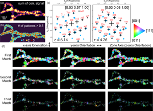
A common feature of polycrystalline samples is overlapping grains along the beam direction, leading to overlapping diffraction patterns. To demonstrate the ability of our method to work with overlapping grains, we have generated a combined set of diffraction patterns with three low index zone axes and random in-plane rotations, plotted in Figure 4a. Figures 4b–4d shows the first three matches returned by our ACOM code using a kernel size of  $\delta = 0.08$ Å, a zone axis step size of $1^{\circ }$, and a prefactor of $q_s \vert V_g\vert$. The multi-pattern peak deletion radius was slightly decreased from the default value of $0.04$ to $0.02$ Å to prevent removal of adjacent peaks as matches are assigned. Our ACOM code has correctly returned three zone axes which match the ground truth values. This example also demonstrates a procedure which could be used to map the location and orientation of multiple phases, even when the diffraction patterns overlap.

Fig. 4. ACOM of overlapping diffraction patterns. (a) Three overlapping diffraction patterns with randomly chosen in-plane rotations. (b) First match, (c) second match, and (d) third match returned by ACOM code. The fitted zone axes and correlation scores are inset into fits.
ACOM of Dynamical Simulated Diffraction Patterns
In diffraction experiments using thick specimens, strong dynamical diffraction effects such as multiple scattering can occur. This effect is especially pronounced in diffraction experiments along low index zone axes, where the diffracted peak intensities oscillate as a function of thickness. In order to test the effect of oscillating peak intensities on our ACOM method, we have simulated diffraction patterns for Cu, Ag, and Au fcc crystals, along multiple zone axes. Some example diffraction patterns for the  $[ 011]$ zone axis of Au are plotted in Figure 5a. We see that all diffraction spots have intensities which oscillate multiple times as a function of thickness.

Fig. 5. Dynamical simulated diffraction patterns. (a) Example diffraction patterns for Au oriented to the  $[ 011]$ zone axis for 10–80 nm thick slices. (b) Plots showing the mean zone axis misorientation in degrees as a function of thickness for Cu, Ag, and Au. Each plot shows the errors for correlation prefactors of $q_{{\rm s}} \vert V_{{\rm g}}\vert$ (red) and $q_{{\rm s}}$ (blue).
We performed ACOM by generating orientation plans with an angular sampling of  $2^{\circ }$, a correlation kernel size of 0.08 ${\ring{\rm A} }{}^{-1}$, and maximum scattering angles of $k_{{\rm max}} = 1.0$, 1.5, and 2.0 ${\ring{\rm A} }{}^{-1}$. We kept the radial prefactor of weighting set to $\gamma = 1$, and tested peak amplitude prefactors of $\omega = 1.0$, 0.5, and 0.0. The average zone axis angular misorientation as a function of thickness is plotted in Figure 5b. In total, we performed orientation matching on 3,750 diffraction patterns, and a total of 33,750 correlation matches on a workstation with an AMD Ryzen Threadripper 3960X CPU (2.2 GHz, baseclock). The typical number of patterns matched per second were of $\sim$80–90, 45–55, and 25–30 patterns/s for $k_{{\rm max}}$ values of 1.0, 1.5, and 2.0 ${\ring{\rm A} }{}^{-1}$, respectively.
As expected, the errors are higher than those achieved under kinematic conditions, and the trend for smaller errors with larger  $k_{{\rm max}}$ is also preserved (mean errors of 7.25 $^{\circ }$, 3.09 $^{\circ }$, and 1.39 $^{\circ }$ for $k_{{\rm max}}$ values 1.0, 1.5, and 2.0 ${\ring{\rm A} }{}^{-1}$, respectively, $\gamma = 1$, $\omega = 0.25$). We did not observe any dependence of the orientation accuracy on the simulation thickness. Despite the correlation prefactor $\vert Vg\vert$ performing well for the examples shown in Figure 1, for the dynamical diffraction simulations along zone axes it was out-performed by prefactors of both $\sqrt {\vert V_g\vert }$ ( $\omega = 0.5$) and omitting the peak amplitude prefactor altogether ( $\omega = 0$). We, therefore, suggest that when mapping samples with a large range of thicknesses, or many crystals aligned to low index zone axes, the position of the diffracted peaks is significantly more important than their amplitudes or intensities. One possible method to increase the average accuracy for a randomly orientated sample while using higher amplitude prefactors is to perform an experiment which recovers more kinematical values for the diffracted peak intensities, for example by precessing the electron beam when recording diffraction patterns (Midgley & Eggeman, Reference Midgley and Eggeman2015; Jeong et al., Reference Jeong, Cautaerts, Dehm and Liebscher2021). A precession experiment could however make the diffraction patterns of some grains more dynamical, and thus worsen the orientation accuracy for some probe positions. We note that there is likely no global optimal choice of orientation mapping hyperparameters for all materials and thicknesses, and this may be a worthwhile topic for future investigations.
4D-STEM ACOM of Twisted AuAgPd Nanowires
We have tested our ACOM algorithm with a 4D-STEM dataset collected for an AuAgPd nanowires. These nanowires are morphologically twisted into double helices via a colloidal growth process as previously reported by Wang et al. (Reference Wang, Wang, Sun, Zhang, Chen, Wang, Shen, Han, Lu and Chen2011). An image of the vacuum bullseye STEM probe is shown in Figure 6a. For each detector pixel, we have calculated the maximum value across all STEM probe positions to generate a maximum diffraction pattern, shown in Figure 6b. The beamstop used to block the center beam is visible, as well as various crystalline diffraction rings out to approximately 1.4  ${\ring{\rm A} }{}^{-1}$.

Fig. 6. 4D-STEM scan of twisted polycrystalline AuAgPd nanowires. (a) Diffraction image of probe over vacuum, showing the bullseye pattern. (b) Maximum of each pixel in diffraction space over all probe positions. (c) Histogram of all peak locations detected by correlation in py4DSTEM of (a) with each pattern included in (b). (d) HAADF-STEM image of the sample. (e) 1D histogram of scattering vectors, with fcc AuAg inverse plane spacings overlaid.
After performing the correlation peak finding algorithm in py4DSTEM, we have an estimated position and intensity of all detected Bragg peaks. A 2D histogram of these peaks, known as a Bragg vector map, is plotted in Figure 6c. Sharp polycrystalline diffraction rings are clearly visible, as well as false positives generated by the beamstop edge. These false positives were manually removed by using a mask generated from an image of the beamstop. A high-angle annular dark-field (HAADF) image was simultaneously recorded during the 4D-STEM data collection, which is shown in Figure 6d.
The final experimental pre-processing steps are to calibrate the diffraction pattern center, the elliptical distortions, and the absolute pixel size. We performed these steps by fitting an ellipse to the  $( 022)$ diffraction ring, and by assuming a lattice constant of $4.08 \, {\ring{\rm A} }$, corresponding to the fcc Au structure (Maeland & Flanagan, Reference Maeland and Flanagan1964). This process is explained in more detail by Savitzky et al. (Reference Savitzky, Zeltmann, Hughes, Brown, Zhao, Pelz, Pekin, Barnard, Donohue, DaCosta, Kennedy, Xie, Janish, Schneider, Herring, Gopal, Anapolsky, Dhall, Bustillo, Ercius, Scott, Ciston, Minor and Ophus2021). We assumed that the Ag lattice constant is similar to that of Au. Despite the presence of Pd in the nanowires, there was no significant presence of secondary grains corresponding to the smaller lattice of fcc Pd grains. An intensity histogram of the corrected Bragg peak scattering angles are shown in Figure 6e. We have overlaid the five smallest scattering angles of Au on Figure 6e to show the accuracy of the correction.
We have performed ACOM on the AuAgPd nanowire sample, with the results shown in Figure 7 shown for up to three matches for each diffraction pattern. For each probe position, the sum of the maximum detected correlation signals for up to three matches are shown in Figure 7a. The structure is in good agreement with Figure 6, though with additional modulations due to some grains generating more diffraction signal than others. Using a correlation intensity threshold of 0.5, we have plotted the number of matching patterns in Figure 7b. The threshold of 0.5 was arbitrary chosen as a lower bound for a potential match, as the correlation values are scaled by the experimental intensity. Examples of two matches to a single diffraction pattern are plotted in Figure 7c. In this figure, the correlation score for the first matched pattern was higher than the second. The second match found shows some deformation between the measured and simulated Bragg peak positions, and matches fewer peaks. It, therefore, produces a lower correlation score, which can be used to threshold the results as in Figure 7d. Note that the threshold values for inclusion of any given match into the orientation maps is always user-defined.

Fig. 7. Orientation mapping of polycrystalline AuAgPd nanowires. (a) Total of measured correlation signal for each probe position. (b) Estimated number of patterns indexed for each probe position. (c) Example of two orientations indexed from a single diffraction pattern, collected at the position indicated by the arrow shown in (b), with correlation scores inset. (d) Orientation maps of the three highest correlation signals for each probe position. A legend for the crystallographic orientation is shown above, and arrows indicate the direction of the  $x$- and $y$-axes, while the zone axis direction is out of the page.
Figure 7d shows the 3D orientations plotted as inverse pole figures for all probe positions, with the three best matches shown. Each image is masked by the total correlation signal, so that low correlation values are colored black. Almost every diffraction pattern with Bragg disks detected was indexed for at least one orientation with high confidence. Additionally, the patterns are very consistent, with a large number of adjacent probe positions recording the same orientation. Some secondary grains are also clearly visible in the second-best match, while very few patterns have been assigned a third match with high confidence.
In order to investigate the grain organization of the AuAgPd nanowires, we have performed clustering analysis on the orientation maps. Grains with similar orientations have been clustered together by looping through each probe position and comparing its orientation to its neighbors. Grains with at least 10 contiguous probe positions are shown in Figure 8a.  $( 111)$ planes which lie in the image plane are overlaid onto the grain strucure, colored by their orientation. Confirming our observations in Figure 7d, only a few grains with substantial overlap were reliably identified. This might be due to the low thickness of the sample (only a single grain along the beam direction), some grains not being oriented close enough to a zone axis to be detected, or multiple scattering deviations in the diffracted signal. There is a noticable bias in the orientation of the $( 111)$ planes, which tend to be oriented horizontally near the growth direction of the nanowires.

Fig. 8. Orientation analysis of grains in AuAgPd nanowires. (a) Crystal grains, with in-plane  $( 111)$ planes colored by orientation. (b) $( 111)$ planes shared by two overlapping grains.
One hypothesis for the growth mode of these twisted nanowires is that adjacent grains are connected by  $( 111)$ twin planes, forming local helical structures to give the observed twisted structures. To test this hypothesis, we determined the position of $( 111)$ planes from Figure 8a which are shared by two overlapping grains. Figure 8b shows the location of these shared $( 111)$ planes (with plane normal differences below $8^{\circ }$), colored by the normal vector of the plane. Many shared $( 111)$ planes were detected, most with normal vectors aligned to the wire growth direction. These observations support the hypothesis that these nanowires are composed of grains connected by $( 111)$ twin planes.
These experimental observations demonstrate the efficacy of our ACOM method. In order to improve these results, we will need to collect diffraction data with a wider angular range. This can be achieved by using precession electron diffraction (Rouviere et al., Reference Rouviere, Béché, Martin, Denneulin and Cooper2013), multibeam electron diffraction (Hong et al., Reference Hong, Zeltmann, Savitzky, DaCosta, Müller, Minor, Bustillo and Ophus2021), or by tilting the sample or beam and recording multiple 4D-STEM datasets (Meng & Zuo, Reference Meng and Zuo2016).
Conclusion
We have introduced an efficient and accurate method to perform automated crystal orientation mapping, using a sparse correlation matching procedure. We have implemented our methods into the open source py4DSTEM toolkit, and demonstrated the accuracy of our method using simulated diffraction patterns, where we show that lowering or removing the peak-intensity weighting can improve the accuracy for thick samples with substantial dynamical diffraction. We also applied ACOM to an experimental scan of a complex helical polycrystalline nanowire, where we were able to identify shared twin planes between adjacent grains which may be responsible for the twisted helical geometry. All of our methods have been made freely available to the microscopy community as open source codes. We believe that our implementation of ACOM is efficient and accurate enough to be incorporated into automated online TEM software (Spurgeon et al., Reference Spurgeon, Ophus, Jones, Petford-Long, Kalinin, Olszta, Dunin-Borkowski, Salmon, Hattar, Yang, Sharma, Du, Chiaramonti, Zheng, Buck, Kovarik, Penn, Li, Zhang, Murayama and Taheri2021). In the future, we will improve our ACOM method using machine learning methods (Munshi et al., Reference Munshi, Rakowski, Savitzky, Zeltmann, Ciston, Henderson, Cholia, Minor, Chan and Ophus2021), and we will extend our ACOM methods to include multibeam electron diffraction experiments (Hong et al., Reference Hong, Zeltmann, Savitzky, DaCosta, Müller, Minor, Bustillo and Ophus2021).
Source Code and Data Availability
All code used in this manuscript is available on the py4DSTEM GitHub repository, and the tutorial notebooks are available on the py4DSTEM tutorial repository. The experimental dataset used in this paper is available as https://drive.google.com/drive/folders/1_fXBc2DO4qOeXyA3idml-ehaqf1y8Mke?usp=sharing, and the simulated datasets are available at https://drive.google.com/drive/folders/1oZ3Q2rTMqoqtvzNlzdeyIbYHaV6wUz11?usp=sharing.
Acknowledgments
We thank Karen Bustillo for helpful discussions. C.O. acknowledges support of a U.S. Department of Energy Early Career Research Award. S.E.Z. was supported by the National Science Foundation under STROBE Grant no. DMR 1548924. A.B., B.H.S., and py4DSTEM development are supported by the Toyota Research Institute. A.R. is supported by the 4D Data Distillery project, funded by the U.S. Department of Energy. Work at the Molecular Foundry was supported by the Office of Science, Office of Basic Energy Sciences, of the U.S. Department of Energy under Contract No. DE-AC02-05CH11231. This research used resources of the National Energy Research Scientific Computing Center (NERSC), a U.S. Department of Energy Office of Science User Facility located at Lawrence Berkeley National Laboratory, operated under Contract No. DE-AC02-05CH11231.


 Open access