

Graphene and carbon nanotubes (CNTs) are promising materials for many applications due to their chemical, mechanical, and electrical properties. There is an emerging research area that is focused on combining CNTs and graphene for applications such as sensors, solar cells, supercapacitors, and optoelectronic devices. This is achieved by growing a three-dimensional (3D) network of CNTs on graphene or ultrathin graphite layers (CNTs/G). The great potential of the 3D CNTs/G composite structure in such devices is due to its efficient charge transfer and carrier collection superior to 2D ultrathin graphite sheets alone.
In practice, the growth of 3D CNTs/G is challenging for two reasons: first, graphene and CNTs have different growth conditions, and second, controlling the density and length of CNTs is challenging. Current growth techniques necessitate complicated multistep processes that limit the applicability of CNTs/G hybrid structures in devices. A research team at KU Leuven led by Jin Won Seo has simplified the growth techniques into a one-step process where CNTs and ultrathin graphite layers are grown simultaneously.
The technique utilizes copper (Cu) nanoparticles, formed by first oxidizing a Cu foil at 190°C for 10 min, which causes the surface to roughen, then annealing under hydrogen flow, thereby reducing the oxide layer and generating a Cu surface roughened by Cu nanoparticles. Ultrathin graphite layers grow from absorbed carbon atoms on the flat surface of Cu foil after introducing CO2 and acetylene into the chamber, while CNTs form from C atoms concentrated at the nanoparticles. Both the graphite layer and CNTs thus grow simultaneously in one step rather than the conventional multistep process.
“Although the ideal growth conditions for graphene and CNTs are totally different, their growth is competitive. Therefore, as soon as the 2D growth is established, it is difficult to initiate CNT growth. However, the Cu nanoparticles formed by the oxidation/reduction are able to locally promote CNT growth and to form 3D CNTs/G,” says Lee-Woon Jang of KU Leuven, the first author of the research recently reported in Scientific Reports (doi:10.1038/s41598-019-48725-w).
The research team characterized the structural quality of the 3D CNTs/G hybrid by using Raman spectroscopy and transmission electron microscopy (TEM). TEM showed that CNTs had a diameter of ∼25 nm, while graphite layers were ∼10 nm thick corresponding to ∼20 layers of graphene. Conductive atomic force microscopy (AFM) embedded inside a scanning electron microscope was used to study the electrical properties. A network of CNTs/G produced 0.71 mA at 2 V compared to 0.62 mA for bare ultrathin graphite proving that the CNTs/G hybrid has better conductivity, due to increased contact area with the AFM. “Comparing the electrical properties of bare ultrathin graphite, a single and multiple CNTs/G network was the ultimate proof of better conductivity,” Seo says.
As proof of concept, the researchers fabricated perovskite optoelectronic devices using the hybrid 3D CNTs/G and a bare ultrathin graphite layer to compare their electrical properties. Time-resolved photoluminescence measurements showed that the lifetime of carriers in the 3D CNTs/G structure is 41% shorter than that in bare ultrathin graphite (10 ns and 17 ns) due to additional carrier transport by CNTs, and a high nonradiative recombination rate of photogenerated holes and electrons by defects. Both high carrier recombination and easier carrier collection are key to the better performance of the 3D CNT/G-based devices for applications, such as in solar cells, detectors, batteries, piezoelectric generators, and membranes.
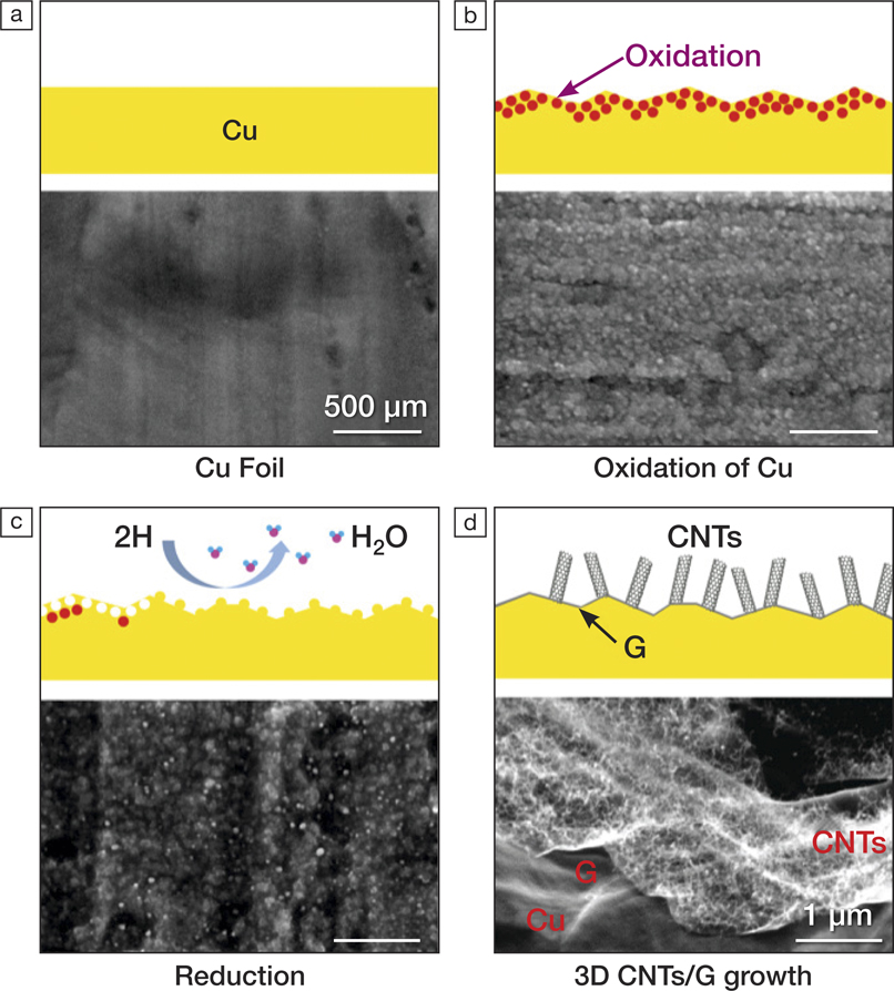
Schematic drawing illustrating the growth procedure of the three-dimensional carbon nanotubes/graphene (3D CNTs/G) networks and respective scanning electron microscope images demonstrating the change of the Cu surface after each step. (a) Pristine Cu foil, (b) oxidized Cu surface after annealing on a hot plate, (c) surface after the reduction step in H2-rich atmosphere, and (d) grown 3D CNTs/G network. Credit: Scientific Reports.
László Forró, a professor at École Polytechnique Fédérale de Lausanne, Switzerland, and an expert in the physics of nanomaterials and novel electronic materials, says, “3D CNTs/G hybrid structures allow extending the excellent electrical conductivity of graphene and CNTs to three dimensions. The KU Leuven team has succeeded to develop a simple and efficient one-step growth procedure for 3D CNTs/G hybrid, which gives opportunities to significantly improve the performance of various devices through efficient carrier collection.”
