


Introduction
The demand for solar energy continues to climb with over 50 GW/year of photovoltaics installed globally in recent years [Reference Kato1, Reference Philipps and Warmuth2]. The majority of solar cells are produced from crystalline silicon, but thin film materials such as CuInSe2 (CIS) and alloys of Cu(In,Ga)Se2 (CIGS) have also been shown to be good light absorbers for thin film photovoltaic devices with conversion efficiencies above 14% in commercial modules [Reference Kato1–Reference Siebentritt3].
Polycrystalline CIGS thin films have grain size on the order of 0.3–2.0 µm depending on deposition and process conditions [Reference Caballero4–Reference Abou-Ras8]. When the average grain size is smaller than the thickness of the CIGS film, the generated current will pass through multiple grain boundaries, which are potential recombination centers for the charge carriers [Reference Siebentritt3–Reference Nichterwitz5]. For many semiconductors materials such as Si or GaAs, the presence of grain boundaries will degrade the solar cell performance; however, polycrystalline Cu(In,Ga)Se2 solar cells can reach good conversion efficiencies despite the presence of a high grain boundary density [Reference Nichterwitz5, Reference Abou-Ras8]. Rau et al. modeled the influence of GBs on CIGS solar cell efficiencies and predicted a decrease in efficiency when the defect density at the grain boundary exceeded ~ 1011 cm-2 [Reference Rau9]. This trend appeared over a wide range of defect energies, and their results predict a significant decrease in efficiency for CIGS films with a small grain size [Reference Rau9]. This article describes some experiments to better understand the effect of grain boundaries on CIGS thin film photovoltaic performance.
Materials and Methods
Specimen preparation
Conventional scanning electron microscopy (SEM) images of thin film surfaces were recorded using a FEI Helios NanoLab G3 dual-beam focused-ion-beam SEM. Prior to the SEM analysis, the CIGS cells were etched in dilute (10% vol.%) HCl solution for several minutes to remove the top contact layers, which consisted of a transparent conductive oxide and CdS film. The CIGS thin films were fabricated at NuvoSun using a two-stage process in which a Cu-Ga-In alloy precursor was first partially selenized and then fully selenized at ~ 550–600oC in a separate reactor roll-to-roll line. A focused-ion beam of 9.3 nA was used to ion-polish the sample surface at a glancing angle prior to electron backscatter diffraction (EBSD) experiments. The milled region was about 50 µm wide, which provided a relatively large area for EBSD. Atomic force microscopy (AFM) showed that ion milling removed about 100–200 nm of material.
Electron backscatter diffraction
EBSD has been used extensively to determine grain properties such as texture and recrystallization, as well as failure analysis and strain mapping, but only to a limited extent for CIGS thin films [Reference Wright and Nowell10–Reference Brewer and Michael12]. In this study, EBSD patterns were collected for different thin film samples in order to determine the grain size distribution and orientation [Reference Wright and Nowell10–Reference Brewer and Michael12]. A typical instrument configuration is shown in Figure 1a, which shows a Helios FIB-SEM and EDAX EBSD detector. Figure 1b shows the orientation of the sample with respect to the EBSD detector.
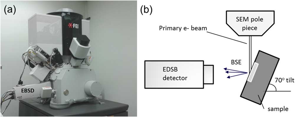
Figure 1 Instrumentation. (a) Helios G3 FIB-SEM with an EDAX EBSD detector. (b) Schematic of the EBSD setup showing sample orientation relative to the EBSD camera. The sample is tilted at an angle of 70o toward the detector.
The EBSD data were collected using an EDAX detector with OIM-Team software at 20 keV, 13 nA electron current, 8 mm working distance, and a magnification of 10 k×. Experimental EBSD conditions were as follows: map size area = 12 μm × 12 μm; pixel size (medium) = 0.04 μm, the bin size = 5 × 5 ; gain = 300, exposure time = 3.66 msec, frame averaging = 5, frames per second = 270 fps ( ~55 patterns per sec with frame averaging of 5×).
The EBSD signal originates from approximately the top ~20 nm of the sample, and therefore the quality of EBSD data is sensitive to crystal perfection near the surface [Reference Wright and Nowell10–Reference Maitland and Sitzman13]. The CIGS structure is tetragonal, with a c/a of ~2.0, but the structure was indexed assuming a pseudo cubic symmetry to improve the indexing [Reference Maitland and Sitzman13]. The orientation of each pixel is calculated during pattern collection and assigned a confidence index based on the quality of the pattern. After the entire data set of EBSD patterns is collected, each pixel is assigned to a specific grain. For pixels that had a low confidence index, a standard clean-up procedure was applied to assign pixels to grains. The clean-up procedure consisted of single “grain dilation” for each data set using the following criteria: (1) a grain must contain multiple rows of pixels, (2) single dilation iteration, (3) pixel size of 0.04 µm (40 nm), (4) minimum grain size of five pixels, and (5) an inter-grain tolerance angle of 5 degrees. Grains smaller than 0.1 µm were not included in grain-size analysis. Similar EBSD work by Abou-Ras et al. used an Ar ion milling procedure to prepare cross-sectional CIGS samples to minimize the beam damage. The pixel size used for their investigation was 10–50 nm, and the authors excluded grains with diameters ≤ 0.2 µm [Reference Abou-Ras8].
Atomic force microscopy
Samples of etched and ion-polished CIGS were imaged using peak force (PF) tapping AFM techniques. The AMF images were obtained on a Bruker Icon using a Nanoscope V controller (software v.8.15). Cantilevers employed were Bruker Scanasyst (air) with the following settings: PF set point = 1.2 V; noise threshold = 0.5 nm; PF amplitude = 300 nm; Z range = 12 μm; PF engagement set point = 0.15 V. Scan sizes were 50 µm × 50 µm. All images were captured at 1024 lines of resolution. All images were produced using SPIP v.6.3.5 software (Scanning Probe Image Processor, Image Metrology, Denmark). A 2nd order average plane fit with a zero-order LMS and mean set to zero plane fit was used to flatten the images. All postprocessing measurements were done using SPIP software as well.
Results
CIGS cells : process and device properties
The grain properties (size, texture, and relative orientation) were investigated using EBSD of cells that were grown under different reactor conditions but which had a similar level of performance (Table 1). Device efficiencies ranged from 10–11% efficiency, and the open circuit voltage (Voc) ranged from 590 mV to 629 mV.
Table 1 NuvoSun cell performance. Device efficiency (in %) and open circuit voltage (Voc in volts) for each device. The solar cell efficiency refers to the efficiency of converting light into electricity. Open-circuit voltage, the maximum voltage available from a solar cell, is also a measure of performance. Commercial devices with polycrystalline silicon have open-circuit voltages on the order of ~ 600 mV, whereas organic solar devices can have open-circuit voltages in excess of 600 mV.

Surface roughness of as-received NuvoSun CIGS
AFM was used to investigate the morphology and roughness of the as-received CIGS surfaces for the various devices. Figures 2a-2c show AFM images of the surfaces that indicated the grain structure for Device 1 was more faceted compared to Devices 2 and 3. The average surface roughness of the CIGS films, as measured by AFM techniques, varied from 60 nm to 94 nm. Figure 3 shows SEM images of CIGS film surfaces. The SEM images also revealed variations in surface structure and roughness among the samples, and all of the as-received samples contained sub-micron porosity, typically located at grain boundary junctions.
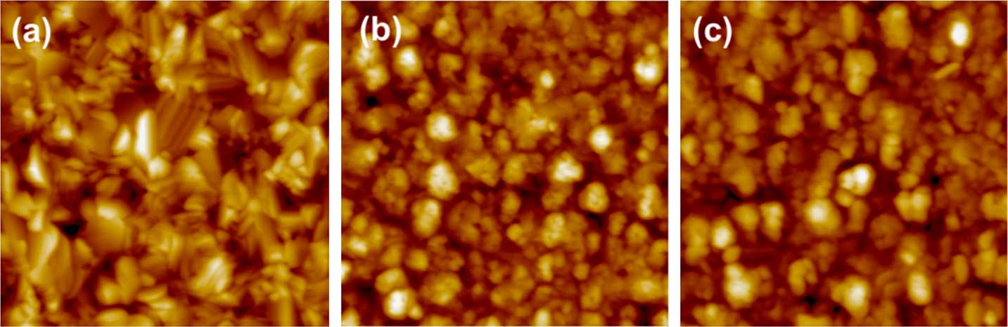
Figure 2 AFM images for Devices 1 to 3 in images (a) to (c). Fields of view are 10 µm × 10 µm. The average surface roughness (Ra) values for the cells were determined from 50 µm × 50 µm regions. The Ra values by AFM for Devices 1–3 were 60.1 nm, 73.8 nm, and 94.7 nm, respectively.

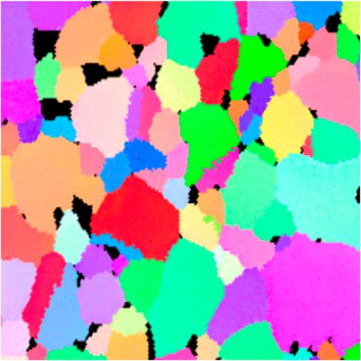
Figure 3 SEM plan view images and EBSD inverse pole figures (IPFs) of the CIGS surface for the three devices. (a–c) SEM surfaces images of Devices 1–3. (d–f) Corresponding inverse pole figures from etched CIGS surfaces (IPF raw data) for Devices 1–3. The red, green, and blue refer to grains with <001>, <102>, and <112> orientations. The average AFM surface roughness (Ra) values for the cells were 60.1 nm, 73.8 nm, 94.7 nm, respectively. Note that the SEM images and IPF maps were not from the same areas. No cleaning steps were applied to these IPF maps. Image width = 7.5 µm.
EBSD of NuvoSun cells
Grain orientation maps, derived from the EBSD patterns, are usually displayed in inverse pole figure (IPF) coloring for easy visualization of the different orientations. Figures 3d to 3f show the IPFs for the three different as-received CIGS. Inverse pole figures here use a coloring scheme for the orientation of each grain similar to that for cubic grains (Figure 4). The color of each grain is used as a description of crystal orientation, and an abrupt orientation change (change in color) defines a grain or phase boundary.

Figure 4 (a) Quadrant of stereogram and (b) standard triangle showing the coloring scheme used in IPFs for tetragonal symmetry with c/a ratio = 2.0.
For most samples, it was not possible to collect EBSD data from all locations because of the sample roughness as shown in Figures 3d to 3f. A significant portion of the IPF maps appear “black” in color, indicating a low confidence index (< 0.1), which means that the patterns collected from these regions could not be indexed with a high level of certainty. The reason for this is often poor pattern quality, but in this case the reason was attributed to the high surface roughness which blocks some of the scattered electrons from reaching the detector. Note that Device 1 was relatively smooth (Ra = 60 nm) compared to the other films, and most of the grains could be indexed. Devices 2 and 3 had higher average surface roughness values (Ra = 74 nm and 94 nm), and many areas could not be indexed.
Surface preparation of devices
Mechanical polishing methods using colloidal silica techniques were first attempted to reduce the surface roughness of the samples, but this resulted in poor EBSD pattern quality due to mechanical damage near the surface. Thus, focused ion-beam milling was used to reduce the sample roughness. In this technique, the samples were ion-milled at a glancing angle to the surface. Figure 5 shows SEM images of a CIGS surface before and after ion milling.
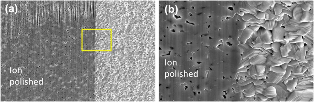
Figure 5 Ion-beam polishing. (a) Secondary electron SEM (plan view) image of the CIGS surface before (right side) and after (left side) the ion-milling polishing procedure for Device 1. Image width = 52 µm. Image (b) is five times the magnification of image (a). Image width = 10.4 µm. Samples are oriented so that the stainless steel rolling direction is aligned with the long direction of the page. Some enlargement of the pores may occur as an artifact during the ion-milling process.
The goal of the ion-milling step was to remove a minimum amount of material (~100 nm) that would improve the EBSD pattern quality and still allow information on the grain size and orientation to be obtained near the original surface. This depth represents ~ 10% of the total CIGS films thickness (~ 1.2 µm). Ion-milling was done at a glancing angle for several minutes over a width of 50 µm to provide a sufficient area for EBSD analysis. AFM measurements indicated that the surface roughness decreased substantially after ion-milling; however, typically ~200–250 nm was removed from the surface by ion-milling in order to provide a smooth surface. The depth of the CIGS removed during the ion-milling step was estimated by using AFM measurements of the median height difference between the ion-polished and as-received regions as shown in Figure 6.
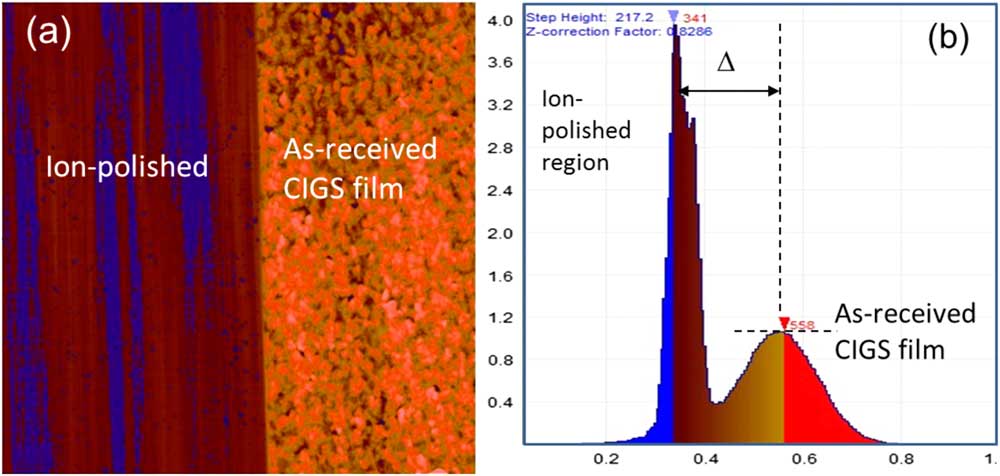
Figure 6 (a) AFM scan of 50 µm × 50 µm region across both as-deposited CIGS and ion-polished regions. (b) Histogram showing the height distribution for scanned area (x-axis in µm). The as-deposited film shows a broad distribution of heights (over an area of ~ 25 µm × 50 µm) due to a combination of the thin film roughness plus a non-uniform stainless steel substrate. Conversely, the ion-polished area shows a relatively narrow height distribution. The depth removed during the ion-milling step was estimated by comparing the median height of the two regions. The difference in median heights for this area was ~ 234 nm.
Figure 7 shows inverse pole figures after ion-polishing for Devices 1–3. In general, we observed that the quality (confidence index) of the EBSD patterns collected from ion-polished surfaces was lower compared to as-received surfaces. This was attributed to surface damage from Ga ion-implantation during ion-milling; however, the quality of EBSD patterns collected from ion-milled surfaces was sufficient for indexing of the grains without additional surface treatment (for exmaple etching or Ar ion milling to remove surface damage). It is interesting to note that while porosity was observed in all devices (based on both SEM imaging and EBSD data), it does not appear to degrade device performance dramatically at this efficiency level since all devices had 10–11% efficiency. Regions with a low confidence index (pores) are denoted in black. The EBSD patterns were collected over regions 12 μm × 12 μm in size for each sample in order to collect a sufficient number of grains for statistical analysis, but a smaller region (7 μm × 7 μm) is shown in Figure 7 for clarity.
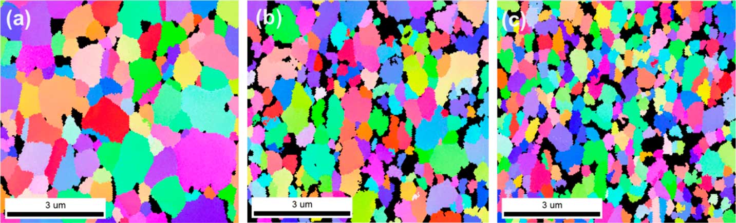
Figure 7 Inverse pole figure EBSD data (a) to (c) show grain size and orientation for Devices 1, 2, and 3, respectively. A single dilation clean-up step was used as described in the text. Samples were oriented so that the stainless steel rolling direction is aligned with the long direction of the page. Regions with a Confidence Index < 0.1 are shown in black.
Grain size measurements
The EBSD data were used to determine the grain size distribution for Devices 1–3 (Figure 8). The average grain size for Device 1 was ~ 0.6 µm, which was significantly larger than the average size ~ 0.4 µm for Devices 2 and 3. The CIGS grain size diameter can be reasonably represented by a log-normal distribution as shown in Figure 8.
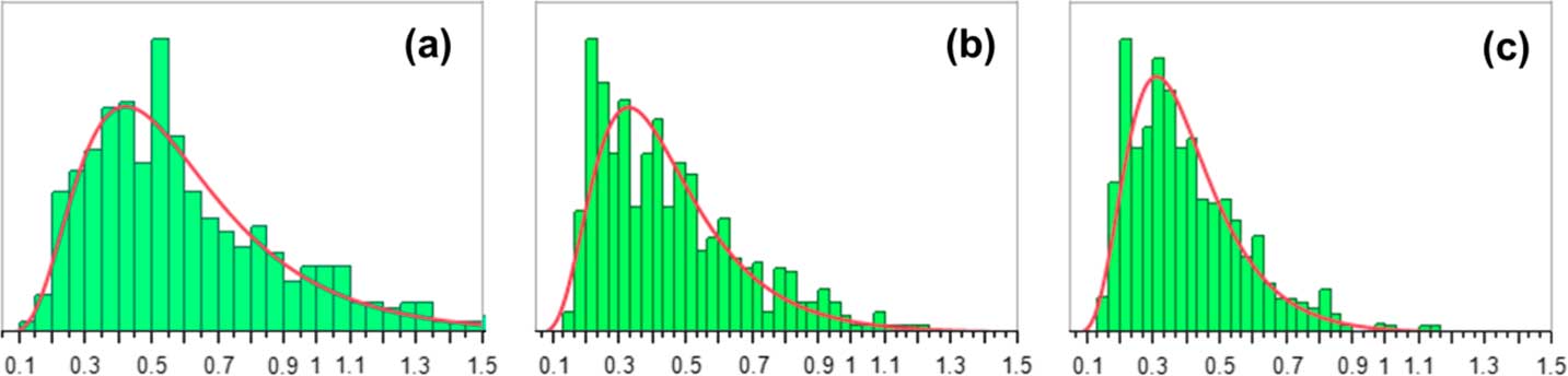
Figure 8 Grain sizes in µm and log normal fits for Devices 1–3 in (a) to (c), respectively. Device 1 had an average grain size of 0.6 µm, whereas the average grain size for the other two devices was 0.4 µm.
The performance levels of Devices 1–3 were all similar, and therefore the average grain size did not correlate with device performance at this efficiency level of 10–11%. This result is consistent with previous work, which showed that the grain size has a limited impact on device performance, and other factors such as recombination at the heterojunction interface, internal potential fields, or recombination at the back contact may play more significant roles [Reference Siebentritt3, Reference Abou-Ras8]. In addition, the role of the relative grain orientation or porosity may also be a limiting factor to attainment of higher efficiencies. It is interesting to note that Device 2 was annealed for additional time (40 minutes) at 600oC in an Se reactor to promote grain growth compared to Device 1, but this anneal did not have a significant effect on grain growth.
Grain boundary type
The distribution of low- and high-angle grain boundaries was also investigated. Low-angle grain boundaries are defined as adjacent grains with only 2 o–15 o misorientation. The misorientation angle between grains is shown in Figures 9a and 9b for Devices 1 and 3. Most grain boundaries were high-angle (shown in blue), and special high-symmetry grain boundaries of 60o are denoted by green color. An alternate way of presenting the data is to show the distribution of misorientation angles between adjacent grains as shown in Figures 9c and 9d, which indicated that few low-angle grain boundaries were present (red lines).
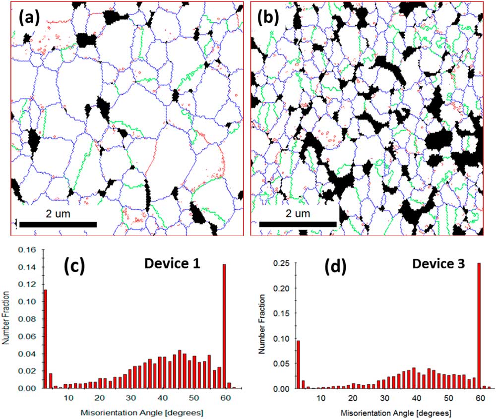
Figure 9 Misorientation angles for grains in Devices 1 and 3 shown in (a) and (b). The “Red” lines show the low-angle grain boundaries, whereas high-angle grain boundaries are denoted by the blue lines. Special high-symmetry grain boundaries of 60o are shown in green. Bar graphs in (c) and (d) show the distribution of the misorientation angles between all grains in each device. Voids are excluded in the grain boundary analysis.
The misorientation angles shown in Figures 9c and 9d exhibit a broad distribution centered on 40o–45o, which is consistent with a random orientation [11]. This result agrees with X-ray diffraction measurements conducted on similar devices grown using a two-step selenization process. Conversely, thin films of CIGS grown by co-evaporation often display <220/204> and <112> grain textures [Reference Contreras7].
Discussion
There are several proposed models used to explain the properties of grain boundaries in CIGSe [Reference Siebentritt3, Reference Contreras7, Reference Baier15]. In the electronic barrier model, trapped charge at the grain boundary causes local bending of the conduction and valence bands adjacent to the grain boundary. In this model, a downward band bending toward GBs would favor recombination of carriers, while an upward band bending would repel minority carriers and reduce recombination [Reference Baier15, Reference Hanna16].
Baier et al. investigated the symmetry of GBs that influences GBs electronic properties [Reference Baier15]. Their results showed that special (Σ = 3) grain boundaries typically were neutral (zero potential), while the non- Σ = 3 grain boundaries had a wider range in potential from positive to negative. Hannah et al. also investigated CIGS samples, and their results indicated that samples with a random texture had a more negative contact potential near the grain boundaries compared to the samples with a strong (220/204) texture [Reference Hanna16]. These studies suggest the grain boundary orientation and grain boundary defects may limit device performance as predicted by Rau et al. [Reference Rau9].
Kelvin probe force microscopy (KPFM) is one method that has been used to obtain spatially resolved information of the work function at the grain boundary and at adjacent grains [Reference Baier15, Reference Hanna16]. Similar experiments are currently in progress to characterize the surface potential of CIGS devices near the heterojunction interfaces and grain boundaries using KPFM and EBSD in order to better understand the correlation between grain boundary misorientation and device efficiency.
Conclusion
Collection of high-quality EBSD grain size and grain orientation data from as-received CIGS devices was limited due to the surface roughness, and many grains could not be properly indexed. This issue was circumvented by ion-polishing the CIGS samples at a glancing angle to reduce surface roughness. The quality of EBSD patterns after ion-polishing was adequate for indexing, although the patterns were then collected at a depth of ~200–250 nm from the original surface.
The CIGS grain size did not have a significant impact on device performance (at this level of efficiency), and other factors are expected to play a dominant role. The EBSD results indicated that the majority of grain boundaries in these devices were high-angle boundaries. The EBSD results also showed that the CIGS films did not have a strong texture, which agrees with previous X-ray diffraction measurements for devices grown using a two-step selenization process. Typically, CIGS thin films grown by co-evaporation will often display a <220/204> and <112> grain texture.
The SEM and EBSD data indicated that there was a significant variation in the porosity among the different devices, but this did not lead to differences in device performance. The extent to which the high-angle grain boundaries and porosity will limit device performance at higher efficiency levels is under investigation.
Acknowledgements
The authors wish to thank S. I. Wright and M.M. Nowell of EDAX for their guidance in the EDSB analysis.


