


Introduction
Wide band-gap semiconductors, such as AlxGa1–xN and GaN, are used in a wide range of technologically important optical and electrical devices, including high brightness LEDs, high electron mobility transistors (HEMTs) and laser diodes (Roccaforte et al., Reference Roccaforte, Fiorenza, Greco, Lo Nigro, Giannazzo, Iucolano and Saggio2018; Tsao et al., Reference Tsao, Chowdhury, Hollis, Jena, Johnson, Jones, Kaplar, Rajan, Van de Walle, Bellotti, Chua, Collazo, Coltrin, Cooper, Evans, Graham, Grotjohn, Heller, Higashiwaki, Islam, Juodawlkis, Khan, Koehler, Leach, Mishra, Nemanich, Pilawa-Podgurski, Shealy, Sitar, Tadjer, Witulski, Wraback and Simmons2018). Controlled doping of these alloys is crucial for control of the electronic properties of the epitaxial layers and hence optimal device performance. Si and Mg are typically employed as the n- and p-type dopants, respectively, in both AlxGa1–xN and GaN (Van de Walle et al., Reference Van de Walle, Stampfl, Neugebauer, McCluskey and Johnson1999).
Optoelectronic devices operating in the ultraviolet (UV) spectral range and those used for high power, high frequency electronic devices require wider band-gap materials, and AlxGa1–xN with increasing AlN content (x ≥ 0.5) is often the material of choice (Amano et al., Reference Amano, Collazo, Santi, Einfeldt, Funato, Glaab, Hagedorn, Hirano, Hirayama, Ishii, Kashima, Kawakami, Kirste, Kneissl, Martin, Mehnke, Meneghini, Ougazzaden, Parbrook, Rajan, Reddy, Römer, Ruschel, Sarkar, Scholz, Schowalter, Shields, Sitar, Sulmoni, Wang, Wernicke, Weyers, Witzigmann, Wu, Wunderer and Zhang2020). It is challenging to effectively dope AlxGa1–xN, with Si and Mg at such high AlN contents because as the bandgap increases the ionization energies also increase. At the same time, a very high Si doping concentration is needed to achieve low resistivity AlxGa1–xN layers (Mehnke et al., Reference Mehnke, Trinh, Pingel, Wernicke, Janzén, Son and Kneissl2016; Foronda et al., Reference Foronda, Hunter, Pietsch, Sulmoni, Muhin, Graupeter, Susilo, Schilling, Enslin, Irmscher, Martin, Wernicke and Kneissl2020).
The procedure of quantitative measurement of Si concentration in semiconductor layers will enable the optimization of growth conditions in order to achieve high efficiency devices. In this paper, wavelength-dispersive X-ray (WDX) spectroscopy within an electron probe microanalyser (EPMA) was employed to measure donor levels. The WDX technique is routinely used for the quantification of major elements (concentration > 1,000 ppm) and minor elements (100–1,000 ppm), and during the last decade, it has been successfully used for trace-element analyses (below 100 ppm and down to 10 ppm) (Donovan et al., Reference Donovan, Lowers and Rusk2011). WDX analysis has several advantages over other analytical methods such as dynamic secondary ion mass spectrometry (D-SIMS), energy-dispersive X-ray spectroscopy (EDX), laser ablation inductively coupled plasma mass spectrometry (LA-ICP-MS), and micro particle-induced X-ray emission (μ-PIXE). These include high lateral spatial resolution (sub-μm), its nondestructive nature and that it does not usually require extensive standards due to the existence of well-developed matrix correction procedures. In addition, the EPMA allows acquisition of other analytical signals simultaneously with the high-resolution composition mapping, such as cathodoluminescence (CL; Martin et al., Reference Martin, Edwards, O'Donnell, Dawson, Jeon, Liu, Rice and Watson2004; Lee et al., Reference Lee, Martin, Trager-Cowan and Edwards2005; Edwards & Martin, Reference Edwards and Martin2011; Edwards et al., Reference Edwards, Jagadamma, Bruckbauer, Liu, Shields, Allsopp, Wang and Martin2012), electron beam-induced current (EBIC; Wallace et al., Reference Wallace, Edwards, Kappers, Hopkins, Oehler, Sivaraya, Allsopp, Oliver, Humphreys and Martin2014), and electron channeling contrast imaging (ECCI) signals (Naresh-Kumar et al., Reference Naresh-Kumar, Alasmari, Kusch, Edwards, Martin, Mingard and Trager-Cowan2020). Some limitations of the WDX technique are that depth resolution is a function of the electron accelerating voltage, which must be high enough to excite all the relevant X-ray lines, preferably with an overvoltage ratio of at least 2 to ensure accurate analysis, particularly when approaching detection limits. These limitations also introduce constraints on the minimum sample thickness (Newbury, Reference Newbury2002) and depth profiling, where SIMS performs strongly including for nitride semiconductor structures (Martin et al., Reference Martin, Rading, Kersting, Tallarek, Nogales, Amabile, Wang, Katchkanov, Trager-Cowan, O'Donnell, Watson, Matias, Vantomme, Lorenz and Alves2006; Wei et al., Reference Wei, Zhao, Wang, Zeng and Li2014; Michałowski et al., Reference Michałowski, Złotnik and Rudziński2019; Pickrell et al., Reference Pickrell, Armstrong, Allerman, Crawford, Cross, Glaser and Abate2019). Two of these works employed time-of-flight SIMS (TOF-SIMS) which has a number of advantages over D-SIMS, including dual-source depth profiling where the two ion beams have been optimized for their respective tasks, although work is needed to achieve the same detection limit for dopants (Klump et al., Reference Klump, Zhou, Stevie, Collazo and Sitar2018).
The capability of the WDX technique for measuring dopants within semiconductor epilayers has been reported by Deatcher et al. (Reference Deatcher, Bejtka, Martin, Romani, Kheyrandish, Smith, Rushworth, Liu, Cheong and Watson2006) and Kusch et al. (Reference Kusch, Mehnke, Enslin, Edwards, Wernicke, Kneissl and Martin2017). The latter compared WDX data for Si concentration ranges 40–350 ppm (3 × 10¹⁸–2.8 × 1019 cm−3) in AlxGa1–xN with commercially performed D-SIMS on some of the samples in the study. Both measurement methods showed the same general trend: a linear increase in the Si concentration with increasing SiH4/III (silane to group-III ratio), but the Si concentration measured by WDX was higher by a factor of approximately 2 compared with D-SIMS. The reason for the discrepancy between the different types of measurement was not clarified at the time (Kusch et al., Reference Kusch, Mehnke, Enslin, Edwards, Wernicke, Kneissl and Martin2017). However, the reports in Deatcher et al. (Reference Deatcher, Bejtka, Martin, Romani, Kheyrandish, Smith, Rushworth, Liu, Cheong and Watson2006) and Robin et al. (Reference Robin, Mollard, Guilloy, Pauc, Gentile, Fang, Daudin, Amichi, Jouneau, Bougerol, Delalande and Bavencove2016) show that it is possible to use X-ray microanalysis to measure doping levels in semiconductor epilayers, with Robin et al. using EDX to address quantitation of dopants. The report of Deatcher et al. (Reference Deatcher, Bejtka, Martin, Romani, Kheyrandish, Smith, Rushworth, Liu, Cheong and Watson2006) shows that Mg measurement in GaN gives very good agreement between WDX and D-SIMS. The question of why WDX measurement appears to over-estimate values for the Si doping is the subject of this investigation. Donovan et al. (Reference Donovan, Lowers and Rusk2011) developed optimum measurement practices for WDX trace analysis which we will apply in the analysis of Si doping.
Over the years, many research groups have addressed the trace-element capabilities of the WDX technique. Some early examples include the analysis of Ge distribution in iron meteorites (Goldstein, Reference Goldstein1967), transition elements in ferromagnesian silicate minerals (Merlet & Bodinier, Reference Merlet and Bodinier1990), trace elements in minerals (McKay & Seymour, Reference McKay and Seymour1982), and trace elements in glass (Fialin et al., Reference Fialin, Remy, Richard and Wagner1999). More recent works focus on specific situations or on refinements of the technique and conditions for trace analysis, such as the works from Allaz et al. (Reference Allaz, Razvan-Gabriel, Reusser and Martin2019), Batanova et al. (Reference Batanova, Sobolev and Magnin2018), Buse et al. (Reference Buse, Wade, Llovet, Kearns and Donovan2018), Carpenter et al. (Reference Carpenter, Counce, Kluk and Nabelek2002), Donovan et al. (Reference Donovan, Lowers and Rusk2011, Reference Donovan, Singer and Armstrong2016), Fournelle (Reference Fournelle2007), von der Handt et al. (Reference von der Handt, Allaz and Neill2016), Jercinovic et al. (Reference Jercinovic and Williams2005, Reference Jercinovic, Williams, Allaz and Donovan2012), Reed (Reference Reed2000, Reference Reed2002), Sato et al. (Reference Sato, Mori, Takakura and Notoya2007), and Zhang et al. (Reference Zhang, Koepke, Wang, Wolff, Wilke, Stechern, Almeev and Holtz2016).
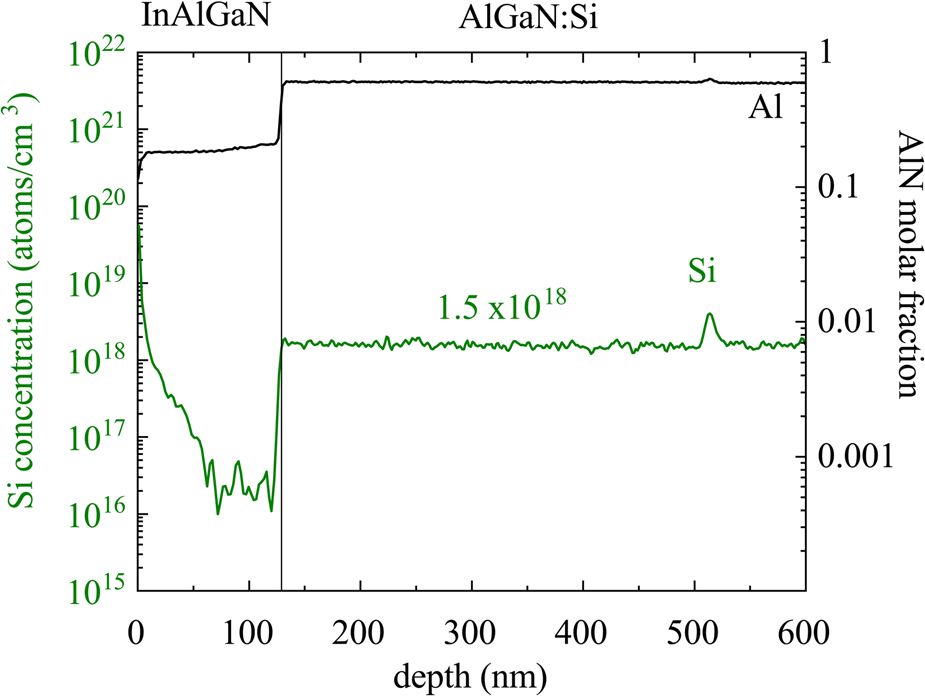
In this paper, we will consider how to measure Si, at dopant levels, in semiconductor epilayers such as GaN and AlxGa1–xN where inherent contamination of the sample surfaces with additional Si is suspected to be the cause of a discrepancy between the results from D-SIMS and WDX. Si incorporation is known to be a contaminant during the metal-organic chemical vapor deposition (MOCVD) growth of GaN and AlxGa1–xN (Koleske et al., Reference Koleske, Wickenden, Henry and Twigg2002; Pickrell et al., Reference Pickrell, Armstrong, Allerman, Crawford, Cross, Glaser and Abate2019). Typical growth temperatures are in the region of 1,100°C, in order to promote the breakup of the ammonia molecules and adatom mobility on the growing surface, and it should be noted that the graphite susceptors used to heat and support the substrate wafer during growth are often coated with SiC to provide robustness. It typically takes about 30 min for the samples to cool down from the growth temperature and possible sources of Si contamination during that period include the reactor walls, precursors, substrates, or quartz liners (as molten Ga can etch the quartz to produce gallium oxide and free silicon). It is possible that there is a constant background source of Si within the reactor and the incorporation of Si has been shown to increase sharply when the ammonia flow drops (Koleske et al., Reference Koleske, Wickenden, Henry and Twigg2002). After removing a sample from the growth chamber, silicate dust in the air and silicone oils are a likely source of Si contamination of the surfaces. SIMS data for samples where there has been a growth interruption to allow transfer between reactors reveal contamination with Si. This is illustrated in Figure 1 for an AlGaN:Si layer grown in two stages. The spike in the Si trace at a depth of approximately 500 nm shows a significant increase in its concentration at the interruption interface. Such a spike has also been observed in samples where there is no Si doping as well as ones where there was simply a pause in epitaxy, with no change in the reactor, to allow changes in growth parameters such as temperature and pressure. SIMS profiles from Pickrell et al. (Reference Pickrell, Armstrong, Allerman, Crawford, Cross, Glaser and Abate2019) reveal significantly greater Si concentration in GaN due to air contamination when compared with growth interruptions with temperature ramps. In both cases, the oxygen trace remained at the detection limit.

Fig. 1. SIMS profiles for Si and Al for a sample for which there was an interruption during the MOCVD growth. The sample consists of InAlGaN on top of a thick AlGaN:Si layer grown in two parts, with a change of reactors at a depth of approximately 500 nm.
Furthermore, a number of groups fabricating GaN-based nanowires have discussed Si-rich layers forming on the surface of nanowires grown with high silane flows and which impact the lateral-to-vertical growth rates (Tessarek et al., Reference Tessarek, Heilmann, Butzen, Haab, Hardtdegen, Dieker, Spiecker and Christiansen2014; Ren et al., Reference Ren, Tang, Oliver and Zhu2018). These layers are clearly visible in EDX maps obtained using transmission electron microscopy and although only a few nm thick contain high concentrations of Si.
Materials and Methods
The aim of this study was to explore the use of WDX in a commercial EPMA (JEOL JXA-8530F) to simultaneously measure the concentration of major (alloy) and minor (dopant) elements within semiconductor epilayers at specific points on the sample surface. We demonstrate a new approach to correct for the overestimation in measured Si donor concentration caused by inherent contamination of the sample surfaces with additional Si.
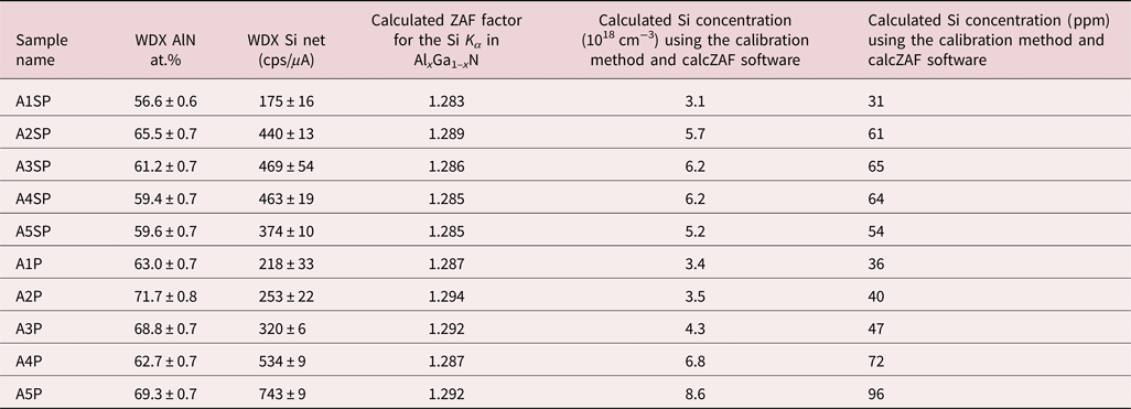
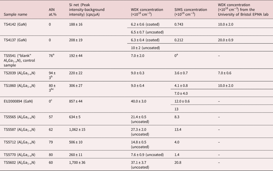
A range of Si-doped GaN and AlxGa1–xN samples, grown by MOCVD by different groups, were used to clarify the best way to measure Si. GaN:Si material (sample EU2000894) was provided by IQE Europe Ltd. A series of AlxGa1–xN samples with different crystal polarities and different AlN contents was provided by the Tyndall Institute. These AlxGa1-xN samples included polar-oriented [0001] (samples AP, BP, CP) and semipolar-oriented layers [112-2] (samples ASP, CSP). More details on the growth of the AlxGa1–xN:Si layers from the Tyndall Institute are given elsewhere (Li et al., Reference Li, Sadler and Parbrook2013; Dinh et al., Reference Dinh, Alam and Parbrook2016a, Reference Dinh, Pampili and Parbrook2016b; Pampili et al., Reference Pampili, Dinh, Zubialevich and Parbrook2018; Spasevski et al., Reference Spasevski, Kusch, Pampili, Zubialevich, Dinh, Bruckbauer, Edwards, Parbrook and Martin2021). Samples labeled TS are AlxGa1–xN layers with various AlN contents and crystal polarities grown at Technische Universität Berlin (Knauer et al., Reference Knauer, Kueller, Zeimer, Weyers, Reich and Kneissl2013; Kusch et al., Reference Kusch, Li, Edwards, Bruckbauer, Sadler, Parbrook and Martin2014; Mehnke et al., Reference Mehnke, Trinh, Pingel, Wernicke, Janzén, Son and Kneissl2016; Foronda et al., 2020). The “blank” AlxGa1–xN TS5541 was grown with no Si doping and quickly shipped in a sealed container filled with N2 gas in order to minimize contamination and on receipt it was immediately placed under vacuum within the EPMA chamber. Information on the three sets of samples is given in Tables 1 and 2. Attempts were made to remove inherent surface contamination by oxygen plasma cleaning treatments. Traditionally, plasma cleaning is employed to remove hydrocarbon contamination (Donovan & Rowe, Reference Donovan and Rowe2005). Apart from contamination, the samples can also suffer from oxidation. To investigate the effect of oxidation of the Si standard, cleaning with HF solution was employed.
Table 1. Reference GaN and AlxGa1–xN Samples for Which Independent Measurement of the Si Concentration Is Available.

a Sample TS5541 has not been measured by SIMS, but it was grown undoped, so the SIMS concentration is assigned to be 0; AlN at.% as estimated from the growth conditions.
b From Kusch et al. (Reference Kusch, Mehnke, Enslin, Edwards, Wernicke, Kneissl and Martin2017).
c Samples TS1860 and EU2000894 were measured by two of the three SIMS companies.
Table 2. List of AlxGa1–xN Samples for Which Independent Constraint on the Composition Is Not Available, Measured AlN at.% Using WDX and Si Kα Intensity Values Together with the Calculated Si Concentration (Crystal Orientation [0001] AxP, Orientation  $[ {11\bar{2}2} ]$ AxSP).
D-SIMS data were provided by three different companies: RTG Mikroanalyse GmbH Berlin (Jörchel et al., Reference Jörchel, Helm, Brunner, Thies, Krüger and Weyers2016), Loughborough Surface Analysis Ltd. (using a Cameca 7f), and Evans Analytical Group (EAG). All samples were analyzed in a depth profile mode, using areas typically 100 × 100 μm. RTG used ion-implanted AlGaN samples to produce absolute and relative sensitivity factors for Si in AlGaN, with further details given in Jörchel et al. (Reference Jörchel, Helm, Brunner, Thies, Krüger and Weyers2016). The same approach was used for data from Loughborough. EAG used a proprietary method that calculates the change in sensitivity factors with respect to the AlN fraction in AlGaN.
WDX measurements were performed in the EPMA with the incident electron beam normal to the sample surface, and an acceleration voltage of 10 kV which is sufficient to efficiently excite the selected X-ray lines. Under these conditions, the electron interaction volume is kept within the first 500–800 nm of the AlxGa1–xN layer according to Monte Carlo simulations using CASINO software (Drouin et al., Reference Drouin, Couture, Dany, Tastet, Aimez and Gauvin2007) and dependent on the AlN molar content. In all samples, the interaction volume is contained within the top most AlxGa1–xN layer. The beam current was 40 nA for analysis of the major elements (Al, Ga, N) and increased to 400–500 nA for the minor elements. The beam was defocussed to 10 or 20 μm to improve sample averaging and avoid damaging the sample. The samples and standards were carbon coated to remove charging effects, with a thickness of approximately 15 nm [as determined by the interference-color method of Kerrick et al. (Reference Kerrick, Eminhizer and Villaume1973)]. This becomes increasingly important for AlN-rich AlxGa1–xN for which the conductivity decreases. Measurements were also performed on two of the GaN:Si sample without coatings (and using uncoated standards) to confirm that the coating was not a source of Si.
According to best practice for trace analysis, the pulse height analysis (PHA) parameters (such as voltage window, baseline, electronic bias, and gain on the detector) were adjusted before measuring the Si Kα peak, using counter energy distributions of the peak on a pure Si standard with a beam current of 20 nA (Reed, Reference Reed2002). Si has the tendency for a peak shift due to valence and coordination (Fournelle, Reference Fournelle2006), but in our case, the shifts in the Si Kα peak position between pure Si standard and the unknown samples were insignificant. The differential mode was employed simply to exclude noise peaks and no higher-order interferences were observed in the region of the Si Kα peak (Geller & Herrington, Reference Geller and Herrington2002; Zhang et al., Reference Zhang, Koepke, Wang, Wolff, Wilke, Stechern, Almeev and Holtz2016).
In this paper, two methods were employed for checking the presence of Si dopants: qualitative and quantitative measurement. In the qualitative scan, the information on the element concentration is present in the height of the peak, extracted as peak maximum minus interpolated background. For the quantitative measurements, the EPMA's standard ZAF correction procedure was used in the usual way to determine the Si concentration and the results are included in Table 1. The quantitative procedure improves counting statistics due to the extended time spent acquiring peak and background X-rays, compared with the qualitative scan. The concentration of the major elements is quantified using the ratios of the background-corrected peak intensities for the sample to the corresponding ones obtained from AlN, GaN, and Si standards (k-ratios). Signals were acquired for 60 s on the peak positions and for 30 s on the background positions with a beam current of 20 nA. Ga Lα and Al Kα signals were recorded using a TAPH crystal (thallium acid phthalate, 100 mm Rowland circle), while for the N Kα signal, a synthetic layered LDE1L crystal (140 mm Rowland circle) was used. For quantification of the minor element, the Si Kα X-rays were recorded using a large TAP crystal (140 mm Rowland circle). The measured intensities are corrected for differences in composition between standard and specimen using the standard ZAF correction procedures in the JEOL EPMA software. The ZAF method consists of corrections for atomic number (Philibert-Tixier method), absorption (Philibert method), and fluorescent excitation (Reed method). The low silicon concentrations necessitate a separate measurement routine to that for the major elements, due to different requirements for the counting statistics between the major and minor elements (Sato et al., Reference Sato, Mori, Takakura and Notoya2007). Therefore, to improve counting statistics, longer measurement times and higher currents were employed: 400–500 nA, and 360 and 180 s counting times for the peak and background, respectively. The accelerating voltage and measurement positions were kept unchanged in order to ensure that the data for the silicon and major elements will refer to the same volumes within the sample. Unlike an EDX detector, WDX spectrometers record only one wavelength at a time so there is no risk of oversaturating the detector with major element counts when measuring silicon with high current. With the new measurement condition, the counting statistics were significantly improved for silicon and the counting error was reduced to 1–3% relative, with detection limit (DL) reduced to 1 ppm. Despite the smaller errors in the silicon signal, the final silicon concentration in the sample still resulted in higher concentrations [(0.6–4) × 1019 cm−3 levels] than expected when compared with SIMS data available for the same samples.
In order to check the accuracy of measured results, an inter-laboratory study was conducted and some samples were also measured on the EPMA (JEOL JXA-8530F) at the University of Bristol.
Results and Discussion
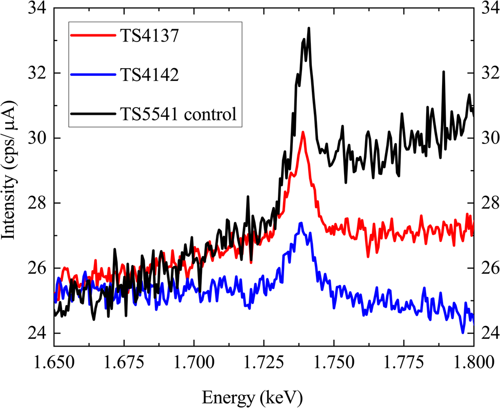
In order to test the detection limit of approximately 10 ppm (1σ), which corresponds to concentrations of 1018 cm−3 of Si in GaN, we performed WDX measurements on two GaN: Si samples (TS4142 and TS4137) with low silicon contents that were also characterized by SIMS (Table 1), and on one “blank” AlxGa1–xN sample TS5541. Figure 2 shows long qualitative WDX scans (dwell time 12 s, 505 points, total time: 1 h 36 min), which were performed to check for the existence of the Si Kα peak. A Si peak is clearly visible above the background level in all of the above-mentioned samples (even in the “blank” sample, referred from now on as a control sample) and much greater than error/detection limit. We conclude that sample TS5541 is not actually blank and has accrued Si either during growth or in the time before measurement. From the qualitative scans, it is also possible to conclude that there are no signs of any interference close to the Si Kα peak that could be a serious source of error in quantitative microanalysis and that the peak position is the same in the tested samples (Donovan et al., Reference Donovan, Snyder and Rivers1993). There are differences in the shape of the background for the samples shown in Figure 2, with the main difference being the high Al content in TS5541 which could be responsible for the increased background on the high-energy side for this sample.

Fig. 2. Long qualitative scan (dwell time 12 s) for the Si Kα peak from GaN:Si samples: TS4142 (blue), TS4137 (red), and AlxGa1–xN control sample TS5541 (black) using a TAPL crystal at 10 kV, 400 nA (100 nA for the control sample).
Since the SIMS measurements (for the GaN samples) gave values below or close to the detection limit, the silicon doping should have been unmeasurable in these cases. However, the WDX data show clear Si X-ray peaks and high apparent Si content (>6 × 1018 cm−3 compared with <7 × 1017 cm−3 from the SIMS value in Table 1). Furthermore, the WDX analysis returned a similar value for Si concentration from the control sample. Measurements performed at the University of Bristol for GaN samples (TS4142 and TS4137, Table 1) gave similar Si concentrations (×1.6 and ×2 higher, respectively). A different set of analytical conditions was used for the measurement, with a 400 nA current and 10 μm spot size. The above results appear to confirm that the samples are contaminated with Si in a way that would prevent convergence of the WDX and SIMS results by any simple adjustment of the analysis conditions. Attempts were, therefore, made to remove the contamination by cleaning treatments. Ex situ plasma cleaning did not result in any conclusive change when comparing Si content before and after cleaning (not shown).
Another possible reason for high Si values could be the existence of surface layers of native oxide formed on the standards. Oxidation of the standard will reduce the standard intensity due to the native oxygen layer and cause an overestimate of the concentration in the unknown (Merlet & Llovet, Reference Merlet and Llovet2012). The silicon standard will form native layers of oxygen on the surface. Therefore, cleaning in HF solution was employed to remove the oxide layer from the Si standard. Qualitative scans around the Si peak were performed before and after cleaning (not shown), and Si Kα intensity data were acquired on the Si standard before and after the cleaning to check the difference (Table 3).
Table 3. Si Kα Intensities Acquired for Pure Si Standard, Before and After Removal of Native Oxide Layer.
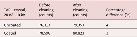
Table 3 shows that removal of the oxidation layer from the standard did not produce any significant changes (only 3–4%) in the intensity of Si Kα peak. We can assume that the native oxygen layer was thinner than 10 nm (Carpenter, Reference Carpenter2008).
Thus, as far as we can tell, cleaning treatments did not remove possible Si contamination and that oxidation of the sample or standard is not the reason for the large discrepancy between SIMS and WDX results. The data measured from two GaN:Si samples, with and without C-coating, confirm that the C-coat is not the source of extra Si.
After cleaning the Si standard, calibration data was acquired from it using a very low current of 1 nA in order to reduce the count difference between the standard and unknown trace element. This did not result in any difference in the measured concentration for the trace element when compared with calibration data acquired with 20 nA. Subsequently, all calibration data are acquired with a lower beam current of 20 nA compared with the 500 nA employed to measure Si in the unknowns, in order to avoid detector oversaturation. In doing this, we have relied on the current measurement system scaling linearly from 20 to 500 nA.
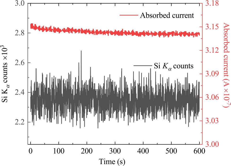
Due to the long measurement time and high currents used for the silicon analysis, the instrumental and sample stability need to be checked (Hughes et al., Reference Hughes, Buse, Kearns, Blundy, Kilgour and Mader2019). A sample will generally be stable during analysis with usual operating conditions (10–100 nA), but the high currents (hundreds of nA) required for trace-element analysis may cause it to degrade (Carpenter et al., Reference Carpenter, Counce, Kluk and Nabelek2002). It is necessary to assess if the samples are stable during measurement time due to potential charge build-up, heating or radiation damage. This was assessed by monitoring the count rate for Si Kα in one of the calibration samples at the same time as the absorbed current. Figure 3 shows that the silicon signal remains stable during the long counting times and there is only a very slight decrease of the absorbed current (0.3%). Since the measured absorbed current is not showing a significant drop or oscillations, it implies that the electrical properties of the coating are sufficient. The time scan was performed with a 10 μm defocused beam to simulate more extreme conditions, while the quantitative analysis sometimes used a beam diameter of 20 μm in order to minimize any absorbed current instability (Jercinovic & Williams, Reference Jercinovic and Williams2005).

Fig. 3. Time scan for Si Kα in the GaN:Si calibration sample under “trace analysis” electron-beam operating conditions showing a constant Si Kα count rate and absorbed current as a function of time, showing only minor change in the absorbed current during long counting times.
The results of all the tests described so far lead us to propose that the best solution for using WDX for the accurate measurement of doping in AlxGa1–xN samples is to generate a calibration relation using samples also characterized by D-SIMS. The results listed in Table 1 are plotted in Figure 4 and show that the Si net intensity value (peak minus background) does not go below about 200 cps/μA even for the samples with very low Si contents, which we attribute to surface contamination with Si (samples TS4142, TS4137, TS5541). These samples (marked by the gray circle) are thus considered not suitable for calibration and we propose a calibration relation for Si concentrations down to a lower limit defined by an Si net value of 200 cps/μA. Prior to generating this line, the impact of the host material must be accounted for as these samples consist of AlxGa1–xN with different AlN% contents (Table 2).
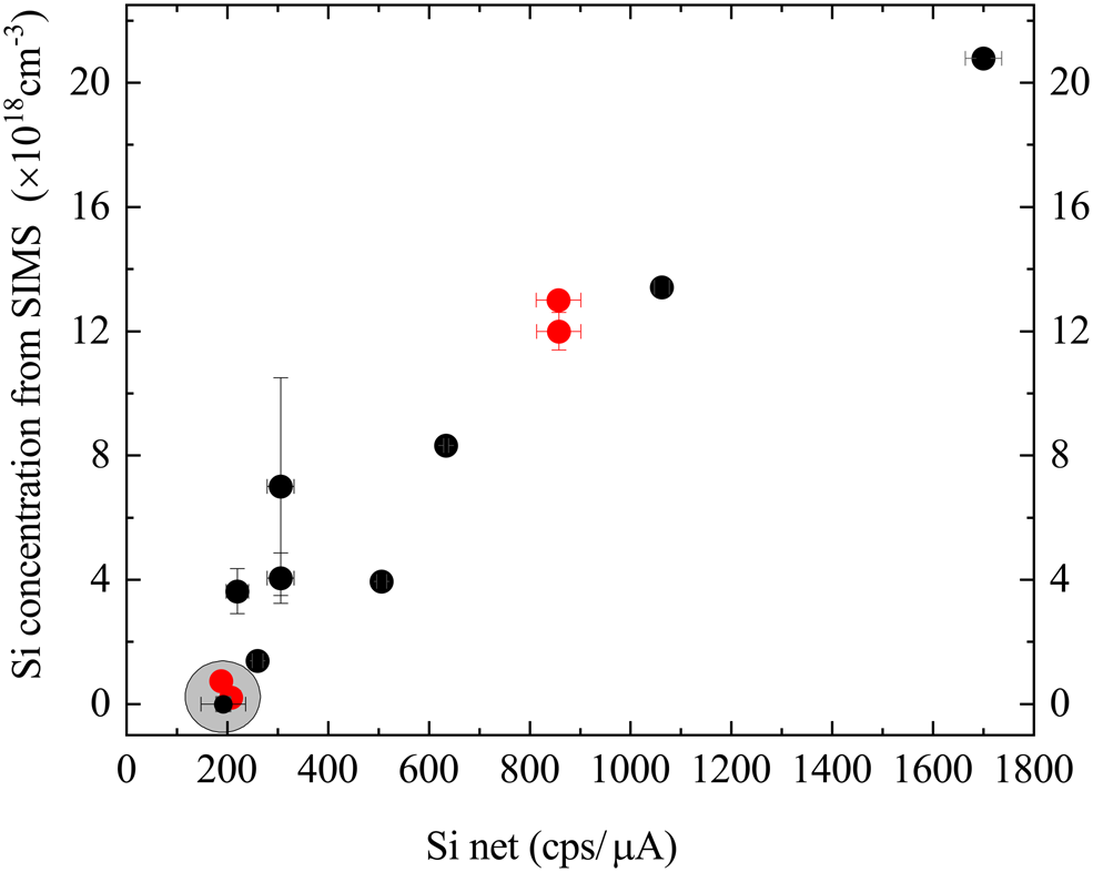
Fig. 4. Correlation between Si intensity measured by WDX and the concentration from SIMS data for GaN (red points) and AlxGa1–xN (black points) samples.
The change in matrix correction (ZAF correction) for Si for different AlN contents was estimated using the stand-alone CalcZAF software (Donovan et al., Reference Donovan, Pinard and Demers2019), as plotted in Figure 5. The different correction procedures available in CalcZAF software did not produce a noticeable difference in the correction factors.
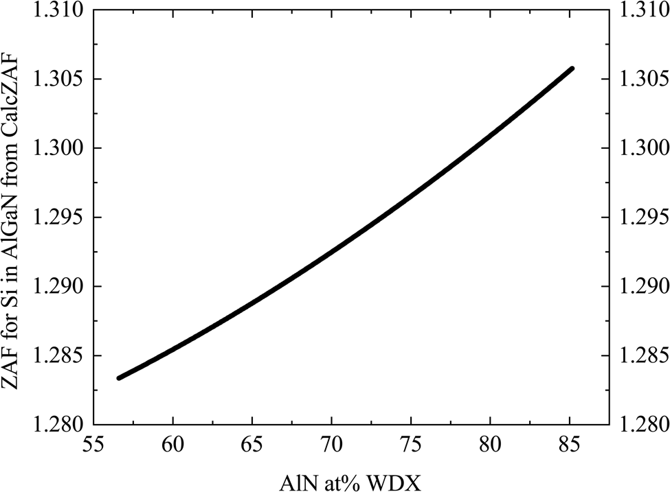
Fig. 5. Plot of the calculated matrix correction (ZAF correction) from elemental Si against AlN at.% as measured by WDX for each of the AlxGa1–xN samples.
The calculated ZAF parameters are then used to adjust all the D-SIMS calibration points to the effective value for a GaN host, as shown in Figure 6. This resulting calibration relation allows the Si content to be estimated in samples of all AlxGa1–xN compositions by measuring the Si intensity, then using the GaN calibration curve with the appropriate ZAF correction.
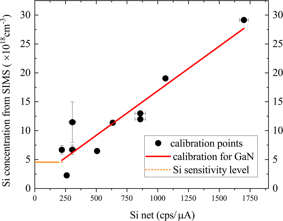
Fig. 6. Calibration relation with all the points representing Si intensity in GaN (For the AlxGa1–xN points, the Si concentration from D-SIMS is converted to its equivalent for GaN using calcZAF software). The orange dotted line represents the Si sensitivity level for GaN.
This process is illustrated using the series of AlxGa1–xN samples listed in Table 2. The measured intensity values, Si net (cps/μA), are adjusted to the effective Si net values for GaN, using the ZAF correction procedure, and these are then converted to Si concentration using the calibration curve. The calculated Si concentrations in AlxGa1–xN are plotted in Figure 7, which also shows the calibration line for GaN for comparison. This method enables the Si concentration in AlxGa1–xN samples of any composition to be estimated by measuring the Si intensity. For samples with Si net ≤200 cps/μA (e.g. sample A1SP), the equivalent Si concentration is set to the sensitivity limit of 35 ppm, which corresponds to concentrations ranging from 2.4 × 1018 cm−3 for AlN or 4.6 × 1018 cm−3 for GaN, calculated from the calibration curve in Figure 6.
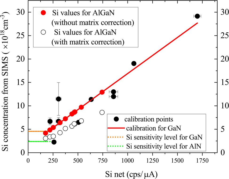
Fig. 7. Values for Si concentration in AlxGa1–xN:Si layers plotted against the measured Si net signal. The line is the calculated calibration for GaN:Si and the points differ from this line according to the amount of AlN contained in the host material.
Figure 8 plots the calculated Si concentrations against the disilane to group III ratios (Si2H6/III ratios) (Dinh et al., Reference Dinh, Alam and Parbrook2016a, Reference Dinh, Pampili and Parbrook2016b; Pampili et al., Reference Pampili, Dinh, Zubialevich and Parbrook2018). In MOCVD growth, the group III atoms are introduced via metal precursors in the form of organic compounds such as trimethylgallium and trimethylaluminium, while ammonia is the nitrogen source. Doping can be obtained by introducing into the reactor dopant-containing gases, such as disilane (Si2H6) (Pampili & Parbrook, Reference Pampili and Parbrook2017). The measured Si concentrations for the semipolar ASP samples increase linearly with the Si2H6/III ratio up to a saturation point of 2.3 × 10⁻⁴ Si2H6/III. The saturation point is consistent with a previous report from Dinh et al. (Reference Dinh, Alam and Parbrook2016a), where the carrier concentration and mobility of semipolar layers were observed to reach a maximum at a similar Si2H6/III ratio. The AP series exhibits an almost linear increase of Si with disilane flow rate.

Fig. 8. Si concentration of the AlxGa1–xN-doped layer as a function of disilane to group III ratio, as evaluated by WDX. The solid lines provide guides to the eye.
Summary
The use of WDX spectroscopy for the measurement of silicon-doping levels in wide band-gap AlxGa1–xN layers is demonstrated in a commercially available EPMA instrument. A previously reported limitation with over-estimates of the Si contents was thoroughly investigated and was assigned to surface contamination. An analytical routine was introduced for measuring the trace Si levels, consisting of separate measurement of Si with high current and long counting times followed by calibration using D-SIMS measurements. By measuring silicon intensities and using a calibration curve fit method using the D-SIMS data along with calculated ZAF correction values, it was possible to determine doping levels of order (3–10) × 1018 cm−3 in AlxGa1–xN layers with varying AlN contents and polarity. The highest values of Si incorporation were observed for polar samples (100 ppm), while saturation of Si incorporation was seen for semipolar samples at a high Si/III ratio. The advantages of the WDX approach include high lateral spatial resolution and the ability to determine the alloy composition of the major elements, such as Al, Ga, and N, at the same time as the doping levels. The standards used in WDX analysis are more accessible compared with ion-implanted standards required for the SIMS analysis. Apart from the quantitative abilities of the EPMA instrument, another major advantage in the examination of the semiconductor alloys is the correlation of WDX data with other microscopy techniques such as CL and ECCI as well as the high-resolution mapping capabilities.
Acknowledgments
The authors thank Dr. Trevor Martin from IQE Europe Ltd., for providing additional GaN:Si samples, and to Drs. Vitaly Zubialevich, Pietro Pampili, and Duc Dinh from Tyndall National Institute for providing additional AlGaN:Si samples. We acknowledge Alison Chew of Loughborough Surface Analysis Ltd. for provision of D-SIMS measurement and discussion of the results. We thank Dr. Gunnar Kusch for useful discussion and advice. We thank Dr. Stacey Laing from the Department of Pure and Applied Chemistry, University of Strathclyde, for performing plasma cleaning of the samples. We would also like to show our gratitude to Mr. James Sweeney and Dr. Ian Watson from the Institute of Photonics, University of Strathclyde, for cleaning the samples with HF solution. This work was supported by the EPSRC project EP/N010914/1, “Nanoanalysis for Advanced Materials and Healthcare,” by the EU-FP7 programme “ALIGHT,” Science Foundation Ireland through SFI/10/IN.1/I2993 and Irish Photonic Integration Centre (SFI/12/RC/2276_2), and the European Space Agency. All data underpinning this publication are openly available from the University of Strathclyde KnowledgeBase at: https://doi.org/10.15129/aa61c668-99ca-4802-9013-ff5f15409240.


 Open access