


I. INTRODUCTION
In the past decade, transition metal oxides (TMOs) have gained significant attention due to their outstanding catalytic, ferroelectric, superconducting, and optical properties. Such a diverse array of properties has resulted in their use in various applications such as heterogeneous catalysis, sensors, solar cells, and batteries. One of the unique features of TMOs is the dependence of their band gaps, and hence their electrical conductivities, on stoichiometry. TMO stoichiometry can be modulated from the insulating (e.g., V2O5, ∼2.2 eV) to the semiconducting (e.g., VO2, ∼0.7 eV) to the metallic state (e.g., VO, no gap) by changing the concentration of anionic or cationic vacancies in the lattice. Both experimental and theoretical studies have shown that many of the unique properties of metal oxides arise as a result of the complex surface chemistry and the presence of lattice vacancies, which significantly perturb their electronic structure. Reference Henrich and Cox1–Reference Wendt, Schaub, Matthiesen, Vestergaard, Wahlström, Rasmussen, Thostrup, Molina, Lægsgaard, Stensgaard, Hammer and Besenbacher3 Studies on both pure and reduced anatase TiO2 and CeO2 surfaces showed that nonstoichiometric or reduced surfaces have an increased number of surface and subsurface oxygen vacancies. Reference Bikondoa, Pang, Ithnin, Muryn, Onishi and Thornton4–Reference Esch, Fabris, Zhou, Montini, Africh, Fornasiero, Comelli and Rosei6 These sites act as low energy binding sites for absorption of O2 and H2O molecules, and are critical to the enhancement of catalytic activity. Reference Epling, Peden, Henderson and Diebold7–Reference Wu, Selloni, Lazzeri and Nayak10 Thus, the ability to control the density and nature of defects such as vacancies is crucial not only for tailoring catalytic performance, but also for further expanding the scope of oxide-based devices.
TMOs have been grown by a number of techniques such as solvo-thermal synthesis, Reference Son, Wei, Cobden, Cao and Xia11 sol–gel techniques, Reference Della Gaspera, Guglielmi, Martucci, Giancaterini and Cantalini12 physical vapor deposition techniques such as radiofrequency (RF) sputtering Reference Suhail, Rao and Mohan13,Reference Padmini, Taylor, Lefevre, Nagra, York and Speck14 and e-beam evaporation, Reference Nemetz, Temmink, Bange, Cordoba de Torresi, Gabrielli, Torresi and Hugo-Le Goff15 and chemical vapor deposition (CVD) including metal-organic CVD (MOCVD) Reference Jones16 and thermal CVD. Reference Luyo, Ionescu, Reyes, Topalian, Estrada, Llobet, Granqvist and Heszler17–Reference Lu, Zhai, Zhang, Shen, Yuan, Hu, Gong, Chen, Gao, Zhou, Tong and Wang20 Synthesis techniques such as hydrothermal or sol–gel deposition are advantageous for low temperature synthesis of nanostructures, but often result in the inclusion of undesired precursor ions or solvent molecules that can have a significant impact on the electrical properties of the TMOs. Reference Chirayil, Zavalij and Whittingham21 This is the case for films deposited using MOCVD, which contain a significant amount of pyrolysis products such as carbon. Both RF sputtering and e-beam evaporation techniques can give relatively pure films with a well-controlled composition, but the nature of deposition is mostly polycrystalline. Previous studies have shown that the hot wire CVD (HWCVD) technique, which consists of reacting oxygen with a hot filament of the respective transition metal, can successfully be used for synthesis of various metal oxides. Reference Lee, Deshpande, Parilla, Jones, To, Mahan and Dillon22–Reference Chakrapani, Thangala and Sunkara24 The main advantages of this technique are the ability to grow relatively pure films without the use of extraneous solvents and counter ions and the ease with which single crystalline nanostructures can be deposited over a large surface area.
In this paper, we show that the HWCVD technique is well suited for controlling the morphology, stoichiometry, and composition of different metal oxides. Molybdenum, tungsten, and vanadium were chosen as the model systems for the synthesis of binary oxides, although the methodology is applicable to other TMOs as well. Next, we show that this same technique can be extended to the deposition of ternary oxides as well. Nickel molybdenum oxide (NiMoO4) was chosen for the proof-of-concept synthesis.
II. SYNTHESIS AND METHODS
Synthesis of various metal oxides was done in a custom-built HWCVD reactor. The technique involves resistively heating a metal wire, the oxide of which we are interested in, close to its melting point. The feed gases consist of either pure oxygen or a mixture of argon, oxygen, and water vapor at partial pressures ranging from 0.1 Torr to 10 Torr. The reaction of oxygen with the hot metal filament results in the formation of the respective metal oxide on the cooler parts of the reactor. Deposition was carried out on various substrates such as fluorinated tin oxide (FTO), silicon, or quartz wafers at filament temperatures in the range of 1000–1950 K and substrate temperatures in the range of 550–823 K. The substrates were ultrasonically cleaned in ethanol and dried under pure nitrogen flow before being used for deposition. The substrate and filament temperatures were modulated, as were the gas phase composition and flow rate, to control the density, morphology, and stoichiometry of the nanostructures. Water vapor was used as the source for hydrogen in the gas phase, and its presence typically resulted in reduced or sub-stoichiometric phases for both n- and p-type metal oxides. Measurements of filament temperatures using an optical pyrometer showed significant errors. The measured filament current during deposition, however, was quite stable during various runs. The power delivered to the filament was calculated from the applied voltage and the measured current, and was used as the indicator of filament temperature. In some cases, the resistance of the wire changed with continuous use (usually between 6–7 runs) as a result of sputtering. This led to small changes in the delivered power. R was used as an indicator for filament temperature in these instances. Thus, increasing values of R and P indicate increasing filament temperature.
Ternary TMOs were synthesized by wrapping the short loops of the two respective metal wires alternatively in a series connection. Shorter loops of the metal wire ensured good mixing of the two metal oxide vapors to enable uniform deposition instead of preferential deposition of the binary oxide.
The as-synthesized nanostructures were characterized by a variety of spectroscopy techniques. The morphology, composition, and phase change of the nanowires were examined by using a scanning electron microscope (SEM, Carl Zeiss Supra SEM, Carl Zeiss, Oberkochen, Germany) equipped with an energy dispersive analyzer, powder x-ray diffraction (Bruker, D8 Advance, Bruker, Karlsruhe, Germany), and Raman Spectroscopy (Horiba Labram UV Raman and PL spectrometer, Horiba Scientific, Edison, New Jersey). The optical absorbance of the sample was measured both in the transmittance and reflectance mode using a Shimadzu 3600 UV–Vis–NIR spectrophotometer (Shimazdu Corporation, Tokyo, Japan) over the wave length of 200–3000 nm to determine the band gap of the material. Using the measured spectral transmittance (T S) and the film thickness (d), the optical absorption coefficient (α) was evaluated using the relationship Reference Pankove25 :
 $$\alpha = {1 \over d}{\it ln} \left[ {{{1 - R_s} \over T_s}} \right]\quad ,$$
where R S is the reflectance from the sample, and was assumed to be zero when experiments were done in the transmission mode. The optical band gap was determined using the Tauc formula:
 $$\alpha h\nu = \beta {\left( {h\nu - {E_{\rm{g}}}} \right)^n}\quad ,$$
where β is a constant and n is equal to 2 or ½ for the allowed indirect or direct transitions, respectively. An extrapolation of the tangent line to the linear portion of the curve to the x-axis gives the value of the optical band gap.
Ultraviolet photoelectron spectroscopy (UPS, Phi Versaprobe XPS/UPS System, PHI Electronics, Chanhassen, Minnesota) was performed to determine the effect of nonstoichiometry on the surface electronic states of the oxide. Samples were excited using a He I (hν = 21.1 eV) excitation line. All surfaces were cleaned before measurements by Ar-ion sputter etching. The ultimate resolution of the UPS data is limited by the natural line width of the excitation source at 0.1 eV. All spectra were recorded using normal emission and at a constant analyzer energy of 2.5 eV. The surface of the sample was grounded to negate any charging effects during the photoelectron spectra acquisition. A sputter-cleaned polycrystalline gold foil served as the reference for calibration of the energy scale.
III. RESULTS AND DISCUSSION
Oxides of many different transition metals were grown using the HWCVD technique. Representative top-down SEM images are shown in Figs. 1(a)–1(c). By tightly controlling the power supplied to the filament and the partial pressure of oxygen in the chamber, highly aligned, single crystalline nanowire arrays of the respective oxide could be grown on a variety of substrates such as FTO, Si, or glass. The nanowires were typically 5–10 μm in length with diameters in the range of 40–80 nm.

FIG. 1. Top down SEM images of the as-synthesized, vertically aligned nanowire arrays on the FTO substrate of (a) WO3, (b) MoO3, and (c) V2O5.
A. Control of the morphology
Control of the morphology of the 1D nanostructure is highly desirable in many applications for modulating the transport and electrical properties. For example, vertically aligned nanowires are highly desirable for many solar cell applications for fast and direct electron transport to the back contact.
Reference Chakrapani, Thangala and Sunkara24
The high diffusion coefficient of ions such as Li along certain crystallographic directions means nanostructured platelets are highly efficient for Li ion transport in battery applications.
Reference Su, Dou and Wang26
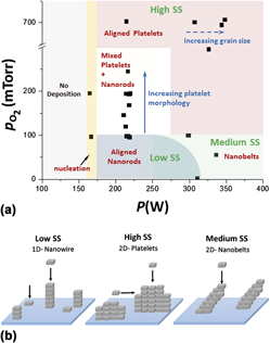
In this regard, HWCVD is well suited for tuning the morphology of metal oxide nanostructures. Molybdenum oxide (MoO3) was chosen as the model system. Samples with different morphologies were grown under different filament temperatures and partial pressures of oxygen. In some cases, argon or water vapor was added to the chamber to control the growth rate. The results of these experiments are plotted as a morphological phase diagram in Fig. 2(a) as a function of the filament power (P) and partial pressure of supplied oxygen $\left( {{p_{{{\rm{O}}_2}}}} \right)$
. Various regions in the phase diagram are highlighted with different colors based on the observation of varying types of morphologies in the final deposit. It was observed that low-pressure, low-power conditions resulted in the nanowire growth. High pressures of oxygen and high power favored the growth of thin platelets that in some instances grew several tens of microns in width. Under intermediate conditions of power and pressure, a mixture of nanowire and platelet deposition was obtained. A belt-like morphology was obtained when deposition was carried out under low oxygen concentrations and high filament temperatures or power. SEM images of these structures are shown in Figs. 3(a)–3(l).
$\left( {{p_{{{\rm{O}}_2}}}} \right)$
. Various regions in the phase diagram are highlighted with different colors based on the observation of varying types of morphologies in the final deposit. It was observed that low-pressure, low-power conditions resulted in the nanowire growth. High pressures of oxygen and high power favored the growth of thin platelets that in some instances grew several tens of microns in width. Under intermediate conditions of power and pressure, a mixture of nanowire and platelet deposition was obtained. A belt-like morphology was obtained when deposition was carried out under low oxygen concentrations and high filament temperatures or power. SEM images of these structures are shown in Figs. 3(a)–3(l).

FIG. 2. (a) Morphological phase diagram of MoO3 grown under different conditions of filament power (P) and partial pressure of oxygen $\left( {{p_{{{\rm{O}}_2}}}} \right)$
in the reactor. Regions of varying morphology are differentiated with varying background color. Regions of high, medium, and low gas phase supersaturation are indicated as “high SS”, “medium SS,” and “low SS”, respectively, (b) Schematic of the growth process under different conditions of supersaturation.
$\left( {{p_{{{\rm{O}}_2}}}} \right)$
in the reactor. Regions of varying morphology are differentiated with varying background color. Regions of high, medium, and low gas phase supersaturation are indicated as “high SS”, “medium SS,” and “low SS”, respectively, (b) Schematic of the growth process under different conditions of supersaturation.

FIG. 3. SEM images of MoO3 grown under different conditions of filament power and partial pressure of oxygen in the reactor, (a & b) high O2, high power; (c–h) fixed medium power, and decreasing oxygen partial pressure; (i) low O2, high power; (j–l) High O2, increasing high power.
B. Model for nanostructure growth
A number of different mechanisms have been proposed for the growth of nanostructures of various morphologies, including vapor–liquid–solid (VLS), Reference Morales and Lieber27,Reference Wu, Yan, Huang, Messer, Song and Yang28 vapor–solid (VS), Reference Dong, Gushtyuk and Jiao29 solution–liquid–solid (SLS), Reference Yu and Buhro30 oxide-assisted growth, Reference Zhang, Lifshitz and Lee31 and defect-induced growth mechanisms. Reference Sears32 No additional metals were used as the catalyst for nanostructure growth, and both SEM and transmission electron microscopy (TEM) images (not shown) did not show the presence of any metal catalyst at the tips of the nanostructure. Thus, the catalyst-induced VLS or SLS mechanism is not the governing mechanism. Further, high-resolution images showed no built-in screw dislocations in the as-deposited samples, so it is unlikely that defect-induced nucleation plays any role in the growth process. It is most likely that the growth of metal oxide nanostructures follows the evaporation-condensation or VS mechanism. In a typical VS process, the vapor species are first generated by evaporation and chemical reaction. For synthesizing metal oxides, it is believed that the important intermediate species required for growth is a reduced phase of metal oxide vapor, such as MoO2 or WO2. Thus, the first step is either the reaction of a hot metal filament with oxygen to form the reduced metal oxide vapor or the formation of a fully oxidized metal vapor (MoO3 or WO3) followed by its subsequent reduction in the gas phase to form the reduced oxide vapor. The intermediate reacting species are then transported and condensed onto the surface of a solid substrate that is at a much lower temperature. The condensed nuclei then undergo oxidation to form the fully oxidized phase of the metal oxide.
The most important parameter that controls the morphology of nanostructure growth is the degree of supersaturation of the reaction intermediates that are responsible for nucleation and growth at the prevailing experimental conditions. Reference Morales and Lieber27,Reference Hsu and Lu33,Reference Xia, Yang, Sun, Wu, Mayers, Gates, Yin, Kim and Yan34 Gas phase supersaturation, SS, is defined as Reference Cao and Wang35
 $$SS = {{p - {p_0}} \over {{p_0}}}\quad ,$$
where p is the partial pressure of the intermediate reacting species and p 0 is the equilibrium vapor pressure of the species over the solid substrate. The relative supersaturation associated with the principal growth forms (nanowires, bulk crystal, and powders) has also been documented. A low supersaturation is necessary for nanowire growth, whereas a medium supersaturation supports bulk crystal growth. At very high supersaturation, powders are formed by homogeneous nucleation in the vapor phase. Reference Xia, Yang, Sun, Wu, Mayers, Gates, Yin, Kim and Yan34 The lateral dimensions of the nanowires can be varied by controlling a number of parameters including supersaturation, nucleation size, and growth time. In all cases, the driving force for spontaneous nucleation is the reduction of Gibbs energy or chemical potential which occurs as a result of recrystallization or reduction in the supersaturation. For anisotropic growth such as the growth of nanowires, the growth rate of crystal facets in the longitudinal direction is much higher than in the axial directions. Although it is not well understood why growth rates in certain crystallographic directions are higher than others, several possible mechanisms have been suggested such as differences in the chemical potential along different crystallographic directions, presence of crystallographic defects such as screw dislocations, and the preferential accumulation of impurities in certain crystallographic facets. Reference Cao and Wang35
In HWCVD, supersaturation at the substrate can be estimated by considering the magnitude of the filament temperature and the difference between the filament and substrate temperatures. The rate of sublimation of metal oxide species from the filament is controlled by the magnitude of the filament temperature (or power), and it increases with increasing filament temperature. The equilibrium vapor pressure (p 0) over the substrate also increases with temperature, and is primarily determined by the substrate temperature. When both filament temperature and the partial pressure of oxygen in the chamber are low, the concentration (or partial pressure, p) of metal oxide vapors in the gas phase is low. This results in low supersaturation over the substrate. This region is marked as “Low SS” in Fig. 2(a). Conditions of low supersaturation preferentially favor growth of a nanowire morphology. See Figs. 2 and 3. Increasing partial pressure of oxygen in the chamber at constant filament power increases supersaturation. Figures 3(c)–3(h) shows SEM images of the MoO3 grown with increasing oxygen concentration. As is evident, increasing supersaturation [denoted by the solid vertical line in Fig. 2(a)] leads to a transition from pure 1D nanowire growth to a more mixed nanostructure growth consisting of nanowires and increasing 2D platelet growth. When the oxygen partial pressure in the chamber was 300 mTorr or higher, only 2D platelet growth was observed. At fixed high partial pressures of oxygen, increasing the power [denoted by the dashed horizontal line in Fig. 2(a)] results in high supersaturation and high concentrations of metal oxide vapor in the gas phase that are available to move downstream for deposition. In addition to the high supersaturation, which favors spontaneous crystallization, the relatively high substrate temperature provides substantial thermal energy and mobility to the atoms on the substrate so they can arrange into larger grains or domains of a similar orientation. This results in the formation of platelets with increasing grain size. This region is marked as “high SS” in Fig. 2(a). The corresponding SEM images of the deposition are shown in Figs. 3(j)–3(l). For an oxygen partial pressure of 700 mTorr, an increase in the filament power from 300 W to 700 W led to a progressive increase in the grain size of MoO3 platelets from 2 μm to 12 μm. In all cases, the deposition was vertically oriented, single crystal platelets with their (111) facets perpendicular to the substrate. The effect of supersaturation on the growth morphology is shown schematically in Fig. 2(b).
If the vapor travels to a moderately high substrate temperature zone, the supersaturation is intermediate. This is the case when deposition occurs at high power and low oxygen concentration. High filament temperature promotes the formation of intermediate gas phase species. However, the low oxygen concentration lowers the partial pressure of the metal oxide intermediate. The close proximity of the substrate to the hot filament causes an increase in the substrate temperature under high power conditions. This increases the equilibrium vapor pressure of the species over the substrate. The net effect of these three processes is that it results in values of supersaturation that lie in between the high and low SS values discussed previously. Medium SS conditions favor the growth of nanobelts that are several microns long with diameters in the range of 200–500 nm. See Fig. 3(i). Growth in this region is 2D, but with the characteristic growth features of deposits from both low SS and high SS regions. The high filament power results in the widening of the diameter from ∼60 nm (nanowire region) to ∼500 nm, which is indicative of substantial mobility of adatoms in the direction parallel to the substrates. On the other hand, lower oxygen pressure supports 1D growth along the axis perpendicular to the substrate. This leads to growth of nanobelts that are several microns long. The tip of the nanobelts shows a tapered structure, which could be a result of the high rate of metal oxide evaporation (or decomposition) at the surface caused by high substrate and filament temperature. A similar belt-like nanostructure growth has been observed for CdS grown via the VS mechanism by vaporizing CdS powders at high temperatures. Reference Zhang, Jiang and Zhang36 From all the above results, it can be concluded that the partial pressure of O2 predominantly determines the ratio of 1D to 2D growth, while the filament controls the extent of growth along the preferential direction.
C. Nature of reaction intermediate
Chemical reactions and the formation of intermediate compounds play an important role in the growth of nanostructures. The nature of reaction intermediates or precursors responsible for the growth of the metal oxide is not known. During metal oxide growth, decomposition reactions, formation of highly reactive radicals, and other side reactions can simultaneously occur due to the high filament temperature, and these must be taken into consideration. Experimental evaluation of the nature of intermediates is difficult, but theoretical calculations can provide important insight into their nature. However, for many intermediates and radicals, thermodynamic property data are not available. Theoretical calculations by Thangala et al. Reference Thangala, Vaddiraju, Bogale, Thurman, Powers, Deb and Sunkara23 on a limited number of possible species indicated that the free energy for the formation of WO2 is highly favorable, and may be the dominant gas phase intermediate. They performed equilibrium calculations considering gas-phase species consisting of O, O2, WO, WO2, W3O8, and WO3, and solid-phase species consisting of W, WO2, WO2.9, and WO3 for which data were available. At their experimental filament temperature of 1950 K, they found that the absolute equilibrium concentrations of WO2 gas-phase species were at least seven orders of magnitude more than those of WO and W3O8 gas phase species. They noted that the supersaturation of WO2 was much greater than that of WO3 under their experimental conditions, and hence the condensation of WO2 gas-phase species into solid WO2 was thermodynamically favored. Both WO3 and MoO3 share many properties that are similar, so it is likely that a reduced oxide of molybdenum, most likely MoO2, may be the key intermediate in the growth of MoO3.
For the growth conditions sampled in our chamber, it was observed that the addition of water significantly enhanced the rate of deposition. This indicates that hydrogen plays an important role in the formation of the key intermediate in the deposition reaction, and most likely promotes the formation of the reduced phase of the oxide such as MoO2 or WO2. The growth of metal oxides then occurs through a two-step reduction-oxidation process, where the reduced oxide is oxidized back to MoO3 or WO3 at the substrate. Hydrogen and water have previously been used for the growth of other binary oxides, such as MgO, Reference Yin, Zhang and Xia37 and a two-step process was proposed to explain the growth mechanism. In addition to hydrogen, carbon has also been used as a reducing agent for the reduction process. Lieber and co-workers Reference Yang and Lieber38 reported that the carbothermal synthesis of MgO nanowires follows a similar reduction-oxidation process, in which the reduction of MgO by carbon results in the formation of Mg vapors that is then transported to the growth zone, and oxidized to MgO at the substrate.
D. Control of stoichiometry
In addition to the morphology, stoichiometry of the metal oxide can be modulated by controlling the concentration of oxygen and water vapor in the gas phase as well as by controlling the filament power. For molybdenum and tungsten oxide, the change in the color of the samples was a direct indication of the changes in the stoichiometry of the final deposited products. For molybdenum oxide, the fully oxidized, stoichiometric form of MoO3 showed white coloration. With progressive deviation in stoichiometry from the fully oxidized MoO3, the samples showed increasing dark blue coloration with the formation of MoO3−x. The inset in Fig. 4(a) shows a photograph of samples synthesized with varying oxygen content. Figure 4(a) shows the ${p_{{{\rm{O}}_2}}} - R$
phase diagram, indicating the variation of color (stoichiometry) of the MoO3 deposit as a function of partial pressure of oxygen
${p_{{{\rm{O}}_2}}} - R$
phase diagram, indicating the variation of color (stoichiometry) of the MoO3 deposit as a function of partial pressure of oxygen $\left( {{p_{{{\rm{O}}_2}}}} \right)$
and resistance (R) of the hot filament, which was proportional to the temperature of the filament. Samples deposited at high
$\left( {{p_{{{\rm{O}}_2}}}} \right)$
and resistance (R) of the hot filament, which was proportional to the temperature of the filament. Samples deposited at high ${p_{{{\rm{O}}_2}}}$
(>500 mTorr) and high power (R > 5.6 Ω) were white, which indicated that they were stoichiometric MoO3. For a fixed power, increasing the gas phase concentration of oxygen resulted in deposition that showed a transition in color from dark blue to light blue to white. Growth at these conditions can be understood in terms of the growth model proposed earlier. Increasing concentration of oxygen not only increases supersaturation of reacting species but also promotes increased rate of oxidation of MoO2 nuclei to MoO3. Under relatively low power or resistance and oxygen-deficient conditions, the formation of reduced oxide (blue coloration) is promoted. At a fixed oxygen concentration, increasing the power promotes stoichiometric deposition. Several factors may contribute to this: high filament power may result in greater substrate temperatures, which enhance the rate of the oxidation reaction or lead to dissociation of oxygen and formation of more active oxygen species that promote the oxidation reaction step.
${p_{{{\rm{O}}_2}}}$
(>500 mTorr) and high power (R > 5.6 Ω) were white, which indicated that they were stoichiometric MoO3. For a fixed power, increasing the gas phase concentration of oxygen resulted in deposition that showed a transition in color from dark blue to light blue to white. Growth at these conditions can be understood in terms of the growth model proposed earlier. Increasing concentration of oxygen not only increases supersaturation of reacting species but also promotes increased rate of oxidation of MoO2 nuclei to MoO3. Under relatively low power or resistance and oxygen-deficient conditions, the formation of reduced oxide (blue coloration) is promoted. At a fixed oxygen concentration, increasing the power promotes stoichiometric deposition. Several factors may contribute to this: high filament power may result in greater substrate temperatures, which enhance the rate of the oxidation reaction or lead to dissociation of oxygen and formation of more active oxygen species that promote the oxidation reaction step.

FIG. 4. (a & b) Color map showing varying stoichiometry of (a) MoO3, and (b) WO3, synthesized under different conditions of oxygen partial pressure $\left( {{p_{{{\rm{O}}_2}}}} \right)$
and filament resistance (R). The insets in figures a and b show photographs of the as-grown samples with varying stoichiometry. The two dark blue WO3 samples shown in the left of the photograph were obtained when water vapor was present in the reaction chamber.
$\left( {{p_{{{\rm{O}}_2}}}} \right)$
and filament resistance (R). The insets in figures a and b show photographs of the as-grown samples with varying stoichiometry. The two dark blue WO3 samples shown in the left of the photograph were obtained when water vapor was present in the reaction chamber.
Similar to molybdenum oxide, stoichiometry of tungsten oxide was also modulated by controlling the concentration of O2, H2O vapor, and filament power. Completely oxidized, fully stoichiometric (WO3) samples were yellow in color. Progressive deviation from this stoichiometry (WO3−x) resulted in changes in the color of the sample from yellow to green to light blue and then finally to dark blue. Figure 4(b) shows the ${p_{{{\rm{O}}_2}}} - R$
phase diagram, where deposition under various conditions was carried out without the addition of water vapor to the reaction chamber. Similar to MoO3 phase diagram, high partial pressure of oxygen promotes the formation of stoichiometric oxide. Increasing the power at a fixed concentration (e.g.,
${p_{{{\rm{O}}_2}}} - R$
phase diagram, where deposition under various conditions was carried out without the addition of water vapor to the reaction chamber. Similar to MoO3 phase diagram, high partial pressure of oxygen promotes the formation of stoichiometric oxide. Increasing the power at a fixed concentration (e.g., ${p_{{{\rm{O}}_2}}} \sim 200$
mTorr) of oxygen, results in deposit that are more stoichiometric (blue to yellow), but further increase in the power results in deposits that are less stoichiometric (yellow to green). High filament and substrate temperatures may promote the rate of oxidation of WO2 to WO3 (yellow coloration), but very high powers may lead to high sputter rates, which lead to a greater oxygen deficiency in the gas phase and hence the formation of the reduced oxide (green–blue coloration). With the addition of water vapor in the gas phase, highly nonstoichiometric oxides could be obtained, as seen by the deep bluish-black coloration of the deposit. The inset in Fig. 4(b) shows the photograph of tungsten oxide samples of varying colors prepared under different growth conditions. The two dark blue WO3 samples shown in the left of the photograph were obtained with the addition of water vapor to the reaction chamber.
${p_{{{\rm{O}}_2}}} \sim 200$
mTorr) of oxygen, results in deposit that are more stoichiometric (blue to yellow), but further increase in the power results in deposits that are less stoichiometric (yellow to green). High filament and substrate temperatures may promote the rate of oxidation of WO2 to WO3 (yellow coloration), but very high powers may lead to high sputter rates, which lead to a greater oxygen deficiency in the gas phase and hence the formation of the reduced oxide (green–blue coloration). With the addition of water vapor in the gas phase, highly nonstoichiometric oxides could be obtained, as seen by the deep bluish-black coloration of the deposit. The inset in Fig. 4(b) shows the photograph of tungsten oxide samples of varying colors prepared under different growth conditions. The two dark blue WO3 samples shown in the left of the photograph were obtained with the addition of water vapor to the reaction chamber.
To evaluate the effect of nonstoichiometry on the structural, optical, and electronic properties, the tungsten oxide samples were characterized by XRD, UV–Vis absorption and UPS measurements. Figure 5 shows the XRD spectrum of four different tungsten oxide samples grown with various stoichiometries. It is clear from the figure that changes in the stoichiometry of the deposit leads to changes in the crystal structure. The yellow tungsten oxide nanowire showed primary peaks corresponding to a single crystal monoclinic WO3 phase with preferred orientation being [001]. In the presence of increasing water vapor in the reaction chamber, the deposition showed increasing deviation from stoichiometry. A bluish black deposit obtained with maximum concentration of water vapor during growth showed an XRD peak that matched well with reduced oxide WO2. The predominant diffraction peaks seen at 2θ values of 23.27 and 47.95 matched with the (111) and (141) hkl values of orthorhombic WO2 with the Pnma space group. Deposits with lighter blue coloration were identified to be monoclinic W18O49 (WO2.72) and monoclinic WO2.83. Raman spectra (not shown) of WO3 showed well-defined bands at 135, 274, 315, 715, and 808 cm−1, which corresponds to the monoclinic phase of tungsten oxide. The Raman peaks at 715 and 808 cm−1 correspond to the O–W–O bending modes and stretching modes. Reference Mwakikunga, Sideras-Haddad, Forbes and Arendse39 The peak at 274 cm−1 has previously been assigned to W4+ states. Reference Boulova, Rosman, Bouvier and Lucazeau40

FIG. 5. XRD of the as-grown tungsten oxide of varying stoichiometry obtained by controlling the filament temperature and partial pressures of oxygen and water vapor in the chamber.
To understand the effect of oxygen vacancies on the electronic properties of the metal oxide, UPS measurements were done on both fully oxidized and reduced tungsten oxide. Figure 6(a) presents the UPS spectrum showing the photoelectron distribution, n(E), versus initial energy, E, of emitted electrons for completely oxidized (WO3) and reduced tungsten oxide (W18O49) nanowire samples. Both oxidized and reduced oxides showed n-type behavior with its Fermi level E F (E = 0) lying near the bottom edge of the bulk conduction band E c . The fully stoichiometric oxide shows a rise in the intensity of the photoemission signal near 3 eV. Extrapolation of a straight line to the abscissa gives the value of E F – E V = 3.0 eV, which for an n-type semiconductor is close to the band gap of the material. The UPS spectrum of reduced oxide shows a broad, continuous peak that starts at the zero Fermi energy and extends up to the valence band of the oxide. This peak is due to excitation of electrons from states lying in the bulk band gap of the oxide. UPS data do not permit the determination of the exact nature of these defects; however, it is most likely due to W5+ or W4+ defect states arising as a result of oxygen vacancies in the nonstoichiometric oxide. The constant value of E F − E V in both oxides indicates that there is no shift in the band gap as a result of these vacancy defects. Electrical resistance measurements of both samples, however, showed orders of magnitude higher conductivity in reduced oxide compared to the insulating, stoichiometric oxide. This shows that the presence of oxygen vacancies leads to an increase in the n-type conductivity with the formation of donor-type states within the band gap that lies close to the conduction band of tungsten oxide. Similar observations have been made in TiO2 by other researchers. Reference Henrich, Dresselhaus and Zeiger41

FIG. 6. (a) UPS spectra and (b) UV–VIS absorption spectra recorded in the transmission mode of stoichiometric (WO3), and non-stoichiometric (W18O49) tungsten oxide.
Figure 6(b) shows the absorbance of the oxidized and reduced phases of WO3 measured in the transmittance mode. Completely oxidized WO3 showed a clear absorption edge at 380 nm and relatively no absorbance in the range of 400–3000 nm. This is consistent with the results from UPS measurements that show that the completely oxidized WO3 has no measurable density of states within the band gap. The absorption edge seen at 380 nm is due to the excitation of charge carriers across the band gap of the semiconductor. The band gap from the Tauc plot for indirect band gap WO3 was estimated to be 2.9 eV. This value is close to the value obtained from the UPS results. The absence of any blue shifts of the band gap suggests that the average size of the diameter of nanowires is well above the quantum confinement limits for WO3, which is in accordance with the XRD results. The reduced phase of tungsten oxide, W18O49 also shows a band edge absorption of 380 nm. However, it also showed strong absorbance in the near-infrared region of the spectrum. This increase in the absorbance is likely due to the presence of oxygen vacancies in the material that results in the formation of mid-gap states within the band gap, as confirmed by the results of UPS measurements. Near infrared absorption has also been attributed to the polaronic absorption resulting from the formation of W5+ and W4+ color centers. Reference Granqvist42 The presence of oxygen vacancies in W18O49 does not result in the reduction in the band gap of the semiconductor, as no shift in the band edge absorbance was seen when compared to the completely oxidized WO3.
E. Control of composition
In addition to the ability to modulate the stoichiometry and morphology of metal oxides, the HWCVD technique can also be used to control the overall composition of the sample. As a proof-of-concept, a ternary TMO was synthesized by simultaneously heating two filaments of different metals in the presence of oxygen. Nickel molybdenum oxide (NiMoO4) was chosen as the model system. With a band gap of 2.58 eV that lies in the visible region of the solar spectrum, Reference Ryu, Koo, Yoon, Lim and Shim43 NiMoO4 is an important semiconductor for visible-light driven photocatalysis. Further, nominally undoped nickel oxide (NiO) is a p-type semiconductor with a wide band gap of 3.1 eV. MoO3 on the other hand is an n-type semiconductor with a band gap of ∼2.8 eV. Thus its ternary oxide can be either an n- or p-type semiconductor depending on whether it is Ni or Mo enriched. The study of Pandey et al. Reference Pandey, Bhave and Kharat44 showed NiMoO4 to be an n-type semiconductor, while isostructural NiWO4 has been reported to be p-type for films that are Ni rich and with its p-type conductivity decreasing with increasing W concentration. Thus, by tuning the composition, the band gap, doping, and charge carrier concentration of NiMoO4 can be engineered to the desired specifications.
Figure 7(a) shows an SEM image of the as-synthesized NiMoO4 sample. The morphology of the deposited film was distinct from both MoO3 and NiO deposited under similar conditions. The deposition was mostly thin film with the formation of large crystals that were ∼4 μm in width and 15–50 μm in length. XRD spectrum of the sample, shown in Fig. 7(b), indicate that the films are a mixture of α-NiMoO4 and MoO3. The deposition was Mo-rich due to the lower temperature required for sputtering Mo filament compared to Ni. A study is currently underway to optimize the deposition parameters to achieve uniform sputter rates of both metals that would enable control of stoichiometry of the ternary oxide.

FIG. 7. (a) Top down SEM image (b) XRD spectrum of as-synthesized NiMoO4. XRD spectra indicate the formation of mixed phases of NiMoO4 and MoO3 in the deposited film.
IV. CONCLUSIONS
In summary, we show that HWCVD is a versatile technique for synthesizing 1D nanostructures of a controlled morphology, stoichiometry, and composition. By controlling the gas-phase supersaturation of reactants, nanostructures of different morphologies such as nanowires, platelets, and nanobelts can be synthesized with relative ease. A morphological phase diagram was developed for MoO3 showing the regions of high and low supersaturation. In addition to the morphology, the density of oxygen vacancies in both MoO3 and WO3 can be controlled by modulating the filament temperature and partial pressures of oxygen and water vapor in the chamber during growth. Based on the results, a thermodynamic model was proposed to understand the growth mechanism. Finally, we show that the hot filament CVD technique is well suited for synthesizing ternary TMOs as well. As a proof-of-concept, NiMoO4 was synthesized by the simultaneous reaction of nickel and molybdenum filaments in the presence of oxygen.
ACKNOWLEDGMENTS
The authors would like to thank Qi Wang for his assistance with the UPS measurements. Financial supports of National Science Foundation grant (CBET, Award No. 1511733) and Rensselaer Polytechnic Institute are gratefully acknowledged.


 Open access