


Introduction
In a scanning transmission electron microscopy (STEM) experiment, a beam of high-energy electrons is focused to a very fine probe—on the order of or, often, smaller than the atomic lattice spacing—and rastered across the surface of the sample (Pennycook, Reference Pennycook2011). In the traditional STEM, a (two-dimensional) image is formed by populating the value of each pixel with the number of electrons (times a scaling factor) scattered onto a detector at each beam position. The geometry of the detector—its size, shape, and position in the microscope's diffraction plane—determines which electrons are collected at each probe position. As a result, different detector geometries can give rise to rather different images, by varying which electron scattering processes dominate image contrast (Cowley, Reference Cowley1976). A point detector placed on the optic axis yields a bright-field STEM image which is formally equivalent, by reciprocity, to a transmission electron microscopy (TEM) image. In contrast, annular detectors with large inner-radii are dominated by high momentum-transfer elastic scattering events, making high-angle annular dark-field STEM a popular geometry as image contrast generally scales monotonically with the projected potential of the sample (“Z-contrast” imaging; Wang & Cowley, Reference Wang and Cowley1989). Low-angle annular detectors have greater sensitivity to lighter elements, but lose the advantage of simple Z-contrast interpretability due to the increased importance of phase contrast, that is, self-interference of the electron beam wavefunction. Many more detector geometries are possible, each best suited to reveal different aspects of sample structure, each suffering from different limitations (Spurgeon, Reference Spurgeon2020).
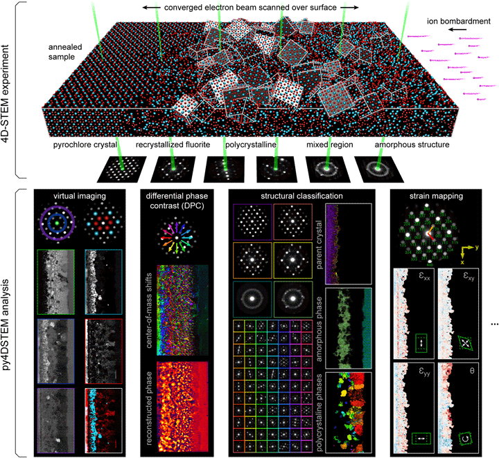
In a four-dimensional STEM (4D-STEM), we replace the standard STEM detectors, which integrate all electrons scattered over a large region, with a pixelated detector that captures the electron flux scattered to each angle in the diffraction plane (Zaluzec, Reference Zaluzec2002; Fundenberger et al., Reference Fundenberger, Morawiec, Bouzy and Lecomte2003; Watanabe & Williams, Reference Watanabe and Williams2007; Lupini et al., Reference Lupini, Chi, Kalinin, Borisevich, Idrobo and Jesse2015; Tate et al., Reference Tate, Purohit, Chamberlain, Nguyen, Hovden, Chang, Deb, Turgut, Heron, Schlom, Ralph, Fuchs, Shanks, Philipp, Muller and Gruner2016; Ophus, Reference Ophus2019). While a typical STEM image, therefore, produces a single number for each position of the electron beam, a 4D-STEM dataset produces a two-dimensional image of diffraction space intensities for each real space beam position. The resulting four-dimensional data hypercube can be collapsed in real space to yield information comparable to more traditional electron diffraction experiments. Alternatively, it can be collapsed in diffraction space to yield a variety of “virtual images,” corresponding to both traditional STEM imaging modes as well as more exotic virtual imaging modalities (Schaffer et al., Reference Schaffer, Gspan, Grogger, Kothleitner and Hofer2008; Tao et al., Reference Tao, Niebieskikwiat, Varela, Luo, Schofield, Zhu, Salamon, Zuo, Pantelides and Pennycook2009; Gammer et al., Reference Gammer, Ozdol, Liebscher and Minor2015; Zhang et al., Reference Zhang, Ning, Busbee, Shen, Kiggins, Hua, Eaves, Davis, Shi, Shao, Zuo, Hong, Chan, Wang, Wang, Sun, Xu, Lui and Braun2017; Hachtel et al., Reference Hachtel, Idrobo and Chi2018). More information still can be extracted by judicious combination of real and reciprocal space. The structure, symmetries, and spacings of Bragg disks can be used to extract spatially resolved maps of crystallinity, grain orientations, and lattice strain (Schwarzer & Sukkau, Reference Schwarzer and Sukkau1998; Usuda et al., Reference Usuda, Numata, Irisawa, Hirashita and Takagi2005; Béché et al., Reference Béché, Rouviere, Clément and Hartmann2009; Caswell et al., Reference Caswell, Ercius, Tate, Ercan, Gruner and Muller2009; Koch et al., Reference Koch, Özdöl and Ishizuka2012; Kobler et al., Reference Kobler, Kashiwar, Hahn and Kübel2013; Pekin et al., Reference Pekin, Gammer, Ciston, Minor and Ophus2017; Hou et al., Reference Hou, Ashling, Collins, Krajnc, Zhou, Longley, Johnstone, Chater, Li, Coulet, Llewellyn, Coudert, Keen, Midgley, Mali, Chen and Bennett2019). Redundant information in overlapping Bragg disks can be leveraged to deconvolve the electron beam shape from the sample structure, yielding the sample potential itself (Chen et al., Reference Chen, Weyland, Ercius, Ciston, Zheng, Fuhrer, D'Alfonso, Allen and Findlay2016; Lazić et al., Reference Lazić, Bosch and Lazar2016; Müller-Caspary et al., Reference Müller-Caspary, Duchamp, Rösner, Migunov, Winkler, Yang, Huth, Ritz, Simson, Ihle, Soltau, Wehling, Dunin-Borkowski, Van Aert and Rosenauer2018). Rings of diffracted intensity, characteristic of amorphous samples, can be used to extract correlation functions describing the short and medium range order and disorder. Indeed, the range of possible quantities of physical interest which can be extracted from a single 4D-STEM experiment is formidable, leading others to use the term “universal detectors” for 4D-STEM capable pixelated cameras (Hachtel et al., Reference Hachtel, Idrobo and Chi2018). Figure 1 shows the experimental geometry of a 4D-STEM experiment, and various measurements performed from the same experimental dataset. For a mathematical discussion of STEM and 4D-STEM image formation, see Appendix A.
Fig. 1. 4D-STEM experimental geometry, and multimodal data analysis with py4DSTEM. An irradiated Gd2Ti2O7 sample contains complex, nanoscale structure, apparent in the distinct electron diffraction patterns across the field of view. From a single 4D-STEM experiment, py4DSTEM enables a range of measurements to be performed in post-processing, including virtual imaging, differential phase contrast, structural classification, strain mapping, and much more. Note that in the DPC subpanel, the final result has been labeled “pseudo-DPC image” to reflect the fact that this image should not be interpreted in terms of the sample potential. Why this is the case, and when such an identification can reasonably be made, is discussed further in the section “Electron phase retrieval.” Additional experimental details can be found in Table 1.
Table 1. Experimental Parameters.

Dose is given here in units of electrons per probe, rather than electrons per Å2. This choice avoids an ambiguity inherent in the latter units, namely: do we consider the area associate with each scan position to be the region illuminated by the probe, or the region constituting a single real space pixel? The former is defined by the probe size, and the latter by the scan step size; both result in meaningful physical quantities, but they may be quite different from one another.
* From Yang et al. (Reference Yang, Rutte, Jones, Simson, Sagawa, Ryll, Huth, Pennycook, Green, Soltau, Kondo, Davis and Nellist2016b).
** Simulated data.
The price paid for the versatility of 4D-STEM is new complexity in both the raw experimental data and in the computational processing required to extract meaningful measurements. Maximizing the impact this new generation of STEM experiments will have on structural characterization research now requires that the computer processing methods which enable the various 4D-STEM characterization modalities are accessible to a broad and diverse segment of the scientific community. Fortunately, a new generation of open-source tools for electron scattering experiments is presently on the rise, such as hyperspy, pyXem, liberTEM, pycroscopy, ncempy, and others (de la Peña et al., Reference de la Peña, Prestat, Fauske, Burdet, Jokubauskas, Nord, Ostasevicius, MacArthur, Sarahan, Johnstone, Taillon, Lähnemann, Migunov, Eljarrat, Caron, Aarholt, Mazzucco, Walls, Slater, Winkler, pquinn-dls, Martineau, Donval, McLeod, Hoglund, Alxneit, Lundeby, Henninen, Zagonel and Garmannslund2019; Nord et al., Reference Nord, Webster, Paton, McVitie, McGrouther, MacLaren and Paterson2019; Johnstone et al., Reference Johnstone, Crout, Laulainen, Høgås, Martineau, Bergh, Smeets, Collins, Morzy, Ånes, Prestat, Doherty, Ostasevicius, Danaie and Tovey2019; Somnath et al., Reference Somnath, Smith, Laanait, Vasudevan and Jesse2019; Clausen et al., Reference Clausen, Weber, Ruzaeva, Migunov, Bahuleyan, Caron, Chandra, Nord, Ophus, Peter, van Schyndel, Shin, Müller-Caspary and Dunin-Borkowski2020).
Here, we present free and open-source software for analysis of 4D-STEM data. The aim of the Python-based project is threefold:
(1) To make 4D-STEM data analysis easy and accessible for everyone;
(2) To facilitate reproducibility, even in cases of complicated or multi-step processing workflows; and
(3) To provide a comprehensive, robust suite of 4D-STEM tools, enabling high-throughput, multimodal analysis in which a single dataset can simultaneously provide many distinct measurements of the sample structure.
For ease and accessibility, py4DSTEM includes a complete application programming interface (API) with associated documentation pages, many fully worked examples in the form of fully commented and interactive Jupyter notebooks. A graphical user interface is under development, and currently supports quick data visualization and some strain mapping functionality. For reproducibility, py4DSTEM defines a set of structured data object types for 4D-STEM data processing, establishes a set of HDF5-based file format conventions for 4D-STEM data, and makes it easy to release, with any publication, the complete and fully transparent code which generates results and figures from raw data. For multimodal, high-throughput analysis, py4DSTEM includes a comprehensive suite of tools for structural analysis in crystalline and amorphous materials, including virtual imaging, phase and orientation mapping, strain mapping, radial distribution analysis, phase contrast imaging, classification, and more. A self-consistent framework allows many or even all of these measurements to be readily performed on a single dataset. The API and sample code for various analysis pipelines are freely available from the py4DSTEM repository.
The organization of this document is as follows: following this introduction, Section “4D-STEM data” discusses the nature of 4D-STEM data, and how data is structured in py4DSTEM. Section “Basic processing” discusses basic processing algorithms which will typically be performed as precursors to the final measurements of interest, including locating Bragg disks, calibration, polar transformations, and classification. Section “Measurements and applications” covers various 4D-STEM measurements that can be performed in py4DSTEM, including virtual imaging, phase mapping, strain mapping in amorphous or crystalline materials, short and medium range order analysis in amorphous materials, and phase retrieval in very thin samples. Conclusions are given in the last section. Throughout, we have aimed to keep discussion qualitative in the main text and have also included mathematical details for the interested reader in a number of appendices, referenced in the relevant sections.
4D-STEM Data
Fundamentally, most 4D-STEM are just many electron diffraction experiments being run sequentially. The nature of the diffraction pattern obtained at each scan position depends on the sample structure and the illumination conditions of the microscope, as illustrated schematically in Figure 1. In crystalline materials and with small-angle illumination, the periodic structure of the sample gives rise to a periodic pattern of disks in the diffraction plane (Carter & Williams, Reference Carter and Williams2016). A bright disk appears wherever the Bragg condition is met, with the disk positions reflecting a slice through the reciprocal lattice of the crystal. In amorphous materials, concentric rings of diffuse intensity appear centered about the optic axis (Egami & Billinge, Reference Egami and Billinge2003). The radii of these rings reflect the characteristic spacings of the atoms in the sample and can, therefore, be used to extract statistical measures of structure, such as the radial distribution function. In analyzing crystalline materials, the crux of the analysis will generally be measuring the Bragg angles in each diffraction pattern, by determining the positions of all the Bragg disks. In analyzing amorphous materials, analysis will generally revolve around radial integration of the diffraction patterns. In samples containing both crystalline and amorphous regions, both types of analysis can be performed in concert.
Experimental Conditions
A complete discussion of the many experimental conditions to be aware of in devising a given 4D-STEM experiment is beyond our scope, however, one parameter stands apart in its centrality to both acquiring and understanding 4D-STEM data: the convergence semi-angle, α. When examining a diffraction pattern, α corresponds to the radius of the bright-field disk in the diffraction plane, and therefore also the radius of each refracted Bragg disk in a crystalline sample. In real space, the probe size is inversely related to α; larger convergence angles correspond to finer probes; and overlapping disks are required to generate sub-lattice-sized probes and, therefore, allow atomic resolution imaging (Kirkland, Reference Kirkland2010). In extracting a strain map, for example, nonoverlapping disks are important, both to facilitate the detection of the disk positions, and also because strain is a physical quantity only defined on length scales equal to or larger than single unit cells.Footnote 1 For a ptychographic reconstruction of the atomic potentials of very thin materials, overlapped disks are essential, as they provide the redundant information required to extract the phase of the electron wavefunction and the sample electrostatic potential (Hegerl & Hoppe, Reference Hegerl and Hoppe1970). For analysis of amorphous materials, measuring radial distribution functions requires nearly parallel illumination (a small semi-convergence angle), while measurements of medium range order in fluctuation electron microscopy experiments will often vary the probe semi-angle to probe different sizes of atomic clusters (Rodenburg, Reference Rodenburg1999; Mu et al., Reference Mu, Wang, Feng and Kübel2016). In general, the convergence angle should be selected carefully in light of the particular requirements of the experiment.
The convergence semi-angle, accelerating voltage, and associated figures for all 4D-STEM data herein are in Table 1.
Multimodal Analysis: One Dataset, Many Measurements
A major advantage of 4D-STEM is the ability to perform a single experiment from which many distinctly meaningful structural measurements can be made. We take as our guiding example the Gd2Ti2O7 (GTO) crystal shown in Figure 1. A pyrochlore-structured GTO single crystal was first bombarded with ions, creating an amorphized layer. The sample was then annealed, creating both a layer of recrystallization on the parent lattice as well as a band of smaller crystallites embedded in an amorphous matrix. Each of these regions is clearly visible in the diffraction patterns associated with various beam positions of the 4D-STEM scan.
A selection of the types of measurements that can be performed from this dataset are shown in the figure. They include virtual imaging spanning bright-field images, annular dark-field images, and dark-field images of individual or multiple Bragg reflections (see Section “Virtual imaging”); differential phase contrast imaging, whereby shifts in the center of mass of the beam are used to back out the sample structure; strain mapping, showing the local deformations of the atomic lattice (see Section “Crystalline strain mapping”); and structural classification, where regions of distinct structure are identified and segmented (see Sections “Classification” and “Structural phase mapping”). With py4DSTEM, these analyses and more can all be applied to a dataset within a single, unified framework.
Data Structures
Data in py4DSTEM are structured in five different types, broadly distinguished by their dimensionality, shown in Figure 2. In-program, these are implemented as the following Python classes: DataCube, DiffractionSlice, RealSlice, PointList, and PointListArray. DataCube instances contain a 4D data array corresponding to the complete 4D-STEM dataset. DiffractionSlice and RealSlice instances contain one or more 2D arrays with shapes corresponding to that of diffraction space (i.e., the detector shape) or of real space (i.e., the raster scan shape), respectively. A DiffractionSlice might contain a single diffraction pattern, an image of the probe over vacuum, or the average background noise on the detector. A RealSlice might contain a virtual image, a Boolean mask indicating scan positions to be included or excluded in an analysis routine, or the x- and y-components of a lattice vector calculated at each scan position. This last example describes a RealSlice of depth 2, that is, the data contained in the RealSlice class instance are a 3D array consisting of a stack of two 2D arrays in the shape of real space (x and y of the lattice vector); in general, DiffractionSlice and RealSlice objects can have arbitrary depth. The PointList class is flexible, containing a set of points of arbitrary length in an arbitrary number of dimensions, from simple 1D data to arbitrarily high-dimensional data. On instantiation of a PointList, a set of coordinates must be specified—for example, to specify the positions and intensities of the Bragg disk positions detected in a single diffraction pattern (“qx,” “qy,” “intensity”) might be used. Points may then be added or removed from the PointList, for example, as Bragg disks are detected and then thresholded. Data in PointLists can be easily extracted or sorted by chosen coordinates. PointListArray instances are 2D arrays of PointLists, organized in memory to facilitate quick access of the PointList corresponding to a single array element, and are useful when storing a PointList for each scan position. The DataCube class contains a 4D dataset. Interfaces are provided to load an entire 4D datacube directly into memory, or to create a memory map to the dataset, enabling analysis of datasets larger than the system's memory. All these datastructure classes inherit from a parent class called DataObject which facilitates basic searching, storing, and saving functionality for all data generated by py4DSTEM, as well as linking to any relevant metadata.

Fig. 2. py4DSTEM data structures. Data are saved as one of five classes of dataobjects—DataCube, DiffractionSlice, RealSlice, PointList, and PointListArray objects.
File Structure
py4DSTEM saves data in the Hierarchical Data Format or HDF5 format, described on the HDF5 website (The HDF Group, 2020). A description of the flavor of HDF5 used in py4DSTEM, which we refer to as “electron microscopy datasets” or EMD files, is available on the EMD website. Each HDF5/EMD file generated by py4DSTEM has a top-level group containing all data, allowing for the possibility of nesting many py4DSTEM files in a single, larger file, and version tags to allow for backwards compatibility. Within the top-level group, a py4DSTEM file contains three high-level groups: data, metadata, and log. The data group typically contains five subgroups corresponding to the five datastructures discussed in the previous section, and each subgroup, in turn, contains any number of nested subgroups, each storing the contents of a single corresponding dataobject, including its raw data and any relevant metadata (e.g., the length of a PointList, the dimensions of a DiffractionSlice, etc.). This structure makes it possible to bundle all elements of one or more data processing pipelines pertaining to a single raw dataset in a single location and simplifies reuse between measurements of any shared datastructures.
Loading data necessarily varies based on the input file type. For its native HDF5 files, py4DSTEM supports scanning the contents of a file before pulling anything into memory, so the entirety of large files need not be loaded if only some subset of smaller dataobjects are required. For very large datasets, the memory mapping of datacubes is supported, whereby the contents of a loaded datacube object are left in nonvolatile storage, and individual diffraction patterns are pulled into RAM only as they are accessed, enabling analysis of datasets that are larger than available system RAM. For non-native files, py4DSTEM makes use of the i/o module of openNCEM to handle various filetypes produced by electron microscopy experiments. Binning during loading is supported for some file formats.
For non-native files, many of the file types used in electron microscopy are proprietary and the contents are not publicly described, which hinders scientific progress within electron microscopy. py4DSTEM, therefore, relies on the i/o components of two other open-source projects, hyperspy and openNCEM.
The metadata group contains six subgroups: microscope, sample, user, calibration, comments, and original. The microscope group contains information related to the microscope setup and acquisition parameters, such as the accelerating voltage of the beam, the camera length, the convergence angle, and so forth. The sample group stores information such as the material imaged, synthesis information, and any sample preparation. The user group is for information related to the scientist or scientists who obtained the data, including names, institutions, and contact information. The calibration group contains the pixel sizes (in real and diffraction space), as well as any additional calibration information such as rotational offsets, diffraction shifts, and elliptical distortions, which will be discussed in more detail in the section “Calibration.” The comments group is for any miscellaneous comments. The original group contains any raw metadata scraped from the original data file.
More details about the program structure, interface, implementation, and usage, including its data handling, modules, the 4D-STEM HDF5 file structure, logging, and metadata handling is available in the py4DSTEM documentation, or in the py4DSTEM repository.
Basic Processing
In this section, we discuss the basic processing required for most datasets, namely: preprocessing in the section “Preprocessing,” Bragg disk detection (for crystalline samples) in the section “Bragg disk detection,” calibration in the section “Calibration,” polar transformations (for amorphous samples) in the section “Polar transformation,” and classification in the section “Classification”. These processing steps are basic in the sense of underpinning all subsequent analyses, rather than in the sense of simplicity; these methods are not aimed at producing a final measurement or plot, but rather are the necessary preparatory work to ensure such ultimate measurements are possible, and are optimally accurate. Measurements and applications are addressed in the next section.
Preprocessing
This section discusses several preprocessing steps that may be performed on a 4D-STEM dataset. None of these steps are universally required; however, care in preprocessing can significantly speed up subsequent processing and lead to higher accuracy and precision in final analyses. Preprocessing should, in general, be tailored to the individual dataset, as the dominant forms of noise will typically depend on the camera used, as well as acquisition parameters; here, we focus on a single example of the preprocessing performed to remove deleterious artifacts present in the GTO dataset, acquired on a Gatan K2 camera. This preprocessing was applied before all other analysis preformed on this dataset (see Table 1 for relevant figures).
Figure 3a shows a position-averaged diffraction pattern from the GTO dataset. Vertical streaks resulting from gain differences in the columns of detector pixels are apparent in the image. This is due to the gain and dark reference images on the camera being imperfect; here, we demonstrate correcting this imperfection in post-processing. There are also a handful of individual saturated pixels, likely resulting from stray X-rays. Hot pixels were identified and zeroed using median filtering. The background was determined by identifying edges of the detector which were beyond the high-angle annular dark-field (HAADF) detector and should ideally have no counts, then using this region (shown in yellow) over many diffraction patterns to calculate the average background streaking. This assumes that the streaking is constant across the images. Alternatively, one or many dark reference images can be recorded directly. The new average diffraction image after background subtraction is shown in Figure 3b.

Fig. 3. Preprocessing. (a) A position averaged diffraction pattern of raw 4D-STEM data. (b) The same position averaged diffraction pattern after subtracting a background determined from the yellow regions in (a). As the focus here is preprocessing, both (a) and (b) have been scaled logarithmically and their histograms clipped identically in both images on the high end to enable visualization of background noise and streaking; this also results in apparent saturation of the central beam in this visualization. There is no saturation in the raw dataset. (c,d) The initial step of an electron counting procedure, in which minimum and maximum thresholds (black and red dashed lines, respectively) of the pixel intensities are used to rule out background pixels and X-ray strikes. (e,f) Binning and cropping. Scale is arbitrary in these images, which are shown for bin/crop demonstration purposes.
In 4D-STEM data with a sufficiently low electron dose and a suitably low noise direct electron detector, it is possible to detect individual electron strike events. Electron counting, that is, determining and recording the diffraction space positions of each electron incident on the detector, is beneficial for both noise reduction and data compression. Many direct electron detectors automatically perform the electron counting at the hardware level. However, most detectors with a reasonably small point spread function and good quantum efficiency can be used as a counting detector, provided that the electron fluence is low enough. We have, therefore, included an electron counting routine in py4DSTEM, which estimates the location of individual electron strikes. For more information on the benefits of electron counting, we refer the readers to Li et al. (Reference Li, Zheng, Egami, Agard and Cheng2013).
Our electron counting implementation begins by first calculating a dark reference for the detector. A histogram of pixel intensity values is then generated from a random sampling of detector frames and is used to calculate an upper intensity threshold (for excluding X-ray strikes) and a lower intensity threshold (for excluding the background). In Figure 3, the histograms in panels (c,d) correspond to the low-dose dataset shown in panels (e,f). These diffraction patterns were recorded by placing an “amplitude plate” aperture in a condenser aperture, as described in Zeltmann et al. (Reference Zeltmann, Müller, Bustillo, Savitzky, Hughes, Minor and Ophus2020). Looping through each scan position, the dark reference is subtracted and the thresholds are applied to each detector frame, and the local maxima of the resulting image are identified. These local maxima are considered electron strike events. Optionally, their positions can be refined to subpixel precision. Counted data are stored as a PointListArray, that is, for each scan position, we save a list of detector positions of electron strike events. If data is required in the form of 2D images during subsequent analysis, these can then be generated directly from the associated PointList. The compression level achieved will vary with the individual dataset and depends strongly on dose. Lower dose data will contain electron strike events in a lower the fraction of pixels, and thus allow for greater compression; see also Nord et al. (Reference Nord, Webster, Paton, McVitie, McGrouther, MacLaren and Paterson2020) and Ercius et al. (Reference Ercius, Johnson, Brown, Pelz, Hsu, Draney, Fong, Goldschmidt, Joseph, Lee, Ciston, Ophus, Scott, Selvarajan, Paul, Skinner, Hanwell, Harris, Avery, Stezelberger, Tindall, Ramesh, Minor and Denes2020). For the dataset shown in the figure, electron counting compresses the data by a factor of ~6,000.
The most basic preprocessing functions include reshaping, binning, and cropping data. Binning and cropping can be performed in either real or diffraction space and allow large datasets to be reduced to more manageable sizes. For selected file formats, py4DSTEM also supports data binning on import. Figures 3e and 3f show an electron beam which has been shaped using a structured condenser aperture; from panels (e) to (f), this data has been cropped and binned by a factor of three. Reshaping the data may be necessary in some cases, for instance, some file formats do not contain complete information about the real space scan shape, and thus can be initially loaded as 3D arrays (with the two real space dimensions collapsed into one) before being correctly reshaped into 4D arrays.
Bragg Disk Detection
For crystalline or semi-crystalline data, analysis generally begins by identifying the locations of all the Bragg disk reflections in each diffraction pattern, which correspond to the reciprocal lattice points of the crystal. In py4DSTEM, we find the Bragg disk positions in two steps: first, we extract a 2D image of the probe pattern over vacuum in diffraction space to use as a template. This can be thought of as the image of the aperture in diffraction space. We then find the Bragg disks by determining all the positions in each diffraction pattern that match the structure of this template (Pekin et al., Reference Pekin, Gammer, Ciston, Minor and Ophus2017). The Bragg disk detection procedure is illustrated in Figure 4 for the GTO dataset.

Fig. 4. Bragg disk detection in GTO. (a) The vacuum probe. The bright rim visible at the disk edge is the result of slight defocus, resulting in Fresnel diffraction at the sharp edges. (b) A virtual bright-field image. (c) Disk detection is accomplished by the cross-correlation of the probe template with each diffraction pattern, illustrated schematically here. (d–g) Diffraction patterns corresponding to the four scan positions indicated in (b). (h–k) The detected Bragg peaks for these four diffraction patterns. The size of each circle indicates the cross-correlation intensity, a rough approximation for disk intensity.
py4DSTEM includes three methods for generating vacuum probes. Ideally, we use an image or averaged image stack of the probe over vacuum. Alternatively, if an experimental 4D-STEM scan contains a vacuum region, or a region with only very thin material (e.g., amorphous carbon support), this thin region can be used to generate a vacuum probe. In this case, the probes from each vacuum scan position should be aligned, to correct the translation of the diffraction patterns as the beam is scanned, and then averaged. Alignment is performed by cross-correlating pairs of vacuum template images, determining their relative offset, then shifting the second image to align with the first. Finally, if neither of these options are possible, a synthetic probe can be generated—see Appendix C.
Once a vacuum probe has been obtained, two additional processing steps are applied, with the purpose of generating a kernel for cross-correlative template matching with the individual diffraction patterns. First, the central diffraction disk is located and its center is shifted to the origin. Without this step, all measurements will have an offset, leading to incorrect results. Second, a Gaussian wider than the probe is subtracted, leading to a region of negative intensity surrounding the probe itself, such that the total integrated intensity of the kernel is zero. This has two advantages. First, it ensures that the cross-correlation of noisy data is, on average, zero where there are no Bragg disks. Second, the negative kernel intensity penalizes the cross-correlation values where a Bragg disk and a template are slightly misaligned, enhancing the detectability of correlation maxima where disk/template alignment is perfect. The method of subtraction of a Gaussian reported here is found to be a useful heuristic and has a similar effect to other edge filtering methods such as Laplacian of Gaussian filtering or pre-filtering with a Sobel filter; other similar approaches are described elsewhere (Williamson et al., Reference Williamson, van Dooren and Flanagan2015; Grieb et al., Reference Grieb, Krause, Mahr, Zillmann, Müller-Caspary, Schowalter and Rosenauer2017, Reference Grieb, Krause, Schowalter, Zillmann, Sellin, Müller-Caspary, Mahr, Mehrtens, Bimberg and Rosenauer2018; Pekin et al., Reference Pekin, Gammer, Ciston, Minor and Ophus2017; Mahr et al., Reference Mahr, Müller-Caspary, Ritz, Simson, Grieb, Schowalter, Krause, Lackmann, Soltau, Wittstock and Rosenauer2019; Padgett et al., Reference Padgett, Holtz, Cueva, Langenberg, Schlom and Muller2019). Adding structure to the electron probes using an amplitude mask in the condenser aperture has also been shown to significantly enhance the precision of Bragg disk detection (Zeltmann et al., Reference Zeltmann, Müller, Bustillo, Savitzky, Hughes, Minor and Ophus2020).
The Bragg disks are located by calculating the cross-correlation of the probe kernel with each diffraction pattern, and then locating the correlation maxima. The disk positions can be located with subpixel precision via local Fourier upsampling in the region about each maximum (Soummer et al., Reference Soummer, Pueyo, Sivaramakrishnan and Vanderbei2007; Guizar-Sicairos et al., Reference Guizar-Sicairos, Thurman and Fienup2008). The correlations are here performed on the raw (unnormalized) data, which is beneficial as it means that the resulting cross-correlation intensity of each Bragg disk will roughly reflect its scattering intensity. This also enable global thresholding across the dataset. In contrast, normalizing the data first may be useful in the case of samples containing different regions which give rise to significantly different diffracted intensities. py4DSTEM allows for standard cross-correlations, as well as phase or hybrid correlations, to be performed at this stage; see Appendix B for detailed discussion.
The detected Bragg disks in each diffraction pattern are stored in a PointList instance with three coordinates specifying the disk position in the diffraction plane and its cross-correlation intensity (q x, q y, I). The Bragg disks from the complete datacube are stored in a PointListArray instance, with one such PointList for each scan position. For many analyses, such as strain or orientation mapping, all subsequent computation can be performed on this PointListArray alone, as it contains the most crucial scattering information. The data compression here is significant, as only three numbers are now required to store each Bragg disk. For a datacube consisting of 512 × 512 pixel diffraction patterns with a bit depth of 16, 20 detected disks in an average diffraction pattern, and using 64-bit floating point numbers for the disk coordinates, this scheme compresses the data by a factor of approximately 1,000.
Once the Bragg disks have been detected, all peaks from all scan positions may be collapsed into a single image in the shape of the diffraction plane. The resulting object is roughly interpretable as a position averaged probability distribution of reciprocal lattice points and is defined carefully in Appendix D. Figure 5 shows an example using the GTO dataset. We refer to this object as a Bragg vector map (BVM). Figure 5a shows the BVM of the complete GTO 4D-STEM scan, while Figures 5c–5f show the BVMs generated from subsets of the scan region indicated in the virtual image shown in Figure 5b. The BVM of the single-crystal region in Figure 5c shows sharp reciprocal lattice peaks of the orthorhombic crystal in the  $\langle 01\bar {1}\rangle$ projection. The BVM of Figure 5d also contains sharp peaks, now oriented isotropically about the origin, indicating many small, randomly oriented crystal grains. Figure 5d also shows a faint ring resulting from amorphous scattering in this mixed cystalline/amorphous region. In principle, this ring could also result from small, randomly oriented crystallites; in this case, comparison with the raw data indicates these result from nonzero cross-correlation with the amorphous signal. Note that ideally the BVM would be insensitive to amorphous scattering because it should only contain counts where Bragg scattering occurs, however, false-positive Bragg disk detection can occur in the amorphous halo, resulting the ring here as well as in Figure 5f. False positives are also apparent near the aperture edge in Figure 5a. Figure 5e shows little amorphous signal, sharp peaks indicating crystal scattering, and fewer peaks than in Figure 5d, suggesting that this layer of the sample may contain fewer, larger crystallites. Figure 5f shows little or no crystalline signal, suggesting a purely amorphous layer. Phase mapping, found in the section “Structural phase mapping,” confirms these hypotheses about the sample structure. In general, some number of false positives are to be expected, with their exact numbers and origins depending on the data and on how the cross-correlation is performed. Note that the number of false positive in, for instance, Figure 5f is relatively small but is visually enhanced here by the choice of logarithmic scaling. Raising the minimum intensity of cross-correlation maxima to identify with a Bragg peak can help minimize false positive. Using pure cross-correlations, rather than phase or hybrid correlations which are more sensitive to noise (see Appendix B) can also help, as can alternate template matching approaches using pre-filtering or structured probes, as discussed previously.

Fig. 5. Bragg vector maps (BVMs) of GTO. (a) The BVM from the complete dataset. (b) Virtual bright-field image with boxes indicating four regions of interest. (d–f) BVMs generated from the four corresponding regions shown in (b). All these BVMs are shown in a single logarithmic scale.
BVMs are a useful tool in 4D-STEM data processing. In py4DSTEM, they are used in processing pipelines including calibration (see Fig. 6), classification (see Fig. 8), strain mapping (see Fig. 11), and others.
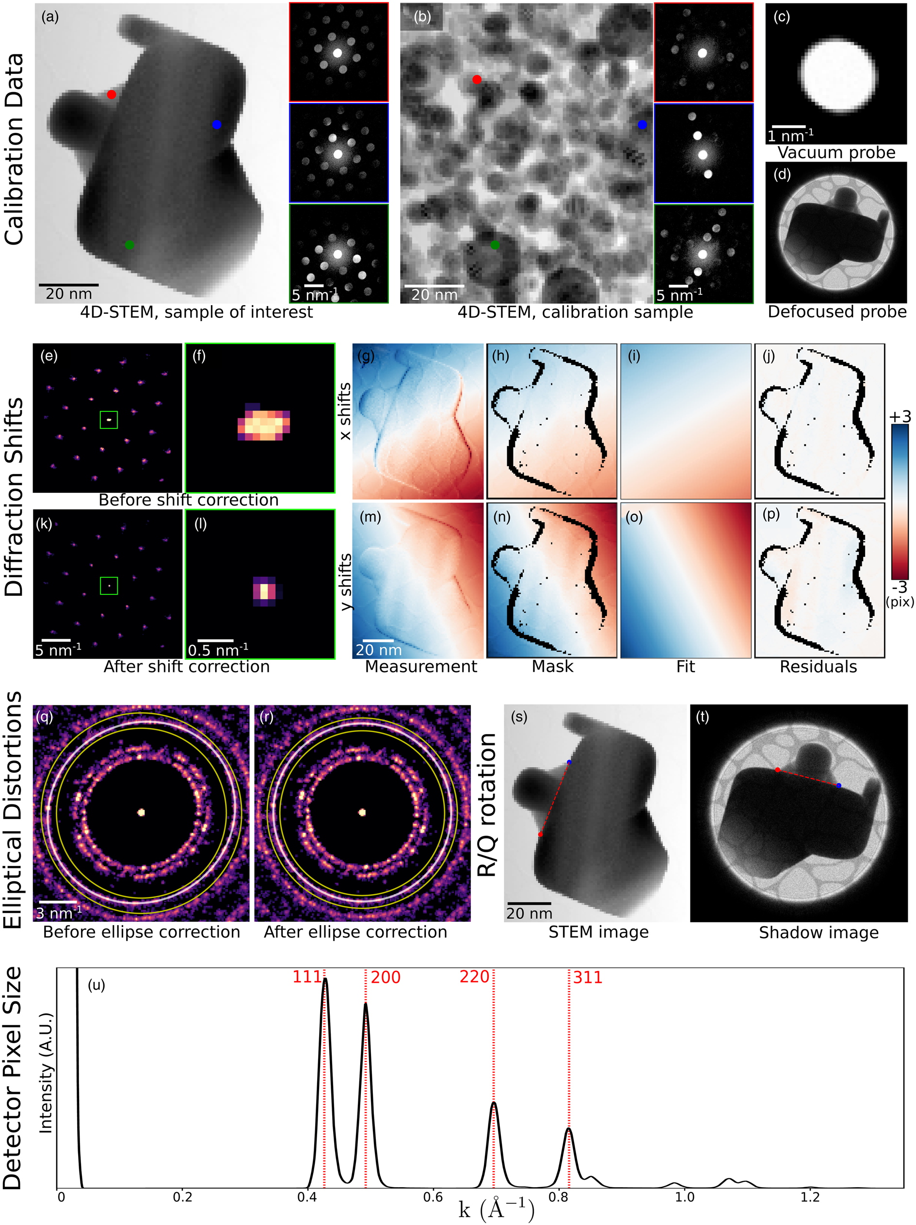
Fig. 6. Calibration. (a–d) The recommended data to collect in order to fully calibrate a 4D-STEM dataset. Data shown here have been simulated. (a) A 4D-STEM dataset of a sample of interest, here a strained, single-crystal gold nanoparticle. (b) A 4D-STEM dataset of a standard calibration sample, here a distribution of gold nanoparticles. In both (a) and (b), a virtual bright-field image and three selected diffraction patterns of the 4D-STEM datasets are shown. (c) An image or 3D image stack of the probe over vacuum. Here, simulated tilt in the projector and condenser systems yields a slightly elliptical probe shape. (d) An image of the probe over the sample and defocused until a shadow image is visible. (e–u) A complete set of 4D-STEM calibrations. (e–p) Measurement and correction of translations of the diffraction patterns with the beam raster. (q–r) Measurement and correction of elliptical distortions. Shown here are the BVM before and after correction. (s,t) Measurement of the rotational offset of the electron beam between the real and diffraction planes. (u) Measurement of the detector pixel size.
Calibration
Calibration is the single most important step of any quantitatively meaningful 4D-STEM data analysis, as all subsequent measurements hinge on the accuracy of the calibration. In 4D-STEM, a number of calibrations are typically desirable. These include correcting shifts of the diffraction pattern from the raster of the beam, correcting elliptical distortions of the diffraction patterns, calibrating the rotational offset between real and diffraction space, and calibrating the pixel sizes. The type of calibrations required will generally depend on the sample being imaged, the measurements being made, and the required precision.
The data required to perform calibrations are similarly contingent and depend on the structure of the sample, as well as which calibrations need to be performed. An image or a 3D stack of images of the STEM probe over vacuum should always be acquired and is important for analyses including Bragg disk detection, calibration of the convergence semi-angle, and deconvolution of the probe. Scanning a standard calibration sample of known structure at the beginning or end of a microscope session is highly recommended and will typically ensure the most accurate calibration of pixel sizes. Using a polycrystalline standard calibration sample is also highly recommended, to facilitate calibration of inevitable elliptical stretching of the diffraction patterns due to imperfect optics and alignments (Mahr et al., Reference Mahr, Müller-Caspary, Ritz, Simson, Grieb, Schowalter, Krause, Lackmann, Soltau, Wittstock and Rosenauer2019). Obtaining an image of the probe, positioned over the sample and then highly defocused to create a shadow image in the diffraction plane, is the recommended data for calibrating the real/diffraction space rotational offset. In some cases, it is possible to obtain the necessary calibrations directly from the experimental 4D-STEM scan; however, the viability of this approach is not guaranteed and is especially dubious for samples of unknown structure.
Figure 6 shows the complete calibration of a simulated dataset (Ophus & Savitzky, Reference Ophus and Savitzky2019). We simulated two 4D-STEM datasets: one scan of the sample under inquiry and one scan of a calibration sample. For the inquiry dataset, we simulated a large single-crystalline gold nanoparticle under differing amounts of strain in various areas of the sample (Fig. 6a). For the calibration dataset, we simulated gold small nanoparticles oriented randomly on a thin support (Fig. 6b). We additionally simulated an image of the STEM probe in the diffraction plane (Fig. 6c) and an image of the probe after defocusing to form a shadow image (Fig. 6d). Simulations were performed using the PRISM algorithm (Ophus, Reference Ophus2017; Pryor et al., Reference Pryor, Ophus and Miao2017), using a 300 kV beam, 0.2 Å pixels, a 10 Å slice thickness, a 2 mrad convergence semi-angle, a 10 Å probe step size, and a PRISM interpolation factor of 12 in x and y. We post-processed the data by applying a large Gaussian centered on the probe to simulate an inelastic background, and a beam shift and elliptic distortion to all patterns. We used Poisson statistics to calculate images with 105 electrons per pattern.
Diffraction shifts—overall translation of the diffraction patterns resulting from the scanning of the electron beam—yield apparent shifts of the position optic axis from one diffraction pattern to the next (Craven & Buggy, Reference Craven and Buggy1981). The size of the diffraction shifts depends on the real space field-of-view of the scan, on the camera length, and on the particular instrument used; generally speaking, we recommend measuring diffraction shifts in scans larger than a few tens of nanometers, and then applying corrections if deemed necessary. In py4DSTEM, this calibration is performed by identifying the unscattered beam at each scan position and measuring the shifts in its position. These shifts are then fit to a plane or low-order polynomial, which can be used to correct the diffraction shifts. For correcting the shifts, it is possible to shift each diffraction pattern by the measured amount to generate a new, corrected datacube; however, this is slow, resource intensive and often unnecessary. Instead, it is often possible to simply use the measured shift values to set the origin of coordinates in any subsequent measurements made on individual diffraction patterns. Figures 6e–6p show BVMs before (e,f) and after (k,l) diffraction shift corrections have been applied to the measured Bragg peak positions. The zoomed in images centered on the central peak (Figs. 6f, 6l) illustrate that the blurred peak of Figure 6f collapses to a sharp peak in Figure 6l after shift correction. In Figures 6g–6p, we show the initial measurement of shifts of the central disk, a masking step to ignore some subset of data points, a smooth fit to the data, and the residuals, which are all much less than a single pixel.
Elliptical distortions, in which circular features about the optic axis are stretched into ellipses, are generally experimentally unavoidable (Mahr et al., Reference Mahr, Müller-Caspary, Ritz, Simson, Grieb, Schowalter, Krause, Lackmann, Soltau, Wittstock and Rosenauer2019). These result from imperfect alignments, including off-axis illumination on the probe-forming condenser aperture, stigmation in the post-specimen optics, and finite tilt of the detector plane relative to the plane normal to the optic axis. Even in a well-aligned system, these distortions may be significant and are, therefore, important to correct in many quantitatively sensitive experiments. In py4DSTEM, elliptical distortions can be measured by fitting an elliptical function to data within some specified annular region, as shown in Figures 6q and 6r. The functional forms of the fits are discussed in more detail in Appendix E. With elliptical fits in hand, the elliptical distortions can be corrected. For crystalline data in which the Bragg peaks have been measured and subsequent analysis will be performed on the measured peak positions only, correction may be accomplished by shifting the peak positions while leaving the raw data untouched. Figure 6r shows a BVM after such correction has been performed. An alternate approach to elliptical correction is to take a polar-elliptical transform, effectively re-sampling the data into a coordinate system which shares the data's ellipticity. This latter approach is frequently useful in analysis of amorphous datasets and is discussed further in the section “Polar transformation.” Note that higher-order elliptical distortions may also be present in diffraction data. At the time of writing these are not corrected, however, the modular nature of the package makes adding these additional calibrations simpler.
In general, there is some angle of rotation between the electron beam in the sample plane and in the detector plane. Thus, in order to correctly map orientations measured in the diffraction plane into real space, it is necessary to measure and account for this rotational offset. The simplest and most robust way to measure the offset is to compare a STEM image to an overfocused probe shadow image. Any STEM image will suffice, provided that the same features are visible in the STEM and shadow images, and in Figure 6, the bright-field virtual image is used. Note that if a shadow image is formed with an underfocused probe instead, the image orientation will be flipped. Two identical points in each of the two images are identified in Figures 6s and 6t and are then used to calculate the rotational offset. If a shadow image has not been obtained, other methods to determine the rotational offset are possible; however, these methods will necessarily be less robust. Two additional techniques for rotational calibration are provided in py4DSTEM, both based on the principles of differential phase contrast imaging. As a result, these methods tend to work well when the assumptions of differential phase contrast hold. They are discussed further, along with the relevant caveats, in the section “Differential phase contrast.”
The calibration of the diffraction space pixel size minimally requires measuring a single diffraction vector with a known spacing. More accurate measurement is possible by fitting to several known spacings. Figure 6u shows a radial integral (see Section “Polar transformation”) of the elliptically corrected BVM shown in Figure 6r. By indexing the peaks observed and using the known lattice spacing of gold, we use the measured peak positions to calculate the detector pixel size. The horizontal axis of these plots can then be written in physical units of Å−1.
Ideally, the real space pixel size is determined by the distance and the electron probe is rastered by the scan coils between detector frames. It is, therefore, equivalent to the size calibration of the instrument's STEM scan. For this reason, processing tools for re-calibration of the real space pixel size are not provided. However, should such calibration be desired, it is straightforward to edit the py4DSTEM metadata based on independent measurement of the real space pixel sizes. When specimen drift leads to large deviations of the pixel size and scan direction angles, further pixel size measurements and drift correction may be required (Sang & LeBeau, Reference Sang and LeBeau2014; Ophus et al., Reference Ophus, Ciston and Nelson2016a; Savitzky et al., Reference Savitzky, El Baggari, Clement, Waite, Goodge, Baek, Sheckelton, Pasco, Nair, Schreiber, Hoffman, Admasu, Kim, Cheong, Bhattacharya, Schlom, McQueen, Hovden and Kourkoutis2018; Wang et al., Reference Wang, Suyolcu, Salzberger, Hahn, Srot, Sigle and van Aken2018).
Polar Transformation
Transformation from Cartesian to polar coordinates is an important operation in many 4D-STEM analyses, especially of amorphous data. Sections “Radial distribution functions” and “Fluctuation electron microscopy” discuss two examples, fluctuation electron microscopy and radial distribution function analysis. Polar-elliptical transformations are useful for correcting elliptical distortions, as discussed in the section “Calibration.” This also enables the calculation of elliptically corrected radial integrals.
Figure 7 shows the transformation of the BVM of the simulated calibration sample of gold nanoparticles described in the section “Calibration.” Both a polar (Figs. 7a, 7c) and polar-elliptical (Figs. 7b, 7d) transformation have been performed, in the latter case using elliptical parameters fit from the image. In the polar case, we see that just as the circular coordinate axes poorly align with the data in Figure 7a, so too do the rings turn into vertical sinusoids in Figure 7c. In contrast, in Figure 7b, the axes and data are well aligned, and in Figure 7d, the rings turn into vertical lines rather than sine curves.
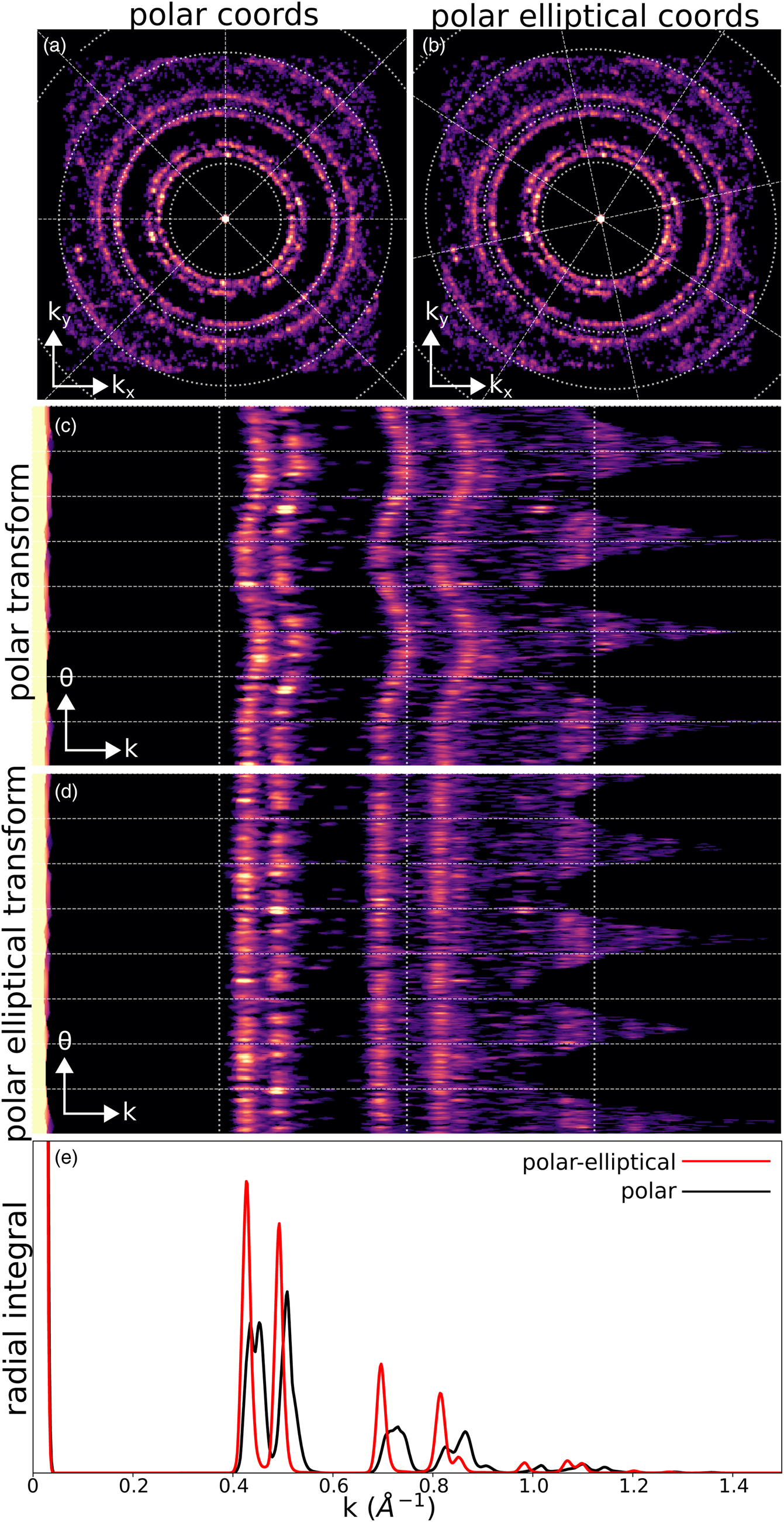
Fig. 7. Polar and polar-elliptical transforms. (a) Bragg vector map of the simulated gold nanoparticle calibration dataset, overlaid with a polar coordinate grid. (b) Identical data to (a), but overlaid with a polar-elliptical grid calibrated to this data. (c) The polar transform corresponding to (a). Note that the rings have been mapped to sinusoids, due to elliptical distortions. (d) The polar-elliptical transform corresponding to (b). The rings now map to lines, indicating that the elliptical calibration is correct. (e) Radial integrals calculated from the polar (black) and polar-elliptical (red) transforms.
The radial integration of a single or averaged diffraction pattern is an important operation, providing higher signal-to-noise (SNR) information about electron scattering at each spatial frequency, at the expense of losing any orientation information. The polar-elliptical transform makes elliptically corrected radial integration easy—just sum along the angular axis of the transformed data. Figure 7e shows an example, with the radial integral calculated from the calibrated polar-elliptical transform in red and the radial integral from the simple polar transform in black. Note that the simple radial integral broadens peaks and, in the case of the first peak, splits a single peak into two apparent, but spurious, peaks.
Classification
In the context of 4D-STEM, classification refers to assigning one or more integer values to each scan position, which identify this position with associated classes. Ideally, each class corresponds to a type of diffraction pattern, or to structurally meaningful features or motifs, such that a scan position will be included in a given class if and only if its diffraction pattern contains these features. Virtual imaging, and thoughtful combination of virtual images and colormaps, is often the easiest way to visually differentiate distinct structural regions and can be a powerful tool for microanalysis (Tao et al., Reference Tao, Niebieskikwiat, Varela, Luo, Schofield, Zhu, Salamon, Zuo, Pantelides and Pennycook2009; Gammer et al., Reference Gammer, Ozdol, Liebscher and Minor2015; Zhang et al., Reference Zhang, Ning, Busbee, Shen, Kiggins, Hua, Eaves, Davis, Shi, Shao, Zuo, Hong, Chan, Wang, Wang, Sun, Xu, Lui and Braun2017; Shukla et al., Reference Shukla, Ramasse, Ophus, Kepaptsoglou, Hage, Gammer, Bowling, Gallegos and Venkatachalam2018). By identifying each pixel with discrete class types, classification goes a step further, facilitating subsequent analyses as well as enabling the generation and identification of class diffraction patterns (Brunetti et al., Reference Brunetti, Robert, Bayle-Guillemaud, Rouviere, Rauch, Martin, Colin, Bertin and Cayron2011; Gallagher-Jones et al., Reference Gallagher-Jones, Ophus, Bustillo, Boyer, Panova, Glynn, Zee, Ciston, Mancia, Minor and Rodriguez2019).
Figure 8 shows a simple classification example. A 4D-STEM scan was taken of a medium entropy alloy containing a twin boundary, which is about three quarters of the way up the virtual image in Figure 8a. Figures 8b–8d show average diffraction patterns, generated by averaging 100 individual patterns, from the regions shown with red, green, and blue squares in Figure 8a. Inspection reveals that the reciprocal lattice in Figure 8b is twinned with respect to that of Figures 8c and 8d. This dataset is, therefore, an excellent testbed for a classification algorithm because the correct answer is immediately apparent: each diffraction pattern in this dataset should be assigned to one of two classes, according to the side of the twin boundary where it falls.

Fig. 8. A 4D-STEM classification algorithm. (a) Virtual bright-field image of a 4D-STEM dataset of a twin boundary, with a 60 mrad camera angle. (b–d) Averages of 100 diffraction patterns each from the regions shown in (a). (e) The Bragg vector map. (f) BVM maxima have been located, labeled, and used to segment the diffraction plane. (g,h) The segmentation in (f) is used to label the Bragg peaks in each diffraction pattern. (j) Co-occurrence of Bragg peaks is used as a criterion to assign scan positions to classes, resulting in a classification which clearly identifies the twin boundary.
The algorithm proceeds as follows. First, all Bragg disks are located, as described in the section “Bragg disk detection.” Next, the BVM is calculated, after any relevant calibrations such as diffraction shift correction have been performed—see Figure 8e. The N maxima of the BVM are then located. A Voronoi tesselation of the diffraction plane is constructed using these maxima as the initial points, which carves the diffraction plane into a set of N regions, each of which is defined as the set of all points closest to one BVM maximum (Barber et al., Reference Barber, Dobkin and Huhdanpaa1996)—see Figure 8f. Each of these N regions is assigned an integer value. Next, the set of Bragg peaks which has been detected at each scan position is retrieved, and each peak is assigned a label according to which Voronoi region it falls in—see Figures 8g–8i. At this stage, the complexity of the data has been reduced significantly—for each scan position, we have a small set of integers encoding where Bragg scattering occurred, rather than an entire 2D diffraction pattern. Initial classes are identified by determining which Bragg peaks co-occur with the highest frequency, and these classes may then be refined, for instance, via non-negative matrix factorization. Here, the final result is shown in Figure 8j, with the data cleanly separated along the twin boundary. More detailed discussion of the algorithm can be found in Appendix F, and more complex classification example can be found in the section “Structural phase mapping.”
Like all approaches, this algorithm has both benefits and drawbacks. Its primary benefit is efficient and physically motivated handling of often complex data, leveraging the prior knowledge that Bragg scattering is the most physically salient observable in crystalline data in order to reduce the data complexity. For large or complicated datasets, this can make classification possible when it otherwise might be untenable or computationally prohibitive. One drawback is that the resulting classes have no a priori mapping to particular physical states (aside from sharing certain Bragg scattering), and therefore require human interpretation to be physically meaningful. Another is that all scan positions may or may not be unambiguously classified in this way, depending on the data; see the example of GTO in the section “Structural phase mapping.”
Measurements and Applications
In this section, we build on the techniques described in the section “Basic processing” to make various measurements of physical interest from 4D-STEM datasets. In the section “Virtual Imaging,” we generate virtual images. In the section “Structural phase mapping,” we apply the classification algorithm discussed in the section “Classification” to the GTO dataset to retrieve maps of various crystalline and amorphous phases present in the complex, nanostructured sample. In the sections “Crystalline strain mapping” and “Amorphous strain mapping,” we calculate strain maps from crystalline data and from amorphous data, respectively. In the sections “Radial distribution functions” and “Fluctuation electron microscopy,” we further analyze amorphous samples, calculating radial distribution functions in the former section and performing fluctuation electron microscopy analysis in the latter section. We conclude with two phase retrieval methods for reconstructing the sample potential, demonstrating differential phase contrast imaging in the section “Differential phase contrast” and ptychography in the section “Ptychography.”
Virtual Imaging
In a traditional STEM experiment, many imaging modalities are possible, by placing detectors of different geometries in different positions in the diffraction plane (Pennycook, Reference Pennycook2011). 4D-STEM enables the virtual recreation of a wide swath of such imaging modalities in post-processing (Fundenberger et al., Reference Fundenberger, Morawiec, Bouzy and Lecomte2003; Zaluzec, Reference Zaluzec2003; Lupini et al., Reference Lupini, Chi, Kalinin, Borisevich, Idrobo and Jesse2015; Fatermans et al., Reference Fatermans, den Dekker, Müller-Caspary, Lobato, O'Leary, Nellist and Van Aert2018; see Appendix A).
Figures 9a and 9b show an averaged diffraction pattern from the single-crystalline region of the GTO sample, overlaid with various virtual detectors which were used to generate the images in Figures 9c–9g. Figure 9a shows annular dark-field detectors of various inner and outer collection angles, and their corresponding virtual images are shown in Figure 9c. The Miller indices of each Bragg reflection in the 〈110〉 projection are shown in Figure 9b, and virtual images corresponding to a detector placed about each of these peaks are shown in Figure 9d. Here, a single 4D-STEM scan is used to virtually recreate images analogous to 45 distinct traditional dark-field TEM images, similar to Gammer et al. (Reference Gammer, Ozdol, Liebscher and Minor2015).

Fig. 9. Virtual imaging. (a) Virtual annular dark-field detectors. (b) Virtual bright-field (green) and dark-field (yellow, red) detectors. (c) Virtual annular dark-field images. (d) Virtual dark-field images corresponding to circular detectors about each of the indexed Bragg peaks. (e) Virtual bright-field image. (f,g) Virtual images corresponding to the yellow and red detectors shown in (b), respectively. The inner, yellow peaks are only present in one of the two expected crystal structures in this system.
Figure 9b shows three detectors colored green, yellow, and red, corresponding to the three virtual images shown in Figures 9e–9g. The first is a virtual bright-field image, while the latter two use virtual detectors which would be challenging to realize physically, but which are of particular interest because of the structural significance of the yellow and red peaks to the two crystalline phases in this system: the red peaks are present in both of the two expected single-crystal phases (pyrochlore and fluorite), while the yellow peaks vanish in the higher symmetry fluorite phase. Thus, with 4D-STEM, it is possible to virtually recreate images corresponding to every possible integrating STEM detector geometry and also to generate complex, bespoke detectors matched to the sample structure and properties of interest.
Structural Phase Mapping
An important problem in many applications is mapping distinct structural phases, and potentially many phases, present within a single sample (Rauch et al., Reference Rauch, Portillo, Nicolopoulos, Bultreys, Rouvimov and Moeck2010; Brunetti et al., Reference Brunetti, Robert, Bayle-Guillemaud, Rouviere, Rauch, Martin, Colin, Bertin and Cayron2011; Kobler et al., Reference Kobler, Kashiwar, Hahn and Kübel2013; Gallagher-Jones et al., Reference Gallagher-Jones, Ophus, Bustillo, Boyer, Panova, Glynn, Zee, Ciston, Mancia, Minor and Rodriguez2019). In this section, we demonstrate mapping regions of a 4D-STEM scan in which the diffraction patterns are sufficiently similar to be considered a single type, using the classification algorithm discussed in the section “Classification.” This, therefore, constitutes “phase” mapping in the sense of distinguishing regions of structural similarity, defined in terms of differences in the measured diffraction patterns. These differences may result from the presence of distinct crystal structures, crystal grains of various orientations, amorphous regions, and so on. The meaning of any one of these phases must be interpreted in the context of the particular sample, and the details of each phases’ average diffraction pattern (Schwarzer & Sukkau, Reference Schwarzer and Sukkau1998). Common confounding factors in such interpretation include the possibility of multiple grains along the beam direction in thicker samples and finite probe size in real space relative to grain sizes.
We return to the GTO dataset as an example. The results are shown in Figure 10. The classification algorithm identifies 82 distinct crystalline diffraction pattern types, including 5 single-crystal diffraction patterns (Figs. 10b and 10e) and 77 patterns corresponging to smaller crystallites (Figs. 10d and 10g). We then additionally identified two amorphous phases (Figs. 10c and 10f). Amorphous classification was accomplished by masking away all detected Bragg peaks, calculating radial integrals of the masked diffraction patterns, then using these curves as inputs to a non-negative matrix factorization algorithm (Pedregosa et al., Reference Pedregosa, Varoquaux, Gramfort, Michel, Thirion, Grisel, Blondel, Prettenhofer, Weiss, Dubourg, Vanderplas, Passos, Cournapeau, Brucher, Perrot and Duchesnay2011). Masking Bragg peaks is not required for purely amorphous data but is essential for mixed amorphous/crystalline specimens, as Bragg scattering even from small crystallites in a primarily amorphous matrix would otherwise dominate the radially integrated signal.

Fig. 10. Phase mapping. (a) All of the structurally distinct phases identified in this system, using the classification algorithm described in the section “Classification.” (b,e) The single-crystal phases and their class diffraction patterns. (c,f) The amorphous phases and their class diffraction patterns. (d,g) The polycrystalline phases and their class diffraction patterns.
In this dataset, we find a single-crystal region which appears to transition smoothly from a pyrochlore structure (Fig. 10b, dark purple, and Fig. 10e, upper left) to a fluorite structure in which the superlattice reflections vanish (Fig. 10b, yellow, and Fig. 10e, lower right). Below the single-crystal region is a mixed crystalline/amorphous region (Fig. 10c, lighter green, and Fig. 10f, right). Below this region is a layer of larger crystallites (Figs. 10d and 10g), followed by a pure amorphous region (Fig. 10c, darker green, and Fig. 10f, left). With a phase map in hand, any number of additional analyses, such as the orientation or size distribution of the crystallites, or the strain in the single crystal (see Fig. 11), become readily calculable.

Fig. 11. Crystalline strain mapping. (a) Bragg vector map of the crystalline region of the GTO sample. (b) Automated detection of the lattice vectors, using the Radon transform. (c) The indexed Bragg vector map. (e–h) Strain maps of the single-crystal region. The upper color bar applies to (e–g), and the lower colorbar to (h). (i) The relevant coordinate systems in real and diffraction space.
As noted in the section “Classification,” the classification algorithm reported here need-not identify a distinct class for each scan position, and some scan positions may be identified with many different classes, each with some relatively small weight associated with them. This latter case may represent diffraction patterns which contain elements of several different identified classes, either because the sample in this area is in fact of mixed structure, or because the data is ambiguous, or because the relevant diffraction patterns simply have not been successfully captured by the approach. For visualization purposes, in Figures 10a–10d, each region is colored according to whichever class associated with this scan position has the greatest weight. If no classes have weight above a threshold value, the pixel is left black.
Crystalline Strain Mapping
The diffraction pattern of a crystalline sample from a low-index zone axis contains a grid of Bragg disks given by the reciprocal lattice of the sample. Therefore, the spacing of the Bragg disks is inversely proportional to the real space atomic spacing. Precise measurements of the reciprocal lattice vectors can, therefore, be used to map the local strain present in a crystalline sample, given by the deviations of the lattice from the ideal spacing and angles (Usuda et al., Reference Usuda, Mizuno, Tezuka, Sugiyama, Moriyama, Nakaharai and Takagi2004; Liu et al., Reference Liu, Li, Pandey, Benistant, See, Zhou, Hsia, Schampers and Klenov2008; Béché et al., Reference Béché, Rouviere, Clément and Hartmann2009; Sourty et al., Reference Sourty, Stanley and Freitag2009; Favia et al., Reference Favia, Popovici, Eneman, Wang, Bargallo-Gonzalez, Simoen, Menou and Bender2010; Uesugi et al., Reference Uesugi, Hokazono and Takeno2011).
In Figure 11, we map the strain of the single-crystal regions of the GTO data. Obtaining a strain map begins with Bragg peak detection as discussed in the section “Bragg disk detection” and data calibration as discussed in the section “Calibration.” Beginning from the calibrated BVM of the region of interest (Fig. 11a), the average reciprocal lattice vectors are extracted by taking its Radon transform, and then finding the projection angles at which the peaks of the BVM align (Fig. 11b). With the lattice vectors in hand, the BVM peaks are indexed (Fig. 11c). We then refine the reciprocal lattice vectors for each diffraction pattern by performing a fit to its set of detected Bragg peaks, using the average lattice vectors as an initial guess and weighting the fit according to the cross-correlation intensities of the detected peaks. A reference lattice is chosen, and the infinitesimal strain tensor is computed at each beam position by examining the deviation of its local lattice vectors from the reference lattice. For further discussion, see Appendix G.
We note that the method of disk detection by cross-correlation can suffer from apparent shifts due to redistribution of intensity within the Bragg disks. From the perspective of strain mapping, this is not as problematic as it may seem, as the best-fit lattice vectors are determined from the measured positions of all disks, and thus may not be altered significantly by erroneous shifts in the measured positions of some subset of the disks. Still, this is a meaningful source of error. Edge-enhancement methods during disk detection may help some. Even better is to use a structured electron probe, which all but eliminates this problem (Zeltmann et al., Reference Zeltmann, Müller, Bustillo, Savitzky, Hughes, Minor and Ophus2020).
The results of this analysis are shown in Figures 11e–11h. Here, the x- and y-directions are shown in both real and diffraction space with red and orange arrows, respectively. ε xx and ε yy refer to the compressive/tensile (negative/positive) strain of the lattice along the x- and y-directions shown, while ε xy and θ are the shear strain and the rotation of the lattice, respectively. Among other revealing features, the ε xx map in this data shows a sharp horizontal line near the top of the image. This line occurs at the interface between the parent lattice which was originally present in this sample, and a region which recrystallized after ion bombardment and annealing. The data indicates stretching of the crystal perpendicular to this interface.
The choice of reference lattice is crucial to obtaining meaningful strain maps. In the simplest case, the experimental 4D-STEM scan contains a region of known undeformed lattice, which can be used directly to define the reference lattice. Alternatively, it is possible to obtain a separate scan of unstrained material to use as a reference; however, in this case, good calibrations are essential—see the section “Calibration.” With good calibrations and a known crystal structure, it is also possible to define a reference lattice by hand. In the case of the GTO dataset, in which there is a parent crystal at the top of the image and a region of recrystallization below, the parent crystal can be used as a reference.
Strain tensor values depend, in general, on the choice of coordinate system. It is, therefore, necessary to specify coordinates; without this specification, for example, by including the coordinate axes on the plots, strain maps are not physically interpretable. Because there is some arbitrary rotation between real and diffraction space in 4D-STEM data, it is also important to show the orientation of the axes in both real and diffraction space. In Figure 11h, two sets of yellow axes show the chosen coordinate with respect to which the strain maps are measured, in real space and diffraction space, respectively. In this data, the rotation between the two was small (~2°), however, note that in general it need not be and will vary between microscopes. The best coordinate system to use for a given strain map depends on the sample and the relevant material questions. Typically, orienting one of the principle axes along some important crystallographic direction is best, and in Figure 11, the strain x-direction has been oriented along the  $\langle 1\bar {1}0 \rangle$ direction, which is also direction of ion bombardment and of recrystallization. In a strain mapping workflow in py4DSTEM, calculating the strain from the reference lattice produces a strain map with respect to a coordinate system oriented along the detector frame (Fig. 11i, top row); typically, some coordinate orientation which is sensible for the system and questions under study should then be chosen, and the strain map rotated into this coordinate system (Fig. 11i, bottom row).
Amorphous Strain Mapping
Electron diffraction experiments of amorphous materials, or materials containing a substantial fraction of an amorphous phase, will typically include ring-like features with a radius given by a characteristic scattering length. Similarly to crystalline materials, a local increase or decrease in the average atomic spacing (i.e., strain) in amorphous materials will cause a decrease or increase, respectively, in the amorphous ring radius. By fitting an elliptical function to each diffraction image, we can directly measure these deviations due to local strain. This has been demonstrated both in individual TEM diffraction images (Ebner et al., Reference Ebner, Sarkar, Rajagopalan and Rentenberger2016) and in in situ 4D-STEM experiments (Gammer et al., Reference Gammer, Ophus, Pekin, Eckert and Minor2018).
In py4DSTEM, we have implemented the strain measurements of amorphous materials using the same elliptic fitting routines described in the section “Calibration” and Appendix E. Figures 12a–12c show the elliptical fits. In each of the three plots shown, the data being displayed alternates in a pinwheel pattern between the data and the fit, for easy visual assessment of the fit quality. In the average diffraction pattern of the pure amorphous region (Fig. 12a), the data (shaded blue) are in excellent agreement with the fit. Using this fit as an initial guess, noisier individual diffraction patterns like Figures 12b and 12c can then be fit as well. To obtain good elliptical fits in data containing mixed amorphous and crystalline material, it is important to mask off any Bragg scattering. In Figures 12b and 12c, the smaller black circles represent such masked regions.
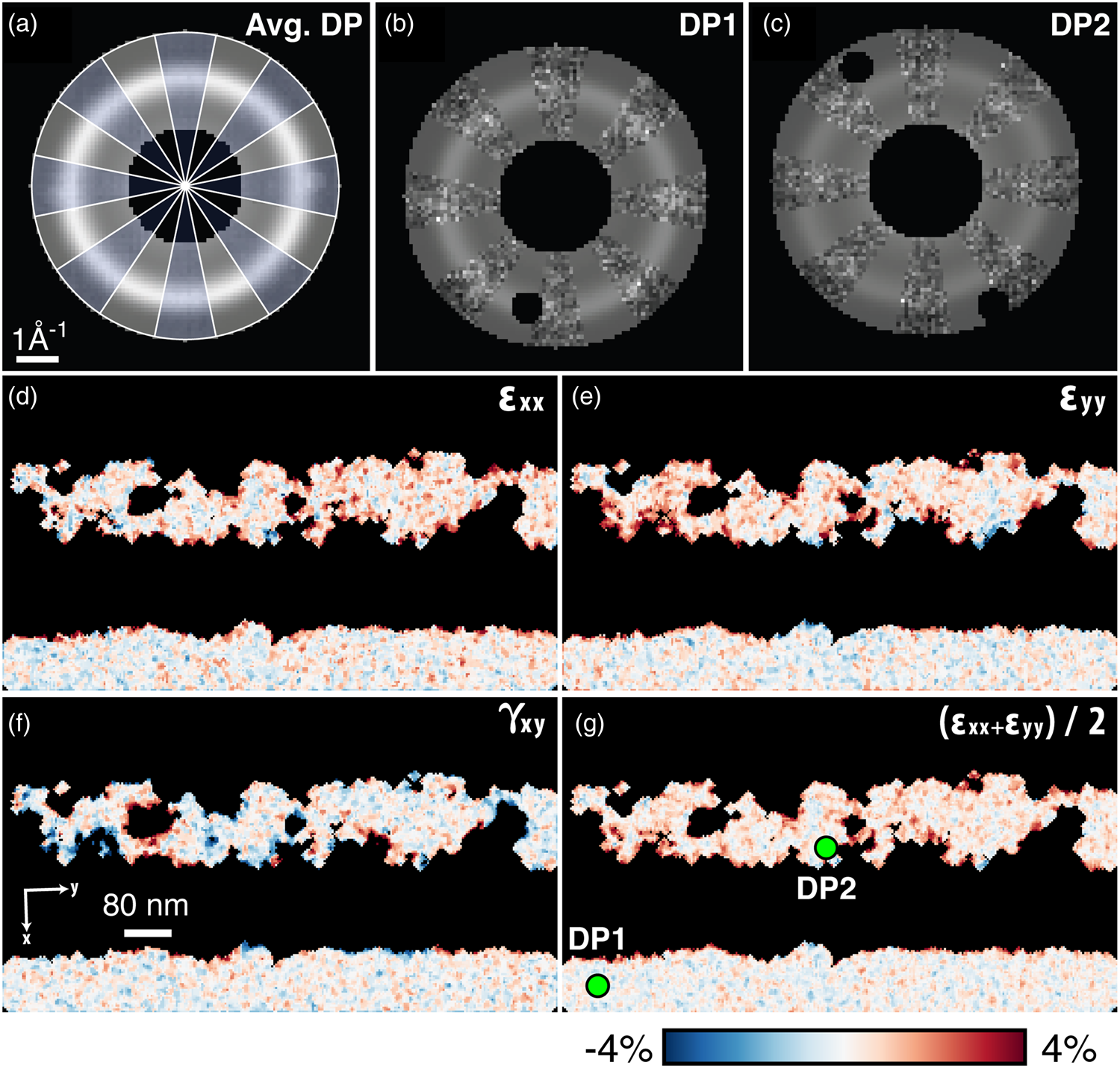
Fig. 12. Amorphous strain. (a–c) Elliptical fits to the average amorphous diffraction pattern, and two selected diffraction patterns. In (a), blue wedges show the data, while clear wedges show the fit function. In (b) and (c), the data and the fit are similarly interleaved, and Bragg scattering has been masked away to ensure good fitting. (d,e) The compressive/tensile strains ε xx and ε yy, the shear strain γ xy, and the dilation  ${1\over 2}( \epsilon _{xx} + \epsilon _{yy})$.
Figures 12d–12g show the strains computed beginning from these fits, then finding the deviation of the elliptical distortions from a reference. Here, the median of the fully amorphous region is used. As with crystalline strain mapping, the choice of reference is important and should be selected carefully based on the individual experiment. Figures 12d–12f, showing the compressive/tensile strains along the shown x- and y-directions as well as the shear strain, are comparable to the crystalline ε xx, ε yy, and ε xy plots from Figure 11. Figure 12g additionally shows  ${1\over 2}( \epsilon _{xx} + \epsilon _{yy})$, representing the local dilation of the structure. Across the four shown amorphous strain plots, we observe local structural changes, especially at the crystalline–amorphous interfaces.
Radial Distribution Functions
The radial distribution function (RDF), or g(r), describes the relative density of atoms some distance r from a given atomic position. Thus, the RDF characterizes the distribution of distances between atoms in a given material. It can serve as an important fingerprint for amorphous materials, as it gives information about the distance and density of neighboring shells of atoms, which depend on the material's structure, chemistry and defect density (Srolovitz et al., Reference Srolovitz, Egami and Vitek1981). In this section, we qualitatively discuss the calculation of the RDF, and the structure of the resulting plot. The formal discussion of our methods, which follow Mitchell & Petersen (Reference Mitchell and Petersen2012) and Mu et al. (Reference Mu, Wang, Feng and Kübel2016), are found in Appendix H.
The RDF can be directly determined from the average diffraction pattern of an amorphous material, as long as enough counts/images are collected to average out any local density fluctuations, and the probe convergence semi-angle is sufficiently small to not blur out the diffraction pattern (Egami & Billinge, Reference Egami and Billinge2003). An example of the mean diffraction pattern from amorphous silicon is shown in Figure 13a. A radial integral is then calculated, here using a polar-elliptical methods of the section “Polar transformation,” yielding the diffracted intensity as a function of distance from the optic axis. The resulting curve, I(k), is shown in Figure 13c. The important elements of this signal are (1) thermal diffuse background, resulting from thermal motion of the atoms and which dominates the behavior shown here at low k values, (2) the single atom scattering factors, describing the scattered intensity profiles which result from individual atoms and which dominate the behavior at high k values, and (3) the structure factor Φ(k), which describes the arrangement of atoms relative to one another in the material. By fitting the thermal background and atomic scattering factors, it is possible to calculate the structure factor, and from the structure factor, it is possible to calculate the RDF. Figures 13d and 13e show the computed structure factor and RDF, respectively. In gathering data for RDF analysis, it is important to capture high scattering angles to use in fitting the atomic scattering factors; therefore, fairly short camera lengths are recommended.

Fig. 13. Radial distribution function of amorphous silicon. (a) An average diffraction pattern. (b) The polar-elliptical transform of (a). (c) The radial intensity profile, calculated from (b). (d) The structure factor, calculated by determining and subtracting off the single atom scattering factor, and applying a bandpass mask to cut off high- and low-frequency noise. (e) The radial distribution function, calculated using the structure factor, showing the first few shells of Si atoms. Dashed lines show the first two RDF peak distances from a similar study on amorphous Si (Laaziri et al., Reference Laaziri, Kycia, Roorda, Chicoine, Robertson, Wang and Moss1999). Our nearest neighbor spacing and next-nearest neighbor spacing measurements are each somewhat smaller than the literature values, by 9 and 2%, respectively.
We ultimately invert the structure factor, a diffraction space quantity, to retrieve the RDF, a real space quantity. Bandpass filtering the structure factor before inversion may be used to cut off high- and low-frequency noise; here, we used a bandpass filter with sigmoidal cutoffs at low and high frequencies centered at 0.2 and 0.8 Å−1, respectively. The sampling of the RDF is determined by the maximum k values in the experimental data. In py4DSTEM, we therefore enable optional upsampling by padding the structure factor with zeros before inversion, which allows extraction of an RDF which is in principle arbitrarily smooth, to aid in visualizing the data. Importantly, that smoothness is for visualization purposed only and should not be over-interpreted: the highest frequencies at which true information has been transferred is set by the maximum k from the experimental data. In Figure 13e, the interpolated data is shown as the red curve, and the non-interpolated data which reflects the plot's true resolution are shown as black points.
Importantly, the measured and computed RDF will never be a perfect reflection of the true RDF. The algorithm used to convert raw data to a g(r) curve is part of the story here—incremental improvements can be achieved by optimizing various aspects, such as the polar-elliptical fitting and transformation, the background fitting, or the bandpass filtering. In addition to these, there are also limitations of the experiment itself, such as the finite size of the beam and inelastic scattering. One clear and important resulting difference between our measured RDF and what we expect from a true, physical RDF is the structure of the nearest-neighbor peak, that is, the first maximum in g(r). Physically, the RDF must be zero close to r = 0. Typically, as r increases, g(r) is expected to climb fairly sharply at the onset of the nearest-neighbor peak, then decay more slowly toward the first trough and the second shell. However, the first shell in our measured g(r) shows no such asymmetry, and instead resembles a smooth sinusoid. This is unsurprising, as it reflects insufficient high frequency information to capture the true structure of the initial peak. Collecting energy filtered data, minimizing the probe size, and capturing high SNR data out to large scattering angles are a few steps that might lead to more realistic measured RDFs.
Finally, we note that the background fit shown here is incorrect. This can be seen in Figures 13c and 13d. Here, we see that our background is above the first peak in the median intensity (Fig. 13c), and correspondingly the first maximum in the structure factor remains below zero (Fig. 13d). Fortunately, the modular, open-source design of py4DSTEM enables ongoing improvements, and we anticipate correcting these shortcomings in the RDF analysis module in a future version of the code.
Fluctuation Electron Microscopy
Fluctuation electron microscopy (FEM) is a method which, like RDF analysis, is used to characterize the structure of amorphous materials. In RDF analysis, the structure is typically considered out to distances of perhaps the first few shells of neighboring atoms, considered the “short-range order” regime. However, many amorphous materials have a substantial degree of structural ordering beyond the first few shells (Phillips, Reference Phillips1979). This property is referred to as “medium-range order” in materials science (Treacy & Gibson, Reference Treacy and Gibson1996; Gibson et al., Reference Gibson, Treacy and Voyles2000; Nakhmanson et al., Reference Nakhmanson, Voyles, Mousseau, Barkema and Drabold2001). When using 4D-STEM to study amorphous materials, the STEM probe size (set by the convergence semi-angle and/or probe defocus) can be tuned to match the size of atomic clusters. When these clusters deviate from a fully random distribution, Bragg scattering leads to “speckles” in the amorphous halo. The technique of quantifying the degree of variability as a function of scattering angle and probe size is called FEM (Voyles & Muller, Reference Voyles and Muller2002). In this section we qualitatively discuss FEM, and a mathematical treatment is in Appendix I.
Our approach follows the methods of Bogle et al. (Reference Bogle, Nittala, Twesten, Voyles and Abelson2010). The idea is to calculate the variance V(k) of the diffraction patterns as a function of scattering angle. With an appropriate normalization based on the radial intensity profiles (see the Appendix), the variance can be thought of as a metric of order. Consider the limiting cases: in a minimally ordered sample, the atomic distribution is completely homogeneous, leading to perfectly smooth diffracted rings and thus zero variance at a given scattering angle. In a maximally ordered sample, that is, a perfect crystal, the rings resolve into Bragg disks, so that the variance at some fixed k containing peaks will be maximized. The RDF is primarily sensitive to the two-body atomic pair correlations, whereas the FEM variance is more sensitive to four-body pair-pair correlations (Treacy & Gibson, Reference Treacy and Gibson1996; Rodenburg, Reference Rodenburg1999), hence its utility in examining medium-range order.
Figure 14 shows an FEM measurement of an amorphous silicon sample, performed in py4DSTEM. Figure 14a shows the mean diffraction pattern of the dataset, with two strong amorphous rings visible. However, plotting the maximum intensity across all probe positions, shown in Figure 14b, shows clear Bragg disk features. This is due to small regions of crystallinity, present in some small fraction of probe positions. This is important because which sample features dominate, or are apparent at all, is highly sensitive to exactly what signal is being examined; and in FEM analysis, there are several similar but distinct ways of extracting the FEM signal (Voyles & Abelson, Reference Voyles and Abelson2003). Here, we demonstrate this sensitivity, and show that using median statistics can be beneficial in targeting the amorphous signal in FEM analysis.

Fig. 14. Fluctuation electron microscopy of predominantly amorphous silicon. (a) An average diffraction pattern of the 4D-STEM scan, using median statistics. (b) A diffraction image generated by selecting the maximum value at each pixel across all scan positions, and revealing the presence of some amount of Bragg scattering, and therefore crystallinity, in this sample. (c) The radial intensity profiles of the dataset using median (red) and mean (blue) statistics, respectively. (d) The variance over all angles versus radial position. (e) V(q)/〈I(q)〉2, a measure of short and medium range order which becomes larger with increasing order. Note the two peaks in blue (mean statistics) which become a single broad peak in red (median statistics). These peaks come from Bragg scattering, suggesting that the median statistics are superior for evaluating the amorphous structure.
Figures 14c–14e respectively show the radial intensity profile, the variance, and the FEM signal, in each case using both mean and median statics. The presence of crystalline regions barely effects the mean intensity, but strongly modulates the variance V(k). The end result is the FEM signal in Figure 14e. This shows a strong signal at k = 0.318 Å−1 that corresponds to the distribution of nearest neighbor atoms in amorphous Si, with a mean scattering vector approximately equal to the crystalline Si [111] lattice spacing, and which is approximately the same using both mean and median statistics. In contrast, the FEM signal at higher scattering angles differs substantially using mean versus median statistics. With mean statistics, there are two strong peaks at k = 0.53 Å−1 and k = 0.62 Å−1, corresponding to the [220] and [311] crystalline Si diffraction peaks. Using median statistics, these two peaks are suppressed, revealing a lower intensity, broad amorphous peak hiding underneath them. This example highlights that the oversized impact even a small amount of Bragg scattering can have on FEM analysis, even in predominantly amorphous samples containing small amounts of crystal. In the particular use-case of small crystallites masking an amorphous signal of interest, median statistics are likely the simplest solution; note that other options, such as identifying and masking off Bragg scattering, are also possible. More broadly, this discussion suggests the importance of careful inspection of the diffraction images and careful choice of statistical methods in performing FEM data analysis.
Electron Phase Retrieval
py4DSTEM includes two methods for reconstruction of the sample potential: differential phase contrast (DPC) and ptychography. Broadly, the idea in both methods is to extract the phase factor that has been added to the electron beam wavefunction at each scan position. That phase is then taken to be the total (i.e., projected) sample potential at this scan position times a constant which encodes electron–charge interaction strength. Figure 15 shows the results of the py4DSTEM phase retrieval algorithms applied to a carbon nanotube, from Yang et al. (Reference Yang, Rutte, Jones, Simson, Sagawa, Ryll, Huth, Pennycook, Green, Soltau, Kondo, Davis and Nellist2016b).

Fig. 15. Phase retrieval of a carbon nanotube, using (a) differential phase contrast, or (b) single-side band ptychography. (c,d) The centers of mass of the diffraction patterns, used in DPC. (e) Convergence of the boundary condition correction component of the DPC algorithm. The scalebar corresponds to panel (a) and is in radians, see Appendix J. This dataset is found in Yang et al. (Reference Yang, Rutte, Jones, Simson, Sagawa, Ryll, Huth, Pennycook, Green, Soltau, Kondo, Davis and Nellist2016b).
These methods make the transmission function approximation as well as the projection approximation, and thus can be expected to be most reliable for thin, low-Z samples. In cases where these conditions do not hold, phase retrieval should be interpreted cautiously.
Differential Phase Contrast
DPC uses the fact that, for a sufficiently thin object, the mean deflection of the electron probe at each scan position in the STEM raster is related to the specimen electric and magnetic field components transverse to the beam propagation direction. Examples of material science applications of this technique include the study of built-in electric fields in semiconductor devices (Shibata et al., Reference Shibata, Findlay, Sasaki, Matsumoto, Sawada, Kohno, Otomo, Minato and Ikuhara2015), magnetic skyrmions (Matsumoto et al., Reference Matsumoto, So, Kohno, Sawada, Ikuhara and Shibata2016) and domain structures (Chapman et al., Reference Chapman, Batson, Waddell and Ferrier1978) and as a technique for efficient visualization of light atoms in materials (Song et al., Reference Song, Allen, Gao, Huang, Sawada, Pan, Warner, Wang and Kirkland2019). The technique, first suggested by Dekkers & De Lang (Reference Dekkers and De Lang1974), was extensively applied to the study of magnetic materials from the 1970s onward by Chapman and colleagues and has seen more ubiquitous use with the increased uptake of more sophisticated segmented detectors (Shibata et al., Reference Shibata, Findlay, Kohno, Sawada, Kondo and Ikuhara2012) and the advent of fast-readout electron cameras in STEM (Krajnak et al., Reference Krajnak, McGrouther, Maneuski, O'Shea and McVitie2016).
Figure 15a shows the DPC reconstruction of the sample. The mean probe deflections are shown in Figures 15c and 15d at each scan position in the x- and y-directions, respectively. Once these are calculated, optionally after defining some mask to cut off high-angle scattering, DPC considers this vector field of deflections to be the gradient of some scalar function. The primary task of DPC is, thus, to reconstruct the scalar field (a.k.a. the DPC image) which has as its gradient the measured probe deflections. In py4DSTEM, this inversion is accomplished by Fourier integration of the probe deflections (Arnison et al., Reference Arnison, Larkin, Sheppard, Smith and Cogswell2004; Close et al., Reference Close, Chen, Shibata and Findlay2015). This is performed iteratively; the convergence curve is shown in Figure 15e and shows that the computation has completed after 15 iterations. In the phase object regime (also known as the multiplicative approximation), the resulting scalar field is proportional to the sample potential. Appendix J derives the relation between the beam deflections and the sample potential and discusses the Fourier integration approach used. A consequence of Fourier integration is that it implicitly assumes periodic boundary conditions, which can be problematic for nonperiodic electron microscopy specimens. Boundary condition handling is important to a high-quality DPC reconstruction, and in py4DSTEM, we used an iterative boundary condition correction algorithm which is discussed in detail in Appendix J.
The rotational offset between real and diffraction space needs to be correctly calibrated to perform the Fourier integration step. One possibility is to use the method discussed in the section “Calibration” to determine the real/reciprocal rotational offset—that is, perform the calibration manually. Alternative approaches to automate this calibration are also possible using DPC methods—two are discussed here. In one method, we begin by observing that if the assumptions of DPC hold (primarily a thin enough specimen for the phase object approximation to be valid—see Appendix J), then the beam deflections scale with the gradient of the potential, and should therefore be a conservative vector field. In the presence of a relative rotation between real and reciprocal space, however, the measured beam deflections will all be similarly rotated, in general resulting in an apparently nonconservative field. The correct rotational offset can therefore be identified by finding the relative rotation which results in beam deflections which are conservative. Algorithmically this can be accomplished by calculating the curl as a function of the real/reciprocal rotation, then identifying the rotation which minimizes the curl as the correct rotational offset. In the second method, we note that the contrast of a DPC reconstruction is maximized when the rotational offset is correct. Thus, the calibration may also be performed by maximizing the DPC contrast as a function of real/diffraction space rotation. Note that this latter method permits a 180 degree ambiguity in the rotational offset, corresponding to a contrast reversal in the DPC image.
The DPC reconstruction is a scalar field which is calculated by Fourier integration of the beam deflections. We note that Fourier integration effectively applies a low-pass filter. Some amount of low-pass filtering is, therefore, inherent in DPC imaging as implemented in py4DSTEM.
Finally, we note that while DPC provides useful image contrast in a fairly wide array of contexts, physical interpretation, and in particular interpretation in terms of the local sample potential, should be undertaken with care. Under optimal conditions, the DPC image is a reflection of the phase added to the electron beam, which in turn reflects the sample potential. However, in many datasets under realistic experimental conditions, the signal in the DPC image result from any number of other effects and should not be conflated with the sample potential. The most common such effect is sample thickness—for thick samples, the phase object approximation does not apply, and the DPC signal is almost certainly not a representation of the true “phase” of the specimen due to strong multiple electron scattering. Additional important factors include the convergence angle, and the real space step size. With respect to the convergence angle, any sample structure smaller than the probe size cannot be resolved and will not be reflected in a DPC image—thus, if α is smaller than the Bragg angle, any atomic structure will be lost in the DPC image. With respect to the real space pixel size, if the spatial sampling is larger than the probe width, any variation in the potential in between sampling points will be effaced in the reconstruction.
A DPC image for thicker samples, or samples with small convergence angles or large step sizes, may still be physically informative. In these cases, DPC is a convenient technique for creating a high contrast map of the field of view and may be thought of as another flavor of virtual imaging. Images in this category might be referred to as “pseudo-DPC.” The DPC image in Figure 1 is a good example of this—the sample is thick, α is smaller than the Bragg angle, the beam step size is larger than the probe. This DPC image almost certainly does not reflect the sample potential; it does generate a high contrast image of a complex sample. In contrast, the DPC image shown in Figure 15a was generated from a very thin sample such that the phase object approximation is reasonable, with a large convergence angle and a real space step size smaller than the probe width. This is, therefore, a "true” DPC image and may be interpreted in terms of the sample potential. See Appendix J for further discussion.
Ptychography
Phase retrieval is difficult because phase is never directly recorded; instead, the detector only captures the square modulus of the electron wavefunction. In electron ptychography of crystals, the idea is that with a large enough convergence angle, the central disk will begin to overlap with other Bragg disks. In the overlap regions, the phases of the two beams add coherently, and consequently, phase reconstruction is possible by analyzing these regions. The method is analogous to holography, which combines a scattered beam and a reference beam to create an interference pattern, except that the “scattered” and “reference” beams are now the central beam and the Bragg reflected beams. Variations in these regions of interference as the beam is scanned enable phase retrieval. Ptychography was first suggested as a method to solve the crystallographic phase problem by Hoppe (Hoppe, Reference Hoppe1969a, Reference Hoppe1969b; Hoppe & Strube, Reference Hoppe and Strube1969), and later extended to solve the phase problem for arbitrary specimens by Rodenburg (Rodenburg & Bates, Reference Rodenburg and Bates1992).
py4DSTEM includes a ptychographic reconstruction algorithm which calculates the phase in a single step, based on the single-side band approach and discussed in detail in Appendix K. Figure 15b shows the results for the carbon nanotube discussed above, and clearly reveals both the walls of the tube as well as the tortuous structure of carbon inside the tube. In general, direct solvers tend to be fast, however, better reconstruction quality is usually achieved with iterative algorithms.
Conclusion
In this paper, we presented the py4DSTEM software package written in Python, for analysis of 4D-STEM experiments. We described the program's purpose and structure, including an HDF5-based file standardization for 4D-STEM. We described how py4DSTEM can be used for preprocessing and calibrating data, finding Bragg disk positions, transformation into polar-elliptical coordinates, and for classifying diffraction patterns based on commonalities in their diffraction patterns. We demonstrated measurements including virtual imaging, phase mapping, mapping strain in crystalline and amorphous materials, RDF and FEM analyses, and phase reconstruction with DPC and with ptychography. The analysis here spans eight datasets, including seven experimental and one synthetic dataset.
The py4DSTEM code and many examples are freely available in the py4DSTEM repository on Github. As an open-source project, both new users and new contributors are enthusiastically encouraged to try the code, use it in their own work, or make a contribution.
Acknowledgments
This project is supported by the Toyota Research Institute. Work at the Molecular Foundry was supported by the Office of Science, Office of Basic Energy Sciences, of the U.S. Department of Energy under Contract No. DE-AC02-05CH11231. BHS and LAH were supported by the Toyota Research Institute. SEZ and PP were supported by STROBE, an NSF Science and Technology Center, under Grant No. DMR 1548924. SZ was supported by the US Office of Naval Research under Grant No. N00014-17-1-2283. TCP acknowledges funding from the DFG-project BR 5095/2-1 (Compressed sensing in ptychography and transmission electron microscopy). JD was supported by the Dow University Partnership Initiative Program. YX was funded by under the U.S. Department of Energy Basic Energy Research Materials Sciences and Engineering Division Contract No. KC22ZH. MTJ and MMS were supported by the U.S. Department of Energy, Office of Science, Basic Energy Sciences, Materials Sciences and Engineering Division under award LANLE4BU. Los Alamos National Laboratory, an affirmative action/equal opportunity employer, is managed by Triad National Security, LLC, for the National Nuclear Security Administration of the U.S. Department of Energy under contract 89233218CNA000001. CO acknowledges support of an Department of Energy Early Career Research Award. HGB and JC acknowledge additional support from the Presidential Early Career Award for Scientists and Engineers (PECASE) through the U.S. Department of Energy. The authors thank Shreyas Cholia, Matthew Henderson, Rollin Thomas, and Ludovico Bianchi from the National Energy Research Scientific Computing Center (NERSC) for support with high-performance computing integration. NERSC is a U.S. Department of Energy Office of Science User Facility operated under Contract No. DE-AC02-05CH11231. The authors thank Blas Uberuaga for sample acquisition and support. Thanks also to the developers of Hyperspy, openNCEM, SciPy, NumPy, and Matplotlib, without whom this project would not have been possible.
Appendix A. Basic Formalism for 4D-STEM
Figure A.1 shows the geometry of an STEM experiment. We define the following probe wavefunctions:
 $$\eqalign{\Psi_{\rm 0} ( {\bf k}) & = \hbox{initial probe formed in diffraction space,} \cr \psi_{\rm 0} ( {\bf r}) & = \hbox{\,probe focused onto sample surface,} \cr \psi( {\bf r}) & = \hbox{\,probe at the exit plane of sample,} \cr \Psi ( {\bf k}) & = \hbox{\,far-field probe in the detector plane,}}$$
where r and k denote coordinates in the real space image and diffraction space planes, respectively, and the diffraction plane coordinate |k| = α/λ for scattering angle α and relativistically corrected electron wavelength λ. In an STEM experiment, scan coils are used to move the probe to a given position R, denoted by ψ0(r − R). In this appendix, we first describe a simple model for 4D-STEM datasets, which primarily refers to the diffraction plane wavefunction Ψ(R, k). We then briefly discuss the more general question of how the wavefunction evolves from the initial probe Ψ0 to the final probe Ψ on the detector.

Fig. A.1. Schematic of STEM experimental geometry, showing initial probe focused onto sample surface, propagating through sample, exiting the sample, and finally being imaged in the far-field detector plane.
A 4D-STEM dataset typically takes the form of a four-dimensional array of intensity values,
 $$\eqalign{I & = I_{i, j, n, m} \cr & = I( R_x,\; R_y,\; k_x,\; k_y) \cr & = I( {\bf R},\; {\bf k}).}$$
Here, each I i,j,n,m is a scalar and  $( i,\; j,\; n,\; m) \in {\opf N}$, that is, the dataset is a discrete 4D grid of numbers. The correspondences between (i, j) and scan position R = (R x, R y) and between (n, m) and diffraction coordinate k = (k x, k y) are determined by the real and diffraction space pixel size calibrations. The value of each I i,j,n,m is given by the electron flux passing through the appropriate detector pixel, or by the square modulus of the beam wavefunction integrated over the detector pixel at k when the beam raster position is R. Thus, the 4D-STEM dataset may be modeled by
 $$\eqalign{I( {\bf R},\; {\bf k}) & = \int_{k_x}^{k_x + \Delta k}\int_{k_y}^{k_y + \Delta k} \vert \Psi( {\bf R},\; {\bf k}) \vert^{2} \, dk_x\, dk_y\cr & \approx \vert \Psi( {\bf R},\; {\bf k}) \vert^{2},}$$
where the approximation is exact in the limit of infinitesimally small detector pixels. Note that this simple model does not account for finite information transfer in the microscope, which could be included with a multiplicative transfer function M(k).
In an STEM experiment with an integrating detector (ADF, BF, etc.), the image I(R) can be modeled as
 $$I( {\bf R}) = \int \vert \Psi( {\bf R},\; {\bf k}) \vert ^{2} D( {\bf k}) \, d{\bf k},$$
where D(k) reflects the detector geometry. For some 4D-STEM signal I(R, k), we can write down an equivalent virtual image I v(R) as:
 $$I_{\rm v}( {\bf R}) = \int I( {\bf k},\; {\bf R}) D( {\bf k}) \, d {\bf k}.$$
If equations (A.1) and (A.2) look similar, it is because they are. The key difference is in the meaning of the integration over D(k): in the former equation, it describes the action of the detector, and the integration occurs in hardware during data acquisition; in the latter equation, it is a prescription for which pixels of the 4D datacube need to be summed in post-processing.
The evolution of the probe is comparatively simple from the probe-forming aperture to the sample plane, and from the sample plane to the detector—both are given by Fourier transforms:
 $$\matrix{ \psi_0 ( {\bf r}) & = {\cal F}_{{\bf k}\to{\bf r}} \Psi_0 ( {\bf k}), \cr \Psi ( {\bf k}) & = {\cal F}_{{\bf r}\to{\bf k}} \psi ( {\bf r}), }$$
where  ${\cal F}_{{\bf r}\to {\bf k}}$ is the forward transform from the real to diffraction domain, and ${\cal F}_{{\bf k}\to {\bf r}}$ is the inverse transform from the diffraction to real domain. The most common initial condition for the electron probe in 4D-STEM is given by a circular aperture in a condenser plane
 $$\eqalign{\Psi_0 ( {\bf k}) & = A( k_{\rm max}), \cr & = \left\{\matrix{ 1, & {\rm if } \vert {\bf k}\vert \leq k_{\rm max}, \cr 0, & {\rm otherwise}, }\right.}$$
where A(k max) is the 2D “top hat” function, and k max is the maximum scattering vector of the probe. The probe incident on the sampe is then an Airy disk function
 $$\psi_0 ( {\bf r}) = {J_1 ( 2 \pi k_{\rm max} \vert {\bf r}\vert ) \over \sqrt{\pi} \vert {\bf r}\vert },$$
where J 1 is a Bessel function of the first kind, and the peak amplitude is equal to  $\sqrt {\pi } k_{\rm max}$. This function is shown graphically in the upper right corner of Figure A.1. More complex STEM probes can be formed by using amplitude-patterned apertures (Guzzinati et al., Reference Guzzinati, Ghielens, Mahr, Béché, Rosenauer, Calders and Verbeeck2019; Zeltmann et al., Reference Zeltmann, Müller, Bustillo, Savitzky, Hughes, Minor and Ophus2020), phase plates (McMorran et al., Reference McMorran, Agrawal, Anderson, Herzing, Lezec, McClelland and Unguris2011; Ophus et al., Reference Ophus, Ciston, Pierce, Harvey, Chess, McMorran, Czarnik, Rose and Ercius2016b; Yang et al., Reference Yang, Ercius, Nellist and Ophus2016a; Verbeeck et al., Reference Verbeeck, Béché, Müller-Caspary, Guzzinati, Luong and Den Hertog2018), or other methods (Blackburn & Loudon, Reference Blackburn and Loudon2014; Pozzi et al., Reference Pozzi, Lu, Tavabi, Duchamp and Dunin-Borkowski2017). In a vacuum, ψ0(r) = ψ(r), so that Ψ(k) and Ψ0(k) are identical up to scaling and phase factors, so that without a sample the image on the detector directly reflects the electron beam passing through the probe-forming aperture.
The change in the wavefunction from ψ0(r) to ψ(r), as the beam passes through a sample is, in general, analytically intractable, so numerical methods are typically used. Using some approximations described in Kirkland (Reference Kirkland2010), and omitting the scan coordinate R for clarity, the interaction of the STEM probe with the sample is governed by the time-independent Schrödinger equation
 $${\partial \psi( {\bf r}) \over \partial z} = {{{i\mkern 1mu}} \lambda\over 4 \pi} \left[{\partial^{2} \psi( {\bf r}) \over \partial x^{2}} + {\partial^{2} \psi( {\bf r}) \over \partial y^{2}} \right] + {{i\mkern 1mu}} \sigma V( {\bf r}) \psi( {\bf r}), $$
where  ${{i\mkern 1mu}}$ is the imaginary constant, σ is the relativistically corrected electron–matter interaction constant, and V(r) is the electrostatic potential inside the sample. The interaction constant σ is given by
 $$\sigma = {2\pi\gamma m_{\rm e} q_{\rm e} \lambda\over h^{2}},$$
where γ, m e, q e, λ, and h are the relativistic correction factor, the electron mass, the electron charge, and the relativistically corrected electron wavelength, and the Planck constant. Because the two operators on the right-hand side of equation (A.6) do not commute, it is typical to use a split-step method to numerically solve this equation called the multislice method, first derived in Cowley & Moodie (Reference Cowley and Moodie1957). To use the multislice method to solve the interaction of the electron beam with the sample, we first divide up the sample into a series of N slices, V n(r), which are 2D arrays that integrate all of the electrostatic potential contained in a given slice of thickness Δz, given by
 $$V_n( {\bf r}) = \int_{z - \Delta z/2}^{z + \Delta z/2} V( {\bf r}) \, dz.$$
By assuming that each slice has infinitesimal thickness, the solution to the transmission operator is given by
 $$\psi( {\bf r}) = T( {\bf r}) \psi_0( {\bf r}) = {\rm e}^{{{i\mkern 1mu}} \sigma V_n( {\bf r}) } \psi_0( {\bf r}).$$
Between each slice, we assume zero electrostatic potential and can, therefore, advance the electron wave by using the free-space propagation operator, which can be efficiently applied in Fourier space (Kirkland, Reference Kirkland2010)
 $$\psi( {\bf r}) = {\cal F}_{{\bf k}\to{\bf r}} \{ {\rm e}^{{{i\mkern 1mu}} \lambda \Delta z \vert {\bf k}\vert ^{2}} [ {\cal F}_{{\bf r}\to{\bf k}} \psi_0( {\bf r}) ] \}.$$
Note that the propagation operator  ${\rm e}^{{{i\mkern 1mu}} \lambda \Delta z \vert {\bf k}\vert ^{2}}$ uses the 2D inverse spatial coordinate ${\bf k} = {k_x}^{2} + {k_y}^{2}$. We alternate the application of the transmission and propagation operators to calculate the final wavefunction after interacting with the sample,
 $$\psi( {\bf r}) = \prod_{n = 1}^{N} \{ {\cal F}_{{\bf k}\to{\bf r}} [ {\rm e}^{{{i\mkern 1mu}} \lambda \Delta z \vert {\bf k}\vert ^{2}} \{ {\cal F}_{{\bf r}\to{\bf k}} [ {\rm e}^{{{i\mkern 1mu}} \sigma V_n( {\bf r}) } ] \} ] \} \psi_0( {\bf r}) ,\; $$
which is typically referred to as the exit wave. This method requires N transmission operations and N − 1 propagation operations. The multislice method is often used for modeling 4D-STEM experiments but can require a prohibitively high amount of computation time for very large simulations. Recently, a more efficient method has been developed to simulate 4D-STEM experiments called PRISM (Ophus, Reference Ophus2017), which has been made available as a simulation code (Pryor et al., Reference Pryor, Ophus and Miao2017), and extended to simulate electron energy-loss spectroscopy (STEM-EELS) inelastic scattering as well (Brown et al., Reference Brown, Ciston and Ophus2019).
Appendix B. Cross, Phase, and Hybrid Correlations
Cross-correlative template matching is a standard tool in image processing and is widely used in computational analysis for electron microscopy (Frank, Reference Frank1975; Modersitzki, Reference Modersitzki2004). The purpose of this appendix is to outline the formalism for these methods and to briefly discuss the effects of and appropriate uses cases for so-called hybrid correlations.
For functions f and g, written in one dimension for simplicity, the cross-correlation is defined as
 $$( f \star g) ( x) = \int_\infty^{\infty} f( y) ^{\ast }g( x + y) \, dy,$$
where  $\star$ indicates a cross-correlation and * indicates complex conjugation. The key idea here is that if f(x − a) = g(x), then $( f \star g) ( x = a)$ will be a maximum, because the integrand then becomes |f(y)|2 and two functions are perfectly overlapped. Therefore, the cross-correlation of the vacuum probe template with a diffraction pattern can be used to extract the Bragg disk positions simply by identifying the cross-correlation maxima.
Computationally, this is implemented via the cross-correlation theorem, which states that
 $$( f \star g) ( x) = {\cal F}^{-1}( ( {\cal F}f) ^{\ast } ( {\cal F}g) ), $$
where  ${\cal F}$ is the Fourier transform. This follows directly from the Fourier transform of equation (B.1) and the change of variables x′ = x + y. Equation (B.2) therefore allows the integral of equation (B.1) to be computed efficiently via a few FFT operations, which is important because performing the cross-correlation on each diffraction pattern (often 10,000 or more) is the most computationally intensive step of many analysis workflows.
In contrast to equation (B.2), the so-called phase correlation normalizes by the amplitude in Fourier space before applying the inverse transform:
 $$( f \star g) _{\rm phase}( x) = {\cal F}^{-1}\left({( {\cal F}f) ^{\ast } ( {\cal F}g) \over \vert( {\cal F}f) ^{\ast } ( {\cal F}g) \vert} \right).$$
This leads to an analytically pleasing result: now, if f(x − a) = g(x), then  $( f \star g) _{\rm phase}( x) = \delta ( x-a)$. The result follows directly from substituting f(x − a) = g(x) into equation (B.3) and making use of the Fourier shift theorem. Thus, where the cross-correlation simply has a maximum where f and g best overlap, the phase correlation yields a delta function which selects the point of interest. As a practical matter, however, phase correlations are also highly sensitive to noise, and this application tend to lead to many false positives when used with real data.
An intermediate approach is possible using a hybrid correlation, in which a normalization somewhere in between a phase and cross-correlation is used, as follows:
 $$( f \star g) _{n}( x) = {\cal F}^{-1}\left({( {\cal F}f) ^{\ast } ( {\cal F}g) \over \vert( {\cal F}f) ^{\ast } ( {\cal F}g) \vert^{1-n}} \right).$$
Here, n ∈ [0, 1]. For n = 1, the result is a cross-correlation, and for n = 0, the result is a phase correlation. Intermediate values may be thought of is applying intermediate weighting to the amplitude versus phase components of the signals in Fourier space. Note that computationally we implement equation (B.4) in the more numerically stable form  $( f \star g) _{n}( x) = \vert m \vert ^{n} \, {\rm e}^{{{i\mkern 1mu}}{\rm arg}( m) }$, where $m = ( {\cal F}f) ^{\ast } ( {\cal F}g)$. While the hybrid correlation is a heuristic approach, it is often effective. Giving more weight to the phase components (lower values of n) increases sensitivity to edges and can do a better job of identifying faint Bragg disks, however, the trade off is typically an increase in false-positives. Experience with many datasets indicates that an n value in the neighborhood 0.85 or 0.9—similar to a cross-correlation, but with a slightly increased sensitivity to edges—frequently yields good results. The noisier the data, the more caution is in order in using lower n values, and for very noisy data pure cross-correlations are recommended. Figure B.1 shows cross, hybrid (for several n values), and phase correlations in one dimension for simulated data with and without noise.

Fig. B.1. Cross-correlation, phase correlation, and hybrid correlation. A 1D vacuum probe has been correlated with a 1D comb of Bragg disks without (left) and with (right) noise. Various values of n are used, where n = 1 is a cross-correlation, n = 0 is a phase correlation, and intermediate values are “hybrid” correlations—see equation (B.4). Hybrid correlations increase sensitivity to edges and narrow the central maxima relative to a cross-correlation, but also increase sensitivity to noise.
Appendix C. Synthetic Probes
Synthetic probes generated in py4DSTEM take the form of a flat disk with an edge that decays to zero sigmoidally according to
 $$\psi( k) = {1\over 1 + \exp{4( k - k_0) \over w}}.$$
Here, k 0 is the radius of the disk, and w is the width over which the edge of the probe decays, falling from 88 to 12% of its maximum value of 1 in this span.
Appendix D. Bragg Vector Map Formalism
Let us refer to the ith Bragg disk detected in the diffraction pattern at scan position (R x, R y) as  ${\cal B}_{R_x, R_y, i}$. In computer memory, this might be thought of as a length 3 tuple: ${\cal B}_{R_x, R_y, i} = ( k_{x, i},\; k_{y, i},\; I_i)$, where the subscript i indicates the ith peak, and the three values are the coordinates of the disk center in diffraction space and the disk's intensity. Analytically, we can think of the ${\cal B}_{R_x, R_y, i}$ as Kronecker deltas of strength I i:
 $${\cal B}_{R_x, R_y, i}( {\bf k}) = I_i\delta( k_x - k_{x, i}) \delta( k_y - k_{y, i}). $$
The delta function specifies where the Bragg condition is met for parallel illumination; Bragg disks are formed by translating each point in the central disk by this vector and may be thought of as the convolution of the aperture function with equation (D.1).
Let us denote the set of all Bragg disks detected at a scan position (R x, R y) as  ${\cal B}_{R_x, R_y}$. For N disks in ${\cal B}_{R_x, R_y}$, we can write
 $${\cal B}_{R_x, R_y}( {\bf k}) = \sum_{i = 1}^{N} I_i\delta( k_x - k_{x, i}) \delta( k_y - k_{y, i}). $$
Taking a summation over all scan positions gives
 $${\cal B}( {\bf k}) = \sum_{r_x \in R_x}\sum_{r_y \in R_y} {\cal B}_{r_x, r_y}( {\bf k}), $$
 $$= \sum_{r_x, r_y, i} I_{r_x, r_y, i}\delta( {\bf k} - {\bf k}_{r_x, r_y, i}) ,$$ ${\cal B}$ is the Bragg vector map. Physically, is interpretable as a (unnormalized) distribution of measured Bragg vector directions found within the sample over the area of the 4D-STEM scan.
Appendix E. Elliptical Fitting and Transforms
In this appendix, we describe various elements of py4DSTEM that make use of or relate to elliptical coordinates. First, we discuss elliptical fitting, which is important for correction of elliptical distortions. We then briefly describe and relate the two elliptical parametrizations used in the code. Finally, we describe polar-elliptical transformations and radial integration.
Two primary elliptical fitting routines are available in py4DSTEM. The first is appropriate for data that is well-described by a 1D elliptical curve—for instance, a Bragg vector map from a sample with many randomly oriented grains will typically contain elliptical rings associated with each characteristic spacing of the material. The second is a sum of two Gaussian functions, a simple Gaussian and a “double-sided” Gaussian, and is appropriate for fitting amorphous diffraction patterns, and is a two-dimensional fit designed to capture the first amorphous halo.
For 1D elliptical curve fitting, we first define some annular region of our 2D dataset containing pixels  $( k_{x_i},\; k_{y_i})$, each with intensity I i. We then determine the ellipse that most closely fits this data by computing
 $$\eqalign{_{k_{x_0},\; k_{y_0},\; A,\; B,\; C}^{\arg\min} \sum_i [ & A( k_{x_i}-k_{x_0}) ^{2} \cr & \quad + B( k_{x_i}-k_{x_0}) ( k_{y_i}-k_{y_0}) \cr & \quad + C( k_{y_i}-k_{y_0}) ^{2} - 1] I_i.}$$
The double-sided Gaussian function for amorphous halo fitting is defined as
 $$\eqalign{& f( k_x,\; k_y\semicolon\; I_0,\; I_1,\; \sigma_0,\; \sigma_1,\; \sigma_2,\; c,\; R,\; k_{x_0},\; k_{y_0},\; B,\; C) \cr & \quad = {\cal N}( r\semicolon\; 0,\; \sigma_0,\; I_0,\; ) \cr & \qquad + {\cal N}( r\semicolon\; R,\; \sigma_1,\; I_1) \Theta( r-R) \cr & \qquad + {\cal N}( r\semicolon\; R,\; \sigma_2,\; I_1) \Theta( R-r), }$$
where (k x, k y) are the coordinates and  $( I_0,\; I_1,\; \sigma _0,\; \sigma _1,\; \sigma _2,\; c,\; R,\; k_{x_0},\; k_{y_0},\; B,\; C)$ are parameters, where ${\cal N}( r\semicolon\; R,\; \sigma ,\; I)$ is a Gaussian centered at R with standard deviation σ and with maximum amplitude I, where Θ is the Heaviside step function, and where r is the radial coordinate of an elliptical system given by $r^{2} = ( k_x-k_{x_0}) ^{2} + B( k_x-k_{x_0}) ( k_y-k_{y_0}) + C( k_y-k_{y_0})$. When performing a fit, as before we first define an annular region in the dataset to fit, typically about the first amorphous halo. The first term is meant to fit the decaying background, while the second and third terms fit the amorphous halo, while allowing for an asymmetrical shape on the inner/outer sides of the ring.
When fitting ellipses, we use the parametrization
 $$1 = A( k_x-k_{x_0}) ^{2} + B( k_x-k_{x_0}) ( k_y-k_{y_0}) + C( k_y-k_{y_0}) ^{2}$$
for numerical stability. However, the parameters of this form are not the most easily geometrically interpretable, so for this reason, we also make use of the alternate parametrization
 $$\matrix{k_x & = k_{x_0} + A'r\cos( \theta) \cos( \phi) - B'r\sin( \theta) \sin( \phi), \cr k_y & = k_{y_0} + B'r\cos( \theta) \sin( \phi) + A'r\sin( \theta) \cos( \phi)},$$
where (k x, k y) are cartesian coordinates, (r, θ) are polar-elliptical coordinates, and (A′, B′, ϕ) are parameters corresponding to the two semi-axis, and the tilt of the A′-axis with respect to the k x-axis. Equations (E.1) and (E.2) are related by
 $$\eqalign{A' & = \sqrt{{2\over A + C + \xi}}, \cr B' & = \sqrt{{2\over A + C-\xi}}, \cr \xi & = ( A-C) \sqrt{1 + \left({B\over A-C}\right)^{2}}, \cr \phi & = {1\over 2}\tan^{-1}\left({B\over A-C}\right).}$$
Once the appropriate elliptical parameters are known, polar-elliptical transformations may be performed. After specifying a range and sampling the new polar coordinates, each point (r, θ) is mapped to some (k x, k y) position in Cartesian space, from which a bilinear interpolation is then used to compute the value at (r, θ). In py4DSTEM, arrays returned after polar-elliptical transformation are numpy masked arrays, to ensure that coordinates beyond the frame of the raw data are correctly handled, as well as to facilitate masking data where necessary, for example, from a beamstop. Radial integrals are calculated by first computing the polar-elliptical (or polar) transformation then summing along the θ-direction.
Appendix F. Classification
The underlying principle of the classification scheme described in the section “Classification” is the definition of a particular feature vector, which is useful because it efficiently encodes the key physical features of crystalline electron scattering—the Bragg vectors. It therefore massively reduces the size of the data before classification, while honing in on the most physically relevant element of the diffraction data. For a calibrated Bragg vector map containing N delta-like peaks, we associate with each such peak an integer i ∈ {0, …, N − 1}. For each diffraction pattern, we generate a length-N vector v. The ith element of v is defined in one of two ways: (1) a Boolean value indicating whether this diffraction patterns contains this Bragg peak or (2) a floating point value of the intensity of this Bragg peak in this diffraction pattern.
With these feature vectors in hand, we use matrix factorization methods to complete the classification. First, we construct the matrix X which has the feature vectors v as its columns. For data with R N = R Nx × R Ny diffraction patterns, X has dimensions N × R N. X is then written as
 $$X = WH,$$
where W has shape N × C, H has shape C × R N, and C is the number of classes. W may be thought of as a collection of C column vectors, each describing a class in terms of weights for the various possible Bragg vectors observed over the entire dataset. H may be thought of as a set of column vectors which describe how to obtain, through linear combination of the classes, good approximations for each of the observed diffraction patterns. Alternatively, the row vectors of H may be thought of as an image (albeit reshaped): there are C of them, and each describes how much to weight the corresponding class in each of the R N positions of the electron beam.
A crucial question is: how to initialize the classes? In particular, the final result is generally quite sensitive to the number of classes. In the sections “Classification” and “Structural phase mapping,” we use an algorithm based on the frequency of co-occurrence of Bragg peaks across diffraction patterns to set initial values for W and H. The initialization algorithm begins by finding the pair of diffraction patterns with the most shared Bragg peaks. Then, we determine the fraction of those shared peaks which are contained in every other diffraction pattern, find the one with the greatest co-occurrence, and choose to add it or not add it to the group if its fraction of shared peaks is above a threshold. This process continues, adding more diffraction patterns to the group, until the best candidate pattern shares an insufficient fraction of its Bragg peaks with the group. At this point, a new group is seeded, by examining only those diffraction patterns which have not already been assigned to a group, and again finding the pair with the most co-occurring peaks. These groups are then converted into the W matrix using Boolean values to represent each diffraction pattern being in or out of a class in a given column, and H is calculated using X and W with a non-negative least squares solver. Finally, these initial classes may be optimized using non-negative matrix factorization (Pedregosa et al., Reference Pedregosa, Varoquaux, Gramfort, Michel, Thirion, Grisel, Blondel, Prettenhofer, Weiss, Dubourg, Vanderplas, Passos, Cournapeau, Brucher, Perrot and Duchesnay2011).
This initialization algorithm is simple and can assuredly be improved upon. Still, we have found it to be effective in a number of use cases, including the twin boundary shown in Figure 8 and the complex Gd2Ti2O7 shown in Figure 10.
Appendix G. Strain
In this appendix, we discuss how the crystalline and amorphous strains are calculated in the sections “Crystalline strain mapping” and “Amorphous strain mapping.”
We are interested in the infinitesimal strain matrix, where the deformed lattice differs very little from the undeformed lattice. For a material with a deformed state characterized by some displacement field u, and considering the system in a coordinate system with abscissa and ordinate (x 1, x 2), the infinitessimal strain matrix is
 $${\bf \epsilon} = \left(\matrix{\epsilon_{11} & \epsilon_{12} \cr \epsilon_{21} & \epsilon_{22} }\right) = \left(\matrix{{\partial u_1\over \partial x_1} & {1\over 2}\left({\partial u_1\over \partial x_2} + {\partial u_2\over \partial x_1}\right)\cr {1\over 2}\left({\partial u_1\over \partial x_2} + {\partial u_2\over \partial x_1}\right)& {\partial u_2\over \partial x_2} }\right)$$
and is typically accompanied by  $\theta _R = {1\over 2}( {\partial u_1}/{\partial x_2} - {\partial u_2}/{\partial x_1})$. The ε ii terms represent the compressive/tensile strain along the $\widehat {{\bf x}}_i$ directions, with positive values corresponding to tension. ε 12 represents the shear strain, and our sign convention is chosen such that positive values correspond to the angle spanned from $\widehat {{\bf x}}_1$ to $\widehat {{\bf x}}_2$ becoming more obtuse in the deformed body. θ R represents the rotation of the material, with positive values corresponding to counterclockwise rotation of a right-handed coordinate system.
For both crystalline and amorphous strain, the strain matrix is calculated at each beam position by comparing two comparable measurements: one of the local structure and one of an undeformed reference structure. For crystalline strain, the measurement we use is a pair of reciprocal lattice basis vectors. For amorphous strain, the measurement is a transformation of the ellipse fit to the (first) amorphous halo.
For crystalline strain, consider a real space lattice with reference basis vectors  $a^{0} = ( {\bf a}^{0}_1,\; {\bf a}^{0}_2)$ and local, deformed lattice vectors a = (a1, a2). The transformation matrix $T_{a^{0} \to a}$ describes the linear deformation of the space, and given the lattice vectors is calculable via
 $$a = T^{a} a^{0}.$$
The strain matrix in equation (G.1) is defined with respect to some arbitrary area element of the material under study, so we consider a square unit area element with sides  $( \widehat {{\bf e}}^{0}_1,\; \widehat {{\bf e}}^{0}_2) = ( \widehat {{\bf x}}_1,\; \widehat {{\bf x}}_2)$. The transformation T a maps these to a new set of vectors (e1, e2). In the limit of small area elements, the relevant derivatives are then expressible as
 $$\eqalign{{\partial u_1\over \partial x_1} & = ( {\bf e}_1 - {\bf e}^{0}_1) \cdot \widehat{{\bf e}}^{0}_1 = T^{a}_{11} - 1, \cr {\partial u_1\over \partial x_2} & = ( {\bf e}_1 - {\bf e}^{0}_1) \cdot \widehat{{\bf e}}^{0}_2 = T^{a}_{21}, \cr {\partial u_2\over \partial x_1} & = ( {\bf e}_2 - {\bf e}^{0}_2) \cdot \widehat{{\bf e}}^{0}_1 = T^{a}_{12}, \cr {\partial u_2\over \partial x_2} & = ( {\bf e}_2 - {\bf e}^{0}_2) \cdot \widehat{{\bf e}}^{0}_2 = T^{a}_{22} - 1,}$$
ε can then be retrieved from T a.
In practice, we calculate basis lattice vectors of the reciprocal lattice g = (g1, g2), by performing an intensity-weighted fit to measured Bragg peak positions at each scan position. The corresponding reference vectors  $g^{0} = ( {\bf g}^{0}_1,\; {\bf g}^{0}_2)$ can be determined several ways, including defining a reference region, dataset, or using a known crystal structure. At this point, it is possible to use g to determine a, then compute ε with the methods above. Alternatively, assuming sufficiently small deformations that we may discard terms of second order and higher in a Taylor expansion in both rotation and scaling, it is possible to compute ε directly from the transformation $T_{g^{0} \to g}$, describing the linear deformation of reciprocal space, with remarkably little alteration to the above equations. In this case, the final expressions for the strain are
 $$\matrix{ \epsilon_{11} & = 1 - T^{g}_{11}, \cr \epsilon_{22} & = 1 - T^{g}_{22}, \cr \epsilon_{12} & = - {1\over 2}( T^{g}_{12} + T^{g}_{21}), \cr \theta_{R} & = {1\over 2}( T^{g}_{12} - T^{g}_{21}).}$$
To measure strain from the diffraction pattern of an amorphous material, we fit ellipses at each probe position using the methods described in Appendix E. After shifting the origin of each ellipse to k = (0, 0), we have
 $$q_{\rm {ref}}^{2} = A {k_x}^{2} + B k_x k_y + C {k_y}^{2},$$
where q ref is a reference radius, which defines an undeformed (circular) amorphous halo given by
 $$q_{\rm {ref}}^{2} = {k_x}^{2} + {k_y}^{2}.$$
Because the measurement takes place in reciprocal space, it is more convenient to define the transformation matrix from the measured ellipse given by equation (G.4) to the reference circle given by equation (G.3), which is given by
 $$\left[\matrix{{k_x}' \cr {k_y}' }\right] = {\bf T} \left[\matrix{k_x \cr k_y }\right],\; $$
where
 $${\bf T} = {1\over \sqrt{A + C + W}} \left[\matrix{A + {1\over 2} W & B/2 \cr B/2 & C + {1\over 2} W }\right],\;$$
where
 $$W = \sqrt{4 A C - B^{2}}.$$
This expression is valid as long as the roots are real, that is, 4 A C − B 2 > 0. To calculate the strain deformation tensor, we proceed in a similar manner to (G.2), although we note the direction of the transformation has already been changed to the real space transformation directions,
 $$\matrix{ \epsilon_{11} & = T_{11} - 1,\cr \epsilon_{22} & = T_{22} - 1,\cr \epsilon_{12} & = {1\over 2}( T_{12} + T_{21}). }$$
The full expressions for the strain tensor components are
 $$\matrix{ \epsilon_{11} & = {A + {1 \over 2}W\over \sqrt{A + C + W}} - 1, \cr \epsilon_{22} & = {C + {1 \over 2}W\over \sqrt{A + C + W}} - 1,\cr \epsilon_{12} & = {B\over 2\sqrt{A + C + W}}. }$$
Taking a first order Taylor expansion about A = 1, C = 1, and B = 0 yields the linear strain approximation
 $$\matrix{ \epsilon_{11} & = {1\over 2}( A - 1), \cr \epsilon_{22} & = {1\over 2}( C - 1 ), \cr \epsilon_{12} & = {1\over 2} B.}$$
Note that when using the linear approximation above, it is important to use a value for q ref that is very close to the reference lattice average scattering radius, as the accuracy of the above expressions will suffer as the approximations A ≈ 1 and C ≈ 1 become worse.
An alternative method of determining the real space strains corresponding to an ellipse can be done using the matrix notation. In the matrix form, the ellipse equation (G.3) can be represented as
 $$M = \left[\matrix{A & B/2 \cr B/2 & C }\right],\; $$
where the major and minor axis directions are the eigenvectors of M, and their lengths are the square root of the eigenvalues. In the eigenbasis reference frame then, the transformation matrix, T, is simply the square root of the diagonalized eigenvalues, aligned with the corresponding eigenvectors. However, this must be rotated back to the traditional xy reference frame, or another chosen reference frame, via tensor rotation
 $${\bf T}' = {\bf R}{\bf T}{\bf R}^{\rm {T}},$$
where R is a standard rotation matrix and the superscript T represents transpose. The angle with respect to the xy-axis can be found by taking the two-argument arctangent (atan2) of an eigenvector. Finally, once T′ is in the correct orientation, the strains are simply
 $$\matrix{ \epsilon_{11} & = T_{11} - 1,\cr \epsilon_{22} & = T_{22} - 1,\cr \epsilon_{12} & = ( T_{12} + T_{21}) /2.}$$
We also note that most experiments will contain some degree of ellipticity even when no strain is present. In these cases, we will subtract the reference strain state from all measurements.
Appendix H. Radial Distribution Functions
We compute the radial distribution function following the methods of Mitchell & Petersen (Reference Mitchell and Petersen2012) and Mu et al. (Reference Mu, Wang, Feng and Kübel2016). Beginning from an amorphous diffraction pattern, often averaged over many probe positions to increase the SNR, we measure the radial intensity  $\langle I( k) \rangle _\phi$ averaged over the angular direction ϕ. Figures 13a–13c show such data for amorphous silicon. Next, we estimate the structure factor using the expression
 $$\Phi( q) = { \langle I( q) \rangle_\phi - I_{\rm {BG}}( q) - N \langle {\,f( q) }^{2} \rangle\over N \langle {\,f( q) }^{2} \rangle} q M( q) ,\; $$
where I BG(q) is a background intensity estimate, 〈f(q)2〉 is the mean-square of the parameterized single-atom scattering factors for all atomic species present, multiplied by N total atoms in the probe volume, and M(q) is a masking function. The single-atom scattering term is typically fit to the high scattering angle region, past the region where oscillating structure factor peaks are visible. The background I BG(q) can be an additional constant offset, a more complex fitting function, or just neglected. A masking envelope function M(q) is required to zero the structure factor Φ(q) at low scattering angles due to residual intensity from the central beam. This function can also be used to zero the structure factor Φ(q) at high scattering angles as well, due to residual fitting errors in N〈f(q)2〉 and I BG(q). Figure 13c shows the single-atom scattering fit, and Figure 13d shows the masked structure factor.
Next, we obtain the reduced RDF g(r) by taking the discrete (type II) sine transform of Φ(q), equal to
 $$g( r) = \sum_{q = 0}^{q_{\rm {max}}} \Phi( q) \sin \left[{\pi\over q_{\rm {max}}} \left({q\over \Delta q} + {1\over 2} \right)\left({r\over \Delta r} + 1 \right)\right],\; $$
where q max is the maximum q where Φ(q) is nonzero, and Δq and Δr are the pixel sizes in diffraction and real space, respectively. g(r) should ideally approach 0 as r → 0 within the nearest-neighbor shell, and approach 1 as r → ∞, but errors in the above fitting procedure can cause deviations from these results. Other authors recommend subtracting a 4th order polynomial from Φ(q) in order to reduce low spatial frequency artifacts (Mu et al., Reference Mu, Wang, Feng and Kübel2016). Here, we add a sigmoidal damping mask which clamps the RDF to zero as r → 0. Figure 13e shows the final result of the calculation, g(r).
Finally, we can also compute the atomic density ρ(r) of our sample using the expression
 $$\rho( r) = r [ g( r) + 4 \pi r \rho_0] ,\; $$
where ρ 0 is the bulk atomic density of the sample. This expression can be used to determine the coordination number of neighboring shells of atoms, by integrating over the distances r corresponding to a specific shell.
Appendix I. Fluctuation Electron Microscopy
The FEM computation here follows the methods of Bogle et al. (Reference Bogle, Nittala, Twesten, Voyles and Abelson2010). The first steps are identical to an RDF study, namely calibrating the elliptic distortions, performing the polar transformation, and measuring the average intensity as a function of scattering angle 〈I(q)〉ϕ,R from all diffraction patterns at probe positions R. Next, we measure the variance V(q) of the intensity as a function of scattering angle over all diffraction patterns
 $$V( q) = \langle [ \langle I( q) \rangle_{\phi} - \langle I( q) \rangle_{\phi, {\bf R}} ] ^{2} \rangle_{{\bf R}}.$$
In order to reduce the effect of thickness when comparing multiple datasets, we then compute the normalized variance V norm(q) as
 $$V_{\rm {norm}}( q) = { V( q) \over \langle I( q) \rangle_{\phi, {\bf R}}^{2} },$$
The RDF measurement described above is primarily sensitive to the two-body atomic pair correlations, whereas the FEM variance is more sensitive to four-body pair-pair correlations (Treacy & Gibson, Reference Treacy and Gibson1996).
Appendix J. Differential Phase Contrast
The notion of DPC is to select the detector function D(k) = k, referred to variously as a first moment or center-of-mass detector. Under this choice, in combination with the transmission function and weak object approximations, the center-of-mass image is related to the projected potential of the sample V(r) by
 $${\bf I}( {\bf R}) = {\sigma\over 2\pi} {\bf \nabla}V( {\bf r}) \ast \vert\psi_0( {\bf R}) \vert^{2}.$$
In this appendix, we derive equation (J.1), following Waddell & Chapman (Reference Waddell and Chapman1979), then summarize our own implementation. Note that in traditional DPC, a segmented detector is used to approximate I(R). In 4D-STEM, the center-of-mass of each diffraction pattern is computed instead. Comparison of these approaches can be found in Müller-Caspary et al. (Reference Müller-Caspary, Krause, Winkler, Béché, Verbeeck, Van Aert and Rosenauer2019).
Following Appendix A, let us first substitute in D(k) = k into (A.1), giving the (vector) image
 $${\bf I}( {\bf R}) = \int \vert \Psi( {\bf k},\; {\bf R}) \vert^{2} {\bf k}\, d{\bf k}.$$
Invoking that the real and diffraction planes are related by Fourier transforms [equation (A.3)], we can write
 $$\eqalign{{\bf I}( {\bf R}) & = \int \vert {\cal F}_{{\bf r}\to{\bf k}}( \psi( {\bf r},\; {\bf R}) ) \vert^{2} {\bf k} \, d{\bf k}\cr & = \int {\cal F}_{{\bf r}\to{\bf k}}( \psi( {\bf r},\; {\bf R}) ) {\cal F}^{\ast }_{{\bf r}\to{\bf k}}( \psi( {\bf r},\; {\bf R}) ) {\bf k} d{\bf k} \cr & = {1\over 2\pi i} \int {\cal F}_{{\bf r}\to{\bf k}}( {\bf \nabla}_{\bf r}\psi( {\bf r},\; {\bf R}) ) \cr & \quad \times {\cal F}^{\ast }_{{\bf r}\to{\bf k}}( \psi( {\bf r},\; {\bf R}) ) \, d{\bf k},}$$
where * indicates a complex conjugation, and in the last line, the derivative property of the Fourier transform has been invoked.Footnote 2
So far, no assumptions have been made. We now model the probesample interaction as multiplication of the electron wave function with a specimen transmission function T(r)Footnote 3 so that
 $$\eqalign{{\bf I}( {\bf R}) & = {1\over 2\pi i} \int d{\bf k} \int d{\bf r} {\rm e}^{-2\pi i{\bf k}\cdot{\bf r}} \cr & \quad \times ( \psi_0( {\bf r}-{\bf R}) {\bf \nabla}T( {\bf r}) + T( {\bf r}) {\bf \nabla}\psi_0( {\bf r}-{\bf R}) ) \cr & \quad \times \int d{\bf r}' \, {\rm e}^{2\pi i{\bf k}\cdot{\bf r}'} \psi^{\ast }_0( {\bf r}-{\bf R}) T^{\ast }( {\bf r}') \cr & = {1\over 2\pi i} \int d{\bf r} ( \vert\psi_0( {\bf r}-{\bf R}) \vert^{2} {\bf \nabla}T( {\bf r}) T^{\ast }( {\bf r}) \cr & \quad + {\bf \nabla}_{\bf r}\psi_0( {\bf r}-{\bf R}) \psi^{\ast }_0( {\bf r}-{\bf R}) \vert T( {\bf r}) \vert^{2} ) .}$$
Taking the phase object approximation, that is, T(r) = eiσV(R), the second half of the sum in equation (J.3) becomes
 $$\eqalign{& {1\over 2\pi i} \int d{\bf r} {\bf \nabla}_{\bf r}\psi_0( {\bf r}-{\bf R}) \psi^{\ast }_0( {\bf r}-{\bf R}) \cr & \quad = {\hbar\over 2\pi} \int d{\bf r} \psi^{\ast }_0( {\bf r}-{\bf R}) {\bf \widehat{\,p}} \psi_0( {\bf r}-{\bf R}) \cr & \quad = {\hbar\over 2\pi} \langle {\bf p} \rangle,}$$
where 〈p〉 is the expectation value of the probe momentum, and we made use of the fact that the momentum operator is  ${\bf \widehat {p}} = {1\over i\hbar }{\bf \nabla }$. But 〈p〉 is independent of R and thus provides some constant offset to I(R), and can be neglected. Meanwhile, the first half of equation (J.3) gives
 $$\eqalign{{\bf I}( {\bf R}) & = {1\over 2\pi i} \int d{\bf r} \vert\psi_0( {\bf r}-{\bf R}) \vert^{2} ( i\sigma {\bf \nabla}V( {\bf r}) ) \cr & = - {\sigma\over 2\pi} \int d{\bf r} \vert\psi_0( {\bf r}-{\bf R}) \vert^{2} {\bf E}( {\bf r}) ,}$$
where the second line uses  ${\bf E} = -{\bf \nabla }V$. Letting * denote a convolution, we arrive at
 $$\eqalign{{\bf I}( {\bf R}) & = {\sigma\over 2\pi} {\bf \nabla}V( {\bf r}) \ast \vert\psi_0( {\bf R}) \vert^{2} \cr & = - {\sigma\over 2\pi} {\bf E}( {\bf R}) \ast \vert\psi_0( {\bf R}) \vert^{2}.}$$
The first line is recognized as equation (J.1).
To solve for V given I(R) requires that we integrate equation (J.1). Following Arnison et al. (Reference Arnison, Larkin, Sheppard, Smith and Cogswell2004), Close et al. (Reference Close, Chen, Shibata and Findlay2015), Lazić et al. (Reference Lazić, Bosch and Lazar2016), and assuming a delta function probe wavefunction, we find
 $$\matrix{ {\bf I}( {\bf R}) & = {\sigma\over 2\pi}{\bf \nabla}V( {\bf R}) \cr {\cal F}_{{\bf R}\to{\bf k}}( {\bf I}( {\bf R}) ) & = i\sigma {\bf k}\cdot{\cal F}_{{\bf R}\to{\bf k}}( V( {\bf R}) ) \cr V( {\bf R}) & = {\cal F}^{-1}_{\bf k\rightarrow R} \left.\left[{{\bf k}\cdot{\cal F}_{\bf R\rightarrow k}\{ {\bf I}( {\bf R}) \} \over k^{2}}\right]\, \right/ i\sigma. }$$
In Figure 15a, the DPC reconstruction shown is in units of radians, corresponding to the quantity σV(R). We note that instead of assuming a delta-like probe, the probe wavefunction may be deconvolved from the image (Brown et al., Reference Brown, Shibata, Sasaki, Petersen, Paganin, Morgan and Findlay2017), however, we neglect this step because it serves to amplify noise in most experimental datasets. Computationally, when we compute the DPC image we modify equation (J.4) slightly by adding low- and high-pass regularization terms:
 $$V( {\bf R}) = {\cal F}^{-1}_{\bf k\rightarrow R} \left.\left[{{\bf k}\cdot{\cal F}_{\bf R\rightarrow k}\{ {\bf I}( {\bf R}) \} \over \lambda_1 + k^{2} + \lambda_2k^{4}}\right]\, \right/ i\sigma.$$
An additional challenge is the implicit assumption of periodic boundary conditions in the use of fast Fourier transforms to solve equation (J.4). This is demonstrated in Figure J.1 for reconstruction of a test image, a holographic reconstruction of a biological cell in saline from Müller et al. (Reference Müller, Schürmann, Girardo, Cojoc and Guck2018), shown in Figure J.1a. The x and y numerical derivatives of a cropped region (indicated by a white dashed outline) of Figure J.1a are shown in Figures J.1b and J.1c, respectively, and the result of the solution proposed in equation (J.4) is shown in Figure J.1d. An artifact of the implicit periodic boundary conditions can be seen in part of the white cell on the right-hand side of the frame appearing on the opposite left-hand side as indicated by a red arrow in Figure J.1d. The approach used in py4DSTEM to remedy this is to solve equation (J.4) on a larger grid that has been “padded” with zeros, as shown in Figure J.1e. The original grid corresponding to the input derivatives in Figure J.1 is indicated by a white dashed outline in Figure J.1. The gradient of the solution in Figure J.1e is taken and the result subtracted from the input derivatives shown in Figures J.1b and J.1c. The result of this subtraction (the residual) forms the input for another solution of equation (J.4) on a padded grid which is added to the phase solution as a correction. This processes is iterated upon until convergence. The result of just 10 iterations is shown in Figure J.1f, a more faithful reproduction of Figure J.1a than Figure J.1d.

Fig. J.1. Boundary condition handling for DPC. (a) A test image, an optical holographic reconstruction of a biological cell in saline from Müller et al. (Reference Müller, Schürmann, Girardo, Cojoc and Guck2018) along with the numerical derivatives of a cropped region (white dashed line) of the image in (b) and (c). (b,c) The DPC images. A DPC reconstruction from these produces (d), which has artifacts, most noticeably where indicated with a red arrow. The artifacts result from the boundary conditions implicitly assumed by the use of fast Fourier transforms. (e) The approach implemented in py4DSTEM, discussed in the body text, is to reconstruct on a padded grid [the original grid of (b) and (c) is indicated by the dashed outline]. The result of 10 iterations is shown in (f) which does not exhibit the same artifacts as (d).
Appendix K. Ptychography
In this appendix, we summarize the mathematics of the ptychographic reconstruction method implemented in Figure 15. Beginning from the transmission function approximation, the measured intensity I at a spatial frequency k and a probe position R is given by
 $$I( {\bf k},\; {\bf R}) = \left\vert \int \psi_0( {\bf r}-{\bf R}) T( {\bf r}) \, {\rm e}^{2 \pi i {\bf r}\cdot{\bf k}} \, d{\bf r}\right\vert ^{2}.$$
The goal is to retrieve T from I.
We first consider the transformed datacube  $I( {\bf k},\; {\bf K}) = {\cal F}_{{\bf R}\to {\bf K}}I( {\bf k},\; {\bf R})$, where K is the reciprocal coordinate to scan position R. Thus, this is the datacube has been written in terms of scan frequencies. Assuming that the sample is a weak phase object, this may be written as Rodenburg et al. (Reference Rodenburg, McCallum and Nellist1993)
 $$\eqalign{I( {\bf k},\; {\bf K}) & = \vert \Psi_{0}( {\bf k}) \vert ^{2}\delta( {\bf k}) \cr & \quad + \Psi_{0}( {\bf k}) \Psi_{0}^{\ast }( {\bf k} + {\bf K}) T( -{\bf k}) ^{\ast } \cr & \quad -\Psi_{0}^{\ast }( {\bf k}) \Psi_{0}( {\bf k}-{\bf K}) T( {\bf k}) ,}$$
where  $T( {\bf k}) = {\cal F}_{{\bf r}\to {\bf k}}T( {\bf r})$. The latter two terms in this expression each contain two copies of the aperture function, one centered at the optic axis and one shifted by the scan frequency K. For some given K, these terms can each be nonzero only at values of k where both disks are nonzero; that is, in the overlap between the shifted and unshifted disks. By looking only at the nonzero overlap between two disks, it is possible to simplify and solve equation (K.2) by eliminating one of its terms.
To eliminate the third term, define the set of pixels
 $${\cal K} = \{ {\bf k}\, \, \colon \, \, ( \vert{\bf k}\vert < k_0) \land\, ( \vert{\bf k} + {\bf K}\vert < k_0) \land\, ( \vert{\bf k}-{\bf K}\vert > k_0) \},$$
where  $\land$ is the logical and operation and the maximum disk size is k 0 = α/λ for convergence semi-angle α and electron wavelength λ. Here, the first line requires that k is inside the central disk, the second line requires that k is inside the disk shifted by − K, and the third line requires that k is also outside the disk shifted by K. Thus, ${\cal K}$ selects a region of double overlap while also excluding the region of triple overlap.
If only data from  ${\bf k} \in {\cal K}$ is used, the third term in equation (K.2) vanishes, so that
 $$T( -{\bf k}) ^{\ast } = \sum_{{\bf k} \in {\cal K}} {I( {\bf k},\; {\bf K}) \over \Psi_{0}( {\bf k}) \Psi_{0}^{\ast }( {\bf k} + {\bf K}) },\; $$
and T(r) can be obtained with a subsequent inverse Fourier transform. Since this uses only data from a single double-overlap region, this method has been dubbed single-side band reconstruction.
This approach can be extended to include data from the whole bright-field in the reconstructions. If the sample is a weak phase object, it obeys Friedel symmetry, so that T(k) = T( − k) * (Rodenburg et al., Reference Rodenburg, McCallum and Nellist1993). Inserting this into equation (K.2) and solving gives (Yang et al., Reference Yang, Ercius, Nellist and Ophus2016a)
 $$T( {\bf k}) = \sum_{{\bf k}\, \, \colon \, \, \vert{\bf k}\vert < k_0}I( {\bf k},\; {\bf K}) \cdot{\Gamma^{\ast }( {\bf k},\; {\bf K}) \over \vert \Gamma( {\bf k},\; {\bf K}) \vert ^{2}},\; $$
where Γ is the disk-overlap function
 $$\Gamma( {\bf k},\; {\bf K}) = \Psi_{0}( {\bf k}) \Psi_{0}^{\ast }( {\bf k} + {\bf K}) - \Psi_{0}^{\ast }( {\bf k}) \Psi_{0}( {\bf k}-{\bf K}).$$


 Open access