

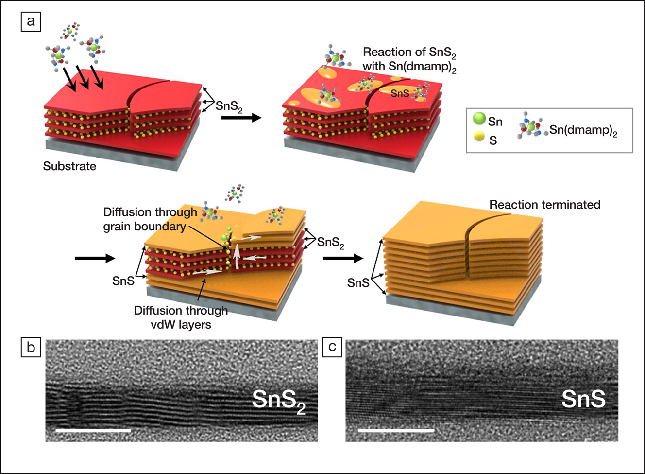
(a) The process of the transformation from SnS2 to SnS, where (dmamp)2 is bis(1-dimethylamino-2-methyl-2-propoxy)tin(II); transmission electron microscope images of (b) SnS2 and (c) SnS. Scale bars represent 10 nm. Credit: Chemistry of Materials.
Seong Keun Kim of the Korea Institute of Science and Technology, Republic of Korea, and co-workers have devised an in situ transformation as a new strategy to synthesize metal chalcogenides. They specifically demonstrated that exposing SnS2 nanosheets to the vapor of bis(1-dimethylamino-2-methyl-2-propoxy)tin(II) (Sn(dmamp)2) reduced SnS2 to SnS with a high purity yield. This finding has been published in Chemistry of Materials (doi: 10.1021/acs.chemmater.9b04387).
The SnS2-to-SnS transformation was accomplished using atomic layer deposition (ALD). ALD deposits thin films onto a substrate by stacking one atomic layer per reaction cycle. The researchers first grew a 4-nm-thick SnS2 film onto a SiO2 substrate, using Sn(dmamp)2 and H2S as the sources of Sn and S, respectively. Subsequently, H2S gas was eliminated, and they exposed the SnS2 thin film to only the vapor of Sn(dmamp)2 (1.06 Torr) at 270°C. In each reaction cycle, the exposure lasted for 2 s followed by purging for 10 s. After at least 200 cycles, the researchers confirmed that SnS2 was fully converted to SnS according to the lattice spacing measured by transmission electron microscopy, as well as a characteristic vibrational peak of SnS detected using Raman spectroscopy.
The discovery of this phase transformation occurred by serendipity. Kim, the corresponding author, says that the research team initially “… tried to fabricate vertical p–n junction diodes by stacking p-type SnS layers on n-type SnS2 layers using ALD.” However, instead of a double-layered SnS2/SnS heterostructure, they discovered that they had obtained a pure SnS thin film.
The mechanism of the transformation is associated with Sn2+ adsorption and S diffusion. Upon contacting SnS2, Sn(dmamp)2 adsorbed onto SnS2, and the dmamp ligands decomposed into volatile products, including acetone. The adsorbed Sn2+ then combined with the S atoms within the surface. With the reaction cycle repeated, the S atoms on the surface were mainly consumed, and those buried inside the SnS2 thin film started to diffuse upward to replenish the surface through grain boundaries. The transformation self-terminated once all the S atoms were reacted and, therefore, thoroughly converted SnS2 to SnS.
Yu Song of Northeastern University, China, whose research deals with two-dimensional (2D) metal dichalcogenides, says, “The in situ conversion strategy opens a new gate to the synthesis of continuous, high-quality, and large-area 2D metal chalcogenide thin films with tunable electronic and optical properties.” Song was not involved in this study.
Projecting forward, Kim says that his research team is developing strategies to address the challenge of thickness uniformity of the SnS films. “The polycrystalline SnS2 layer was adopted as the parent material to transform into SnS. The polycrystalline nature of the ALD-grown SnS2 layer inevitably results in nonuniformity in the thickness of the transformed SnS and generation of defects in the SnS layer,” Kim says. He envisions that this ALD-based conversion will be useful to synthesize a plethora of transition-metal chalcogenide pairs, including SnSe/SnSe2, BiTe/Bi2Te3, and Cu2S & CuS.
