


I. INTRODUCTION
FREQUENCY down conversion is a vital function in almost any microwave receiver. The simplest receivers are usually based on the homodyne or direct conversion architecture [Reference Razavi1]. This overcomes the problem with image frequency channel and leaves only the desired signal, directly at baseband. Mixers for direct conversion are also used in Doppler radars, as the direct conversion architecture gives the Doppler shift directly from the received frequency. Mixers for direct conversion have the drawback that the radio frequency (RF) and local oscillator (LO) frequencies are at the same frequency, thus good isolation between the ports is important as filtering is not possible. Also, as the output frequency is low, flicker or 1/f noise might be a problem.
The double balanced mixer ideally provides infinite isolation between all ports and is therefore a good choice to use as a mixer for direct conversion. Other benefits of the double balanced mixer are rejection of LO noise and high linearity [Reference Maas2]. The balancing circuits should, to get full benefit of the double balanced architecture, be well adjusted. This is challenging to achieve in practice due to process and manufacturing variances.
To utilize the broadband nature of the double balanced mixer, the balun should also be broadband otherwise the bandwidth of the mixer will be limited. The Marchand balun [Reference Marchand3] is in itself very broadband, and it is commonly used for this reason in a planar [Reference Zhang, Guo, Ong and Chia4–Reference Ma, Wang and Lai6] or lumped-distributed [Reference Ang, Leong and Lee7–Reference Miao, Zhang, Geng, Chen, Ma and Gao9] implementation. In [Reference Michaelsen, Johansen, Tamborg and Zhurbenko10] we presented a Marchand balun with tunable phase balance, and in [Reference Michaelsen, Johansen, Tamborg and Zhurbenko11, Reference Michaelsen, Johansen, Kjeld and Vitaliy12] we presented a broad band double balanced mixer using diode connected heterojunction bipolar transistors (HBTs) together with lumped Marchand baluns on RF and LO ports. The mixer design presented here integrates the tunable Marchand balun on the LO-port together with Schottky diodes for the mixing core. This allows to correct for any mismatches either in the balun design or in the mixing core itself. This should then enhance the benefits of practical implementations of double balanced mixers, where our focus will be on the properties important for direct conversion mixing, i.e. port isolation and linearity. To the author's knowledge a double balanced ring mixer with balance corrections using a tunable balun is demonstrated here for the first time.
II. DESIGN OF MIXER WITH TUNABLE BALUN
This section gives a description of the design of the circuitry. First a description of the lumped Marchand balun design with tunable phase balance is given. This will be followed by a description of the full mixer circuit. The theoretical treatment of the effect of LO balun imbalance on mixer characteristics can be found in Appendix V.
A) Marchand balun design
The broadband nature of the Marchand balun makes it an ideal candidate for a double balanced mixer. The idea of the tunable Marchand balun as described in [Reference Michaelsen, Johansen, Tamborg and Zhurbenko10] is to introduce a tunable shunt susceptance between the two coupled elements of the Marchand balun. The tuning range $\Delta \phi = \angle S_{21} - \angle S_{31}$
is given as [Reference Michaelsen, Johansen, Tamborg and Zhurbenko10]
$\Delta \phi = \angle S_{21} - \angle S_{31}$
is given as [Reference Michaelsen, Johansen, Tamborg and Zhurbenko10]
 $$\Delta \phi \approx \displaystyle{{Z_0(C^4 + C^2)} \over {C^2 + 1}}B_m,$$
where C is the coupling factor of the coupled line element, Z 0 is the characteristic impedance and B m = jωC m is the added susceptance.
A typical planar Marchand balun is realized using coupled transmission lines, and the introduction of a negative susceptance is difficult to synthesize. Instead the lumped element implementation [Reference Johansen and Krozer8] is suggested, as this already has a capacitance placed where the additional susceptance is required, allowing for an effective negative susceptance by having a smaller capacitance than normally required. The design procedure follows the one given in [Reference Johansen and Krozer8].
B) Mixer design
A diagram of the full mixer is shown in Fig. 1. The mixing core consists of four Schottky diodes in a ring, to enable the double balanced properties [Reference Maas2]. When choosing the diode size, the conversion-loss degradation factor [Reference Maas2] is a helpful guiding parameter
 $$\delta = 1 + \displaystyle{{R_s} \over {Z_s}} + \displaystyle{{Z_sf_{RF}^2} \over {R_sf_c^2}}, $$
where R
s
is the series resistance, Z
s
is the real diode junctions RF input resistance, and f
c
= 1/2πR
s
C
j
is the cutoff frequency. Increasing the diode area will decrease the series resistance, but increase the junction capacitance, C
j
, in such a manner that the cutoff frequency will decrease [Reference Rassel13]. But as the RF frequency is low compared to f
c
, a larger diode will give better conversion-loss degradation factor as the last term of (2) will be almost negligible. Using Harmonic Balance simulations a size was found such that using single series inductors, L
RF
and L
LO
for the RF and the LO ports, respectively, was sufficient to match to 50 Ω. This gave a diode area of 14.4(µm)2, with corresponding series resistance of R
s
= 19 Ω, junction capacitance of $C_{j_0} = 80\,{\rm fF}$
, which results in a cutoff frequency of f
c
= 105 GHz, and a loss degradation factor of δ = 1.5 dB.
$C_{j_0} = 80\,{\rm fF}$
, which results in a cutoff frequency of f
c
= 105 GHz, and a loss degradation factor of δ = 1.5 dB.
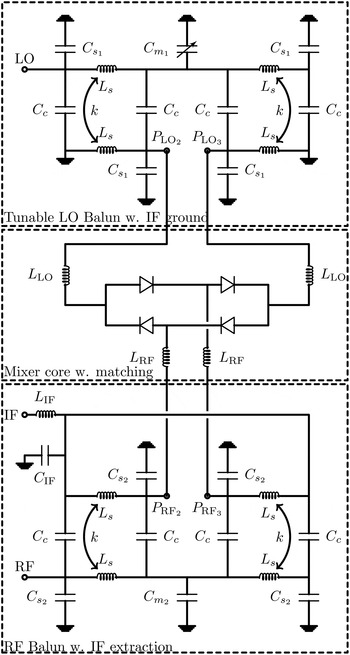
Fig. 1. Schematic of the double balanced mixer including RF and LO baluns.
The IF-extraction is similar to that described in [Reference Michaelsen, Johansen, Tamborg and Zhurbenko11]. That is, the RF balun has coupling capacitors C IF to its ground connection, allowing for the IF signal extraction. It is important to make the IF extraction symmetric as any asymmetry will affect the balun performance. On the LO side the balun will, by its grounding, ensure the IF-return path for the diode ring. Table 1 gives the design parameters.
Table 1. Design parameters for the mixer circuit.

C) Effect of tunable LO balun
In Appendix V the effect of LO balun imbalance on the performance of double balanced diode ring mixer is described theoretically. In particular, it is described how the DC offset, LO, and RF leakage, conversion loss, and second-order intermodulation depends upon an interaction between the LO balun imbalance (amplitude and phase imbalances) and load mismatch. The effect of load mismatch is described with a phenomenal parameter ΔZ. The load mismatch parameter is highly layout dependent and cannot be assessed a priori. Once the layout has been completed, however, it is possible to perform an electromagnetic (EM) simulation on the layout of the double balanced diode ring mixer circuit. This should provide a fair estimate of the effect of load mismatch. Figure 2 shows the 3D EM preview of the Schottky diode ring for the double balanced mixer using Momentum in ADS from Keysight Technologies. The interdigitated finger structure of the four Schottky diodes in the ring is clearly visual. Internal ports are provided at the internal anode and cathode connections of each Schottky diode. The EM result of the ring structure is subsequently included into the circuit schematic for Harmonic balance simulations. With this setup it is believed that the load mismatch caused by the asymmetry in the layout of the diode ring can be accurately predicted.
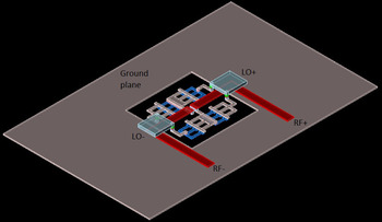
Fig. 2. 3D EM preview Schottky diode ring for the double balanced mixer using Momentum in ADS from Keysight Technologies.
According to the theoretical description in Appendix V the LO leakage at the IF port should not depend on the load mismatch. Therefore, we should expect the LO leakage to be minimized once the LO balun imbalance is minimized. Extending the above EM-circuit co-simulation approach to the complete mixer circuit including LO and RF baluns, matching inductors, and diode ring it is possible to predict the LO leakage as a function of phase difference between the complementary outputs of the LO balun. This is shown in Fig. 3 for an LO frequency of 11.5 GHz and LO power level of +11 dBm.

Fig. 3. LO leakage versus phase difference for the LO balun. The LO frequency is 11.5 GHz and the LO power is +11 dBm.
As expected from our theoretical description the LO leakage is minimized for a phase difference around 180° for the LO balun. The shown phase difference ranging from −184° to −176.5° corresponds to the achievable tuning range of the LO balun using the metal-oxide-semiconductor (MOS) varicap. The reason that the minimum of the LO leakage is not occurring exactly at 180° phase difference is that the LO balun also has a small amplitude imbalance. Despite this it is shown how even a rather limited tuning range can improve the LO leakage by approximately 7 dB. As described in Appendix V the second-order intermodulation is expected to depend simultaneously on interaction between the LO balun imbalance and the load mismatch. That is, no second-order intermodulation would be expected if either the LO balun imbalance or load mismatch are zero. Figure 4 shows the simulated second-order intermodulation product at the IF port. The LO frequency is set at 11.4 GHz and the LO power is set at +11 dBm. The two RF tones are at 11.5 and 11.513 GHz. Thus the second-order intermodulation project is at 13 MHz. The power in each of the two RF tones is –20 dBm. It is seen that tuning the phase balance of the LO balun indeed improves the second-order intermodulation product. Because the second-order intermodulation product depends on both the LO balun imbalance and the load mismatch the minimum is not reached at exactly a phase difference of 180°. Due to the presence of an amplitude imbalance the second-order intermodulation product cannot be cancelled completely.

Fig. 4. Second-order intermodulation product at IF port versus phase difference of the LO balun.
III. EXPERIMENTAL RESULTS
In this section the experimental results are discussed. The measurements are made on-wafer using a probe station, and calibration is used to remove losses in cables and probes.
The circuit is fabricated using a SiGe:C BiCMOS process from Innovations for High Performance Microelectronics (IHP). It is a 0.25 µm technology, but Schottky diodes are not a mature part of the process and may suffer from leakage current. Indeed, characterization of fabricated Schottky diodes revealed a significant leakage current with spreading across test sites. Their performance as mixer diodes, however, should not be affected too much by the leakage current. The process also has metal-insulator-metal (MIM) capacitors, MOS-varactors and five metal layers of which the upper two are extra thick, intended for passives or low loss interconnects.
First measurements of the Marchand balun, measured on a separate breakout, is presented in Section IIA) which is followed by a presentation of the measurements of the full mixer circuit in Section IIB).
A) Marchand balun experimental results
A break out of the circuit was manufactured, with a size of 700 µm × 990 µm, which is shown in Fig. 5. The matching capacitors, C s is implemented as MIM capacitors and variable capacitor, C m , is implemented using a MOS-varactor , which can be tuned from 0.35 to 1.0 pF. The inductors, L s , is implemented as broad-side coupled inductor pairs using the top two metal layers, for best Q-value. These are diagonally offset to get the desired inductive coupling, k, and capacitive coupling, C c .

Fig. 5. Microphotograph of the tunable Marchand balun, size 700 µm × 990 µm.
Figure 6 shows measurements of insertion loss, reflection, and isolation of the balun structure. The insertion loss is better than 7 dB on both channels in the range from 11 to 13 GHz, while having a return loss better than 14.5 dB. The magnitude balance is plotted in Fig. 7. At the center frequency of 12 GHz the magnitude balance can be tuned by 0.8 dB, from –0.8 to 0 dB. In Fig. 8 the phase difference is plotted for different bias values as a function of frequency. At the center frequency the phase difference can be tuned by 5.8°, from 171.6° to 177.4°, so a perfect match is not obtainable, but a large improvement of Δϕ is still possible.

Fig. 6. Insertion loss and input matching measured with tuning voltages ranging from –2.5 to 2.5 V.

Fig. 7. Measurement of magnitude imbalance with tuning voltages ranging from –2.5 to 2.5 V.

Fig. 8. Measurement of phase difference between output ports with tuning voltages ranging from –2.5 to 2.5 V.
B) Full mixer circuit
In this section, measurements of the combined mixer circuit are discussed. The circuit has a size of 2050 µm × 1000 µm, and in Fig. 9 is a microphotograph of the circuit. For all measurements the IF-frequency is 100 MHz.

Fig. 9. Microphotograph of the mixer circuit. Size 2050 µm × 1000 µm.
The conversion loss as a function of LO power at 11.5 GHz is plotted in Fig. 10, for measurements and simulation. It is almost saturated for a LO power level of 11 dBm with a conversion loss of 9.7 dB. Increasing the LO power level to 16 dBm will only give a small decrease in conversion loss to 9.3 dB. Thus for all other measurements the lower level of 11 dBm is chosen. A good agreement between measurement and simulation is observed, except when the diode is driven with low power. This is due to the diode model not being accurate at these power levels.

Fig. 10. Conversion loss as a function of LO power.
The conversion loss as a function of frequency is plotted in Fig. 11, for measurements and simulation. A good agreement between simulation and measurements is observed. A conversion loss of 8.8 dB is obtained at 11 GHz. The broadband nature of the Marchand balun is seen and the 3-dB bandwidth is from 8 to 13 GHz, covering the entire X-band and into the lower part of the Ku-band. It is seen that the conversion loss is independent of the bias voltage on the MOS varactor and thereby the LO balun imbalance. This trend is in agreement with the theoretical prediction using equation (A.25) in Appendix V.

Fig. 11. Conversion loss as a function of frequency.
Changing the tuning capacitance has a clear influence on the LO to IF isolation, as was predicted in equation (A.20) in Appendix V. At 11 GHz it can be changed from –41.3 dB at a bias voltage of –2.5 V to –48.7 dB at a bias voltage of 2.5 V. In Fig. 12 the LO to IF isolation is plotted as a function of balun tuning voltage for different frequencies. It is possible to reduce the isolation more for the higher frequencies, but this is what is expected as the phase balance of the balun is more sensitive to bias changes there and have better magnitude balance as shown in Figs 7 and 8.

Fig. 12. LO to IF isolation versus tuning voltage for different frequencies.
The RF–IF isolation is also constant, due to the fact that the main contributing mechanism to the leakage is unbalance in the RF-balun, which remains constant.
In Fig. 13 the DC offset is plotted versus the tuning voltage. It is possible to change the DC offset by a few mV, but there is a larger offset of around 9 mV, which cannot be completely removed. As would be expected there is a larger swing for the higher frequencies as the balun is more sensitive here. Apart from disturbing the following circuitry the DC offset is also unwanted as it increases the flicker noise level [Reference Michaelsen, Johansen and Tamborg14].

Fig. 13. DC level versus tuning voltage for different frequencies.
The linearity is plotted in Fig. 14. The 1 dB compression point is measured to be at 8 dBm RF input power.

Fig. 14. IF power versus RF power at the fundamental and second-order frequency for different tuning voltages. Extrapolated lines show IIP2.
Intermodulation is measured with two RF tones at frequencies of 11.5 and 11.513 GHz. For the measurements the second-order product at 13 MHz and the third-order product at 74 MHz is chosen . The LO frequency is 11.4 GHz. Isolators are placed after the signal generators to avoid leakage and intermodulation of the signals before they are applied to the mixer. Attenuation is added to the output of the mixer to avoid measuring the non-linearity of the spectrum analyzer [Reference Maas15]. From Fig. 14 the IIP2 can be read as the extrapolated values to be 45.5, 48.8 and 57.1 dBm for bias levels of –2.5, 0 and 2.5 V respectively, giving a 11.6 dB tuning range of IIP2. The curve corresponding to the 2.5 V bias point has a steeper slope for the last couple of points which could be a fourth-order phenomenon, as the one that was observed in [Reference Michaelsen, Johansen, Tamborg and Zhurbenko11]. The IIP3 is likewise found to be 20 dBm for all bias levels. This is according to the theory explained in Appendix V, where it was shown that the second-order intermodulation is sensitive to small changes in the balance, according to equation (A.26), whereas the third-order intermodulation is not, according to equation (A.28). Thus it is experimentally shown that a tunable balun can enhance the properties of the double balanced mixer, by increasing the LO–IF isolation and the IIP2.
In Table 2 the mixer is compared with other state-of-the-art direct conversion mixers reported in the open literature. As would be expected, from a SiGe technology, it is clear that if one wants an extremely linear circuit an active topology is not suitable. Of course, the active topology comes with the benefit of having 4.5 dB gain compared with −8.8 dB or worse for the passive diode-based topologies. The 1 dB compression point is lower than what is reported for [Reference Sudow, Andersson, Nilsson and Rorsman17] and [Reference Michaelsen, Johansen, Tamborg and Zhurbenko11], but these also exhibit more loss.
Table 2. Comparison between this work and recent reported direct conversion mixers.

The best IIP2 is achieved by [Reference Michaelsen, Johansen, Tamborg and Zhurbenko11], but after tuning our circuit is close to this and on par with [Reference Sudow, Andersson, Nilsson and Rorsman17].
An explanation for the poorer isolation and intermodulation is that a perfect balance is not obtained anywhere in the tuning range of the balun. For the mixer reported in [Reference Michaelsen, Johansen, Tamborg and Zhurbenko11] the inherent balun balance is believed to be extraordinary good which, however, can generally not be assured in all practical cases.
IV. CONCLUSION
We have presented a Schottky mixer design in a SiGe technology, with a balun, which is tunable to reduce leakage and enhance linearity. A breakout of the balun was measured. The full mixer has a size of 2050 µm× 1000 µm. The center frequency of the mixer is 11 GHz. Here it has a conversion loss of –8.8 dB with a LO power level of 11 dBm. The 3-dB bandwidth is from 8 to 13 GHz, more than the entire X-band. The conversion loss is constant over the tuning range. The LO–IF isolation on the other hand can change from 41.3 to 48.7 dBm at 11 GHz. The IIP2 can be improved by the tuning from 45.5 to 57.1 dBm, while the 1-dB compression point and IIP3 is kept constant at 6.7 and 20 dBm.
 Rasmus S. Michaelsen received the M.Sc. and Ph.D. degrees in Electrical Engineering from the Technical University of Denmark, Denmark, in 2010 and 2016, repectively. In 2009 he joined Weibel Scientific A/S, designing and testing X-band microwave components, and later as MMIC design engineer. In 2010 he was on an external stay at Physikalisches Institut, Johann Wolfgang Goethe-Universität, Frankfurt am Main, Germany. His current research interests include microwave monolithic integrated circuit (MMIC) design, nonlinear circuits, flicker noise and direct conversion receiver circuits.
 Tom K. Johansen received his M.S and Ph.D. degrees in Electrical Engineering from the Technical University of Denmark, Denmark, in 1999 and 2003, respectively. In 1999 he joined the Electromagnetic Systems group, DTU Elektro, Technical University of Denmark, Denmark, where he is currently an Associate Professor. From September 2001 to March 2002 he was a Visiting scholar at the center for wireless communication, University of San Diego, California, Ca. From November 2012 to February 2013 he spent a sabbatical at the Ferdinand Braun Institute (FBH), in Berlin, Germany. His research areas include the modeling of HBT devices, microwave, millimeter-wave, and sub-millimeter-wave integrated circuit design.
 Kjeld M. Tamborg was born in Kastrup, Denmark in 1966. He received his M.Sc. degree in Electronics from the Technical University of Denmark (DTU) in 1990. He was in 1990 hired by Weibel Scientific A/S, Allerød, Denmark, where he is still working. Since 2007 he has been responsible for the product Weibel radar antenna heads and components inside. During his work he has developed micro strip antenna elements, low noise amplifiers, power amplifiers, mixers, oscillators, and many other components for X-band radar.
 Vitaliy Zhurbenko received the M.Sc. degree from the Kharkiv National University of Radio Electronics in 2001, and the Ph.D. degree from the Technical University of Denmark in 2008, all in Electrical Engineering. From November 2000 to June 2005, he was a metrology engineer with the Laboratory of Metrology, Kharkiv, Ukraine. In 2005, he joined the Technical University of Denmark, where he is currently an Associate Professor. His current research interests include microwave and millimeter wave devices and integrated circuits for instrumentation applications; microwave and millimeter wave sensing for biomedical and security applications; microwave imaging and radars; antenna and passive circuit design and characterization.
 Lei Yan was born in Beijing, China, in 1980. He received the B.E. degree in Electronics Engineering from Xi'dian University, China, in 1998. He received the MSc. and Ph.D. degrees in Electrical Engineering department of Technical university of Denmark in 2007 and 2012, respectively. His previous research interests include wideband MMIC designs: low noise amplifiers, mixer, and mm-wave power amplifier. Since 2012, he joined the photonic-component department in Fraunhofer Heinrich-Hertz-Institut at Berlin for IC development in optical communication field.
APPENDIX
V. NON-IDEAL DOUBLE BALANCED MIXER THEORY
This section will give a theoretical description of the behavior of double balanced mixers in the case of non-ideal baluns. The main focus will be on DC offset, port isolation, and the intermodulation products. First we investigate the large signal conditions for the LO-voltage. This is followed by an analysis of the behavior of the ring mixer due to unbalance. The analysis takes the time-varying nature of the diodes non-linear conductances under the influence of LO balun imbalances into account. Thus it will be possible to identify the mechanisms responsible for DC offset, LO, and RF leakage, conversion loss, and second-order intermodulation products.
The diode ring, which will be used as the core of the double balanced mixer is depicted in Fig. 15. The current through each Schottky diode is given by
 $$I_{d_n} = I_s\left( {\exp \left( {\displaystyle{{V_{d_n}} \over {\eta V_T}}} \right) - 1} \right),$$
where I
s
is the saturation current, $V_{d_n}$
is the large signal diode voltage across diode n, η is the ideality factor and V
T
is the thermal voltage.
$V_{d_n}$
is the large signal diode voltage across diode n, η is the ideality factor and V
T
is the thermal voltage.

Fig. 15. Schottky diode ring.
To find the LO-voltage across a single diode in the diode ring, we look at the left and right half-circuit independently. The half-circuit is shown in Fig. 16, where the impedance Z m is a combination of IF, RF load, and embedding network. Using the definitions on the figure, we have the following voltage relation:
 $$V_a = V_{d_1} + Z_mI_m, $$
 $$V_b = - V_{d_2} + Z_mI_m,$$
 $${\rm where}\;I_m = i_a + i_b = I_s\left( {\exp \left( {\displaystyle{{V_{d_1}} \over {\eta V_T}}} \right) - \exp \left( {\displaystyle{{V_{d_2}} \over {\eta V_T}}} \right)} \right).$$
The signals V a and V b can be given as
 $$V_a = V_{LO}\left( {1 - \displaystyle{{\Delta A} \over 2}} \right)\cos \left( {\omega _{LO}t - \displaystyle{{\Delta \phi} \over 2}} \right),$$
 $$V_b = - V_{LO}\left( {1 + \displaystyle{{\Delta A} \over 2}} \right)\cos \left( {\omega _{LO}t + \displaystyle{{\Delta \phi} \over 2}} \right),$$
where we have introduced a phase error, Δϕ, and a amplitude error ΔA. This allows us to investigate the consequences of imbalance on circuit performance. We also introduce a load imbalance on the IF load given as $Z_{m_{left}} = Z_m(1 + (\Delta Z/2))$
and
$Z_{m_{left}} = Z_m(1 + (\Delta Z/2))$
and $Z_{m_{right}} = Z_m (1 - (\Delta Z/2))$
for the left and right half circuits, respectively. The term Z
m
Im
from (A.2), which will contribute to a voltage difference across the two diodes, is approximated by the term
$Z_{m_{right}} = Z_m (1 - (\Delta Z/2))$
for the left and right half circuits, respectively. The term Z
m
Im
from (A.2), which will contribute to a voltage difference across the two diodes, is approximated by the term $(1 \pm A_Z(1 - (\Delta Z/2)))$
, where A
Z
is a function of the amplitude and phase balance. This term reduces to zero if the amplitude and phase balance are both zero. Then the large signal diode voltages can be approximated to
$(1 \pm A_Z(1 - (\Delta Z/2)))$
, where A
Z
is a function of the amplitude and phase balance. This term reduces to zero if the amplitude and phase balance are both zero. Then the large signal diode voltages can be approximated to
 $$\eqalign{V_{d_1} = V_{LO}\left( {1 - \displaystyle{{\Delta A} \over 2}} \right)\cos \left( {\omega _{LO}t - \displaystyle{{\Delta \phi} \over 2}} \right)\left( {1 - A_Z\left( {1 + \displaystyle{{\Delta Z} \over 2}} \right)} \right),}$$
 $$\eqalign{V_{d_2} = V_{LO}\left( {1 + \displaystyle{{\Delta A} \over 2}} \right)\cos \left( {\omega _{LO}t + \displaystyle{{\Delta \phi} \over 2}} \right)\left( {1 + A_Z\left( {1 + \displaystyle{{\Delta Z} \over 2}} \right)} \right),}$$
 $$\eqalign{V_{d_3} = - V_{LO}\left( {1 + \displaystyle{{\Delta A} \over 2}} \right)\cos \left( {\omega _{LO}t + \displaystyle{{\Delta \phi} \over 2}} \right)\left( {1 + A_Z\left( {1 - \displaystyle{{\Delta Z} \over 2}} \right)} \right),}$$
 $$\eqalign{V_{d_4} = - V_{LO}\left( {1 - \displaystyle{{\Delta A} \over 2}} \right)\cos \left( {\omega _{LO}t - \displaystyle{{\Delta \phi} \over 2}} \right)\left( {1 - A_Z\left( {1 - \displaystyle{{\Delta Z} \over 2}} \right)} \right).}$$
From Fig. 15 we have
 $$I_{\rm 1} = I_{d_1} - I_{d_2},$$
 $$I_{\rm 2} = I_{d_3} - I_{d_4}.$$
Summing these gives the currents at the IF port and the difference gives the current at the RF port
 $$I_{{\rm IF}} = I_{\rm 1} + I_{\rm 2},$$
 $$I_{RF} = I_1 - I_2.$$
The current through each diode as a function of RF voltage can be expressed as a Taylor series taken around the large signal LO voltage
 $$\eqalign{I_{d_n}(t) = I_{0_{d_n}}(t) + g_{1_{d_n}}(t)v + g_{2_{d_n}}(t)v^2 + g_{3_{d_n}}(t)v^3 + \cdots,}$$
where d
n
denotes the diode number n, $I_{0_{d_n}} = I_d(V)\vert_{V = V_{d_n}}$
,
$I_{0_{d_n}} = I_d(V)\vert_{V = V_{d_n}}$
, $g_1 = \left. {dI_d(V)/dV} \right\vert_{V = V_{d_n}}$
, and
$g_1 = \left. {dI_d(V)/dV} \right\vert_{V = V_{d_n}}$
, and $g_2 = 1/2\left. {d^2I_d(V)/dV^2} \right\vert_{V = V_{d_n}}$
.
$g_2 = 1/2\left. {d^2I_d(V)/dV^2} \right\vert_{V = V_{d_n}}$
.

Fig. 16. Half circuit of diode ring, left side.
Using (A.12) we will investigate how the DC offset, LO, and RF leakage, conversion loss and second-order intermodulation depends on the unbalances. For each diode the current will be given as
 $$I_{d_1} = I_{0_{d_1}}(t) - g_{1_{d_1}}(t)v_{RF} + g_{2_{d_1}}(t)v_{RF}^2 - g_{3_{d_1}}(t)v_{RF}^3,$$
 $$I_{d_2} = I_{0_{d_2}}(t) + g_{1_{d_2}}(t)v_{RF} + g_{2_{d_2}}(t)v_{RF}^2 + g_{3_{d_2}}(t)v_{RF}^3,$$
 $$I_{d_3} = I_{0_{d_3}}(t) + g_{1_{d_3}}(t)v_{RF} + g_{2_{d_3}}(t)v_{RF}^2 + g_{3_{d_3}}(t)v_{RF}^3,$$
 $$I_{d_4} = I_{0_{d_4}}(t) - g_{1_{d_4}}(t)v_{RF} + g_{2_{d_4}}(t)v_{RF}^2 - g_{3_{d_1}}(t)v_{RF}^3.$$
A) DC offset from LO drive
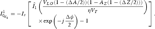
From (A.12) a DC contribution comes from the first term I 0(t) or the even ordered terms, for ω LO ≠ ω RF . In this section we will only look at the DC that comes from the I 0(t) term, in Section VE) we look at the DC term coming from higher orders. It should be mentioned that other mechanisms can also add to the DC offset, such as LO-self mixing due to a parasitic path from the LO port to the RF port before the mixer core [Reference Michaelsen, Johansen and Tamborg14]. The zero-order Fourier coefficient corresponds to the DC-current through each diode. The zero-order Fourier coefficient I 0(t) corresponds to the DC-current through each diode can be found as [Reference Michaelsen, Johansen and Krozer18]
 $$I_{0_{d_1}}^0 = I_s\left[ {{\hat I}_0\left( {\displaystyle{{V_{LO}(1 - (\Delta A/2))(1 - A_Z(1 + (\Delta Z/2)))} \over {\eta V_T}}} \right) - 1} \right],$$
 $$I_{0_{d_2}}^0 = I_s\left[ {{\hat I}_0\left( {\displaystyle{{V_{LO}(1 + (\Delta A/2))(1 + A_Z(1 + (\Delta Z/2)))} \over {\eta V_T}}} \right) - 1} \right],$$
 $$I_{0_{d_3}}^0 = I_s\left[ {{\hat I}_0\left( {\displaystyle{{V_{{\rm LO}}(1 + (\Delta A/2))(1 + A_Z(1 - (\Delta Z/2)))} \over {\eta V_T}}} \right) - 1} \right],$$
 $$I_{0_{d_4}}^0 = I_s\left[ {{\hat I}_0\left( {\displaystyle{{V_{LO}(1 - (\Delta A/2))(1 - A_Z(1 - (\Delta Z/2)))} \over {\eta V_T}}} \right) - 1} \right],$$
where $\hat I_0(x)$
is the modified Bessel function of order 0 and argument x. As the deviations are all small, linearizing will give better insight. First we reformulate the nominator in (A.14a)
$\hat I_0(x)$
is the modified Bessel function of order 0 and argument x. As the deviations are all small, linearizing will give better insight. First we reformulate the nominator in (A.14a)
 $$V_{LO}\left( {1 - \displaystyle{{\Delta A} \over 2}} \right)\left( {1 - A_Z\left( {1 - \displaystyle{{\Delta Z} \over 2}} \right)} \right) = V_{LO}\left( {1 + a} \right),$$
where $a = - \Delta A/2 - A_Z(1 - (\Delta Z/2)) + \Delta A/(2)A_Z(1 - (\Delta Z/2))$
. Similar relations can be formulated for (A.15) through (A.14d). Then linearizing the Bessel function around V
LO
, for small deviations of a, using [9.6.28] in [Reference Abramowitz and Stegun19], gives
$a = - \Delta A/2 - A_Z(1 - (\Delta Z/2)) + \Delta A/(2)A_Z(1 - (\Delta Z/2))$
. Similar relations can be formulated for (A.15) through (A.14d). Then linearizing the Bessel function around V
LO
, for small deviations of a, using [9.6.28] in [Reference Abramowitz and Stegun19], gives
 $$\hat I_0\left( {\displaystyle{{V_{LO}(1 + a)} \over {\eta V_T}}} \right) = \hat I_0\left( {\displaystyle{{V_{LO}} \over {\eta V_T}}} \right) + \displaystyle{{V_{LO}} \over {\eta V_T}}\hat I_1\left( {\displaystyle{{V_{LO}} \over {\eta V_T}}} \right)a,$$
where $\hat I_1(x)$
is the modified Bessel function of first order and argument x. Using this relation in (A.14a) through (A.14d), inserting them into (A.8) and (A.9), and then into (A.10) we get
$\hat I_1(x)$
is the modified Bessel function of first order and argument x. Using this relation in (A.14a) through (A.14d), inserting them into (A.8) and (A.9), and then into (A.10) we get
 $$\eqalign{I_{IF} &= I_{0_{d_1}}^0 - I_{0_{d_2}}^0 + I_{0_{d_3}}^0 - I_{0_{d_4}}^0 \cr &= - I_s\displaystyle{{V_{LO}} \over {\eta V_T}}{\hat I}_1\left( {\displaystyle{{V_{LO}} \over {\eta V_T}}} \right)4A_Z\displaystyle{{\Delta Z} \over 2}.}$$
This shows that a DC contribution comes directly from the LO signal in the mixer core due to load mismatch (ΔZ) together with LO balun imbalance (contained in A Z ). For a properly designed circuit this contribution to the DC offset should be of a little concern.
B) LO leakage
The LO leakage is found as the fundamental current running through the diodes to the IF port, corresponding to the first-order term of the Fourier series of $I_{0d_n}$
. The first-order Fourier coefficients of
$I_{0d_n}$
. The first-order Fourier coefficients of $I_{0d_n}$
can be found as [Reference Michaelsen, Johansen and Krozer18]
$I_{0d_n}$
can be found as [Reference Michaelsen, Johansen and Krozer18]
 $$I_{0_{d_1}}^1 = I_s\left[ \matrix{{\hat I}_1\left( {\displaystyle{{V_{LO}(1 - (\Delta A/2))(1 - A_Z(1 + (\Delta Z/2)))} \over {\eta V_T}}} \right) \hfill \cr \quad \times \exp \left( { - j\displaystyle{{\Delta \phi } \over 2}} \right) - 1 \hfill} \right],$$
 $$I_{0_{d_2}}^1 = I_s\left[ \matrix{{\hat I}_1\left( {\displaystyle{{V_{LO}(1 + (\Delta A/2))(1 + A_Z(1 + (\Delta Z/2)))} \over {\eta V_T}}} \right) \hfill \cr \quad \times \exp \left( {j\displaystyle{{\Delta \phi } \over 2}} \right) - 1 \hfill} \right],$$
 $$I_{0_{d_3}}^1 = - I_s\left[ \matrix{{\hat I}_1\left( {\displaystyle{{V_{LO}(1 + (\Delta A/2))(1 + A_Z(1 - (\Delta Z/2)))} \over {\eta V_T}}} \right) \hfill \cr \quad \times \exp \left( {j\displaystyle{{\Delta \phi } \over 2}} \right) - 1 \hfill} \right],$$
 $$I_{0_{d_4}}^1 = - I_s\left[ \matrix{{\hat I}_1\left( {\displaystyle{{V_{LO}(1 - (\Delta A/2))(1 - A_Z(1 - (\Delta Z/2)))} \over {\eta V_T}}} \right) \hfill \cr \quad \times \exp \left( { - j\displaystyle{{\Delta \phi } \over 2}} \right) - 1 \hfill} \right].$$
The term $\exp (j(\Delta \phi /2))$
is due to the phase mismatch, because when calculating the n’th Fourier coefficient this appears as the modified Bessel function times a factor
$\exp (j(\Delta \phi /2))$
is due to the phase mismatch, because when calculating the n’th Fourier coefficient this appears as the modified Bessel function times a factor $\exp \left( {jn(\Delta \phi /2)} \right)$
[Reference Michaelsen, Johansen and Krozer18]. Linearizing the modified Bessel function of first order around V
LO
, that is for small deviations, using [9.6.28] in [Reference Abramowitz and Stegun19], gives
$\exp \left( {jn(\Delta \phi /2)} \right)$
[Reference Michaelsen, Johansen and Krozer18]. Linearizing the modified Bessel function of first order around V
LO
, that is for small deviations, using [9.6.28] in [Reference Abramowitz and Stegun19], gives
 $$\eqalign{{\hat I}_1\left( {\displaystyle{{V_{LO}(1 + a)} \over {\eta V_T}}} \right) &= {\hat I}_1\left( {\displaystyle{{V_{LO}} \over {\eta V_T}}} \right) + \displaystyle{1 \over 2}\displaystyle{{V_{LO}} \over {\eta V_T}} \cr & \quad \times \left( {{\hat I}_0\left( {\displaystyle{{V_{LO}} \over {\eta V_T}}} \right) + {\hat I}_2\left( {\displaystyle{{V_{LO}} \over {\eta V_T}}} \right)} \right)a.}$$
Using this relation in (A.14a) through (A.14d), inserting them into (A.8) and (A.9), and then into (A.10) we get
 $$\eqalign{I_{IF} = & - 2jI_s\displaystyle{{V_{LO}} \over {\eta V_T}}\left( {{\hat I}_0\left( {\displaystyle{{V_{LO}} \over {\eta V_T}}} \right) + {\hat I}_2\left( {\displaystyle{{V_{LO}} \over {\eta V_T}}} \right)} \right) \cr & \quad \times \left[ {\cos \left( {\displaystyle{{\Delta \phi} \over 2}} \right)\left( {A_Z + \displaystyle{{\Delta A} \over 2}} \right) + j\sin \left( {\displaystyle{{\Delta \phi} \over 2}} \right)\displaystyle{{\Delta A} \over 2}A_Z} \right].}$$
From (A.20) it is seen that there is a strong connection between balun imbalances and the LO leakage, but no dependence on load mismatch.
C) RF leakage
The second term of (A.12) describes the linear behavior of the RF current. The RF leakage is found as the zeroth-order Fourier coefficient of $g_{1_{d_n}}(t)$
. This can be evaluated as [Reference Michaelsen, Johansen and Krozer18]
$g_{1_{d_n}}(t)$
. This can be evaluated as [Reference Michaelsen, Johansen and Krozer18]
 $$G_{1_{d_1}}^0 = \displaystyle{{I_s} \over {\eta V_T}}\hat I_0\left( {\displaystyle{{V_{LO}(1 - (\Delta A/2))(1 - A_Z(1 + (\Delta Z/2)))} \over {\eta V_T}}} \right),$$
 $$G_{1_{d_2}}^0 = \displaystyle{{I_s} \over {\eta V_T}}\hat I_0\left( {\displaystyle{{V_{LO}(1 + (\Delta A/2))(1 + A_Z(1 + (\Delta Z/2)))} \over {\eta V_T}}} \right),$$
 $$G_{1_{d_3}}^0 = \displaystyle{{I_s} \over {\eta V_T}}\hat I_0\left( {\displaystyle{{V_{LO}(1 + (\Delta A/2))(1 + A_Z\left( {1 - (\Delta Z/2)} \right))} \over {\eta V_T}}} \right),$$
 $$G_{1_{d_4}}^0 = \displaystyle{{I_s} \over {\eta V_T}}\hat I_0\left( {\displaystyle{{V_{LO}(1 - (\Delta A/2))(1 - A_Z(1 - (\Delta Z/2)))} \over {\eta V_T}}} \right).$$
Linearizing the Bessel function and using equations (A.13) through (A.14) we get
 $$\eqalign{I_{IF} &= ( - G_{1_{d_1}}^0 - G_{1_{d_2}}^0 + G_{1_{d_3}}^0 + G_{1_{d_4}}^0 )v_{RF} \cr &= - 4v_{RF}\displaystyle{{I_sV_{LO}} \over {{(\eta V_T)}^2}}{\hat I}_1\left( {\displaystyle{{V_{LO}} \over {\eta V_T}}} \right)\displaystyle{{\Delta A} \over 2}A_Z\displaystyle{{\Delta Z} \over 2}.}$$
As observed from (A.22), an imbalance in the LO balun will result in a RF leakage if there is also simultaneously a mismatch in the IF-load. This is not to say that this is the only way a RF-leak can occur, an imbalance in the RF-balun has a high impact on the RF-leakage, but this is outside the scope of this analysis.
D) Conversion loss
The desired mixing product at the IF frequency is found when the RF signal is multiplied with the fundamental tone of $g_{1_{d_n}}(t)$
. The contribution can be evaluated from the first-order Fourier coefficients as
$g_{1_{d_n}}(t)$
. The contribution can be evaluated from the first-order Fourier coefficients as
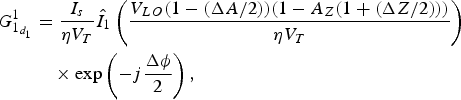 $$\eqalign{ G_{1_{d_1}}^1 &= \displaystyle{{I_s} \over {\eta V_T}}{\hat I}_1\left( {\displaystyle{{V_{LO}(1 - (\Delta A/2))(1 - A_Z(1 + (\Delta Z/2)))} \over {\eta V_T}}} \right) \cr & \quad \times \exp \left( { - j\displaystyle{{\Delta \phi } \over 2}} \right),}$$
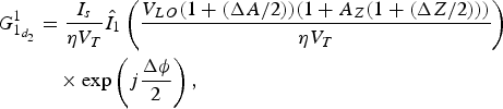 $$\eqalign{ G_{1_{d_2}}^1 &= \displaystyle{{I_s} \over {\eta V_T}}{\hat I}_1\left( {\displaystyle{{V_{LO}(1 + (\Delta A/2))(1 + A_Z(1 + (\Delta Z/2)))} \over {\eta V_T}}} \right) \cr & \quad \times \exp \left( {j\displaystyle{{\Delta \phi } \over 2}} \right),}$$
 $$G_{1_{d_3}}^1 = - \displaystyle{{I_s} \over {\eta V_T}}\hat I_1\left( {\displaystyle{{V_{LO}(1 + (\Delta A/2))(1 + A_Z(1 - (\Delta Z/2)))} \over {\eta V_T}}} \right) \times \exp \left( {j\displaystyle{{\Delta \phi } \over 2}} \right),$$
 $$\eqalign{ G_{1_{d_4}}^1 &= - \displaystyle{{I_s} \over {\eta V_T}}{\hat I}_1\left( {\displaystyle{{V_{LO}(1 - (\Delta A/2))(1 - A_Z(1 - (\Delta Z/2)))} \over {\eta V_T}}} \right) \cr & \quad \times \exp \left( { - j\displaystyle{{\Delta \phi } \over 2}} \right).}$$
Linearizing the Bessel function and using equations (A.13) through (A.14) we get
 $$\eqalign{I_{IF} &= ( - G_{1_{d_1}}^1 - G_{1_{d_2}}^1 + G_{1_{d_3}}^1 + G_{1_{d_4}}^1 )v_{RF} \cr &= - 4v_{RF}\displaystyle{{I_s} \over {\eta V_T}}\left[ {{\hat I}_1\left( {\displaystyle{{V_{LO}} \over {\eta V_T}}} \right)\cos \left( {\displaystyle{{\Delta \phi} \over 2}} \right)} \right. \cr & \quad + \displaystyle{1 \over 2}\displaystyle{{V_{LO}} \over {\eta V_T}}\left( {{\hat I}_2\left( {\displaystyle{{V_{LO}} \over {\eta V_T}}} \right) + {\hat I}_0\left( {\displaystyle{{V_{LO}} \over {\eta V_T}}} \right)} \right) \cr & \quad \times \left. {\left( {A_Z\displaystyle{{\Delta A} \over 2}\cos \left( {\displaystyle{{\Delta \phi} \over 2}} \right) + j\left( {A_Z + \displaystyle{{\Delta A} \over 2}} \right)\sin \left( {\displaystyle{{\Delta \phi} \over 2}} \right)} \right)} \right].}$$
The conversion loss is inversely proportional to the IF current. Therefore, it is observed that the conversion loss is not affected much by the phase imbalance as $\cos (\Delta \phi /2) \approx 1$
and the second term is negligible under the assumption of small deviations.
$\cos (\Delta \phi /2) \approx 1$
and the second term is negligible under the assumption of small deviations.
E) Second-order intermodulation
The third term of (A.12) describes the second-order behavior of the RF current. The zeroth-order Fourier coefficient of $g_{2_{d_n}}(t)$
, gives rise to the second-order intermodulation and DC-contribution from the RF signal. The Fourier coefficient can be found as [Reference Michaelsen, Johansen and Krozer18]
$g_{2_{d_n}}(t)$
, gives rise to the second-order intermodulation and DC-contribution from the RF signal. The Fourier coefficient can be found as [Reference Michaelsen, Johansen and Krozer18]
 $$\eqalign{G_{2_{d_1}}^0 \!\!\!= \displaystyle{{I_s} \over {2{(\eta V_T)}^2}} \times \hat I_0\left( {\displaystyle{{V_{LO}(1 - (\Delta A/2))(1 - A_Z(1 + (\Delta Z/2)))} \over {\eta V_T}}} \right),}$$
 $$\eqalign{G_{2_{d_2}}^0 \!\!\!\!= \displaystyle{{I_s} \over {2{(\eta V_T)}^2}} \times \hat I_0\left( {\displaystyle{{V_{LO}(1 + (\Delta A/2))(1 + A_Z(1 + (\Delta Z/2)))} \over {\eta V_T}}} \right),}$$
 $$\eqalign{G_{2_{d_3}}^0 \!\!\!\!= \displaystyle{{I_s} \over {2{(\eta V_T)}^2}} \times \hat I_0\left( {\displaystyle{{V_{{\rm LO}}(1 + (\Delta A/2))(1 + A_Z(1 - (\Delta Z/2)))} \over {\eta V_T}}} \right),}$$
 $$\eqalign{G_{2_{d_4}}^0 \!\!\!\!= \displaystyle{{I_s} \over {2{(\eta V_T)}^2}} \times \hat I_0\left( {\displaystyle{{V_{{\rm LO}}(1 - (\Delta A/2))(1 - A_Z(1 - (\Delta Z/2)))} \over {\eta V_T}}} \right).}$$
Again by linearizing the Bessel function and using equations (A.13) through (A.14) we get
 $$\eqalign{I_{IF} &= \left( {G_{2_{d_1}}^0 - G_{2_{d_2}}^0 + G_{2_{d_3}}^0 - G_{2_{d_4}}^0} \right)v_{RF}^2 \cr &= - 2\displaystyle{{V_{LO}I_s} \over {{(\eta V_T)}^3}}{\hat I}_1\left( {\displaystyle{{V_{LO}} \over {\eta V_T}}} \right)A_Z\displaystyle{{\Delta Z} \over 2}v_{RF}^2.}$$
From (A.26) we see that second-order intermodulation products will arise if there is a load mismatch together with a LO-balun imbalance.
F) Third-order intermodulation
The fourth term of (A.12) describes the third-order behavior of the RF current. To mix the frequencies to be near the IF frequency, it is neccessary for the third-order RF to mix with the LO, i.e. it is the first-order Fourier coefficient of $g_{2_{d_n}}(t)$
, which give rise to the third-order intermodulation from the RF signal. The Fourier coefficient can be found as [Reference Michaelsen, Johansen and Krozer18]
$g_{2_{d_n}}(t)$
, which give rise to the third-order intermodulation from the RF signal. The Fourier coefficient can be found as [Reference Michaelsen, Johansen and Krozer18]
 $$G_{3_{d_1}}^1 = \displaystyle{{I_s} \over {6{(\eta V_T)}^3}}\hat I_1\left( {\displaystyle{{V_{LO}(1 - (\Delta A/2))(1 - A_Z(1 + (\Delta Z/2)))} \over {\eta V_T}}} \right)\exp \left( { - j\displaystyle{{\Delta \phi} \over 2}} \right),$$
 $$G_{3_{d_2}}^1 = \displaystyle{{I_s} \over {6{(\eta V_T)}^3}}\hat I_1\left( {\displaystyle{{V_{LO}(1 + (\Delta A/2))(1 + A_Z(1 + (\Delta Z/2)))} \over {\eta V_T}}} \right)\exp \left( {j\displaystyle{{\Delta \phi} \over 2}} \right),$$
 $$G_{3_{d_3}}^1 = - \displaystyle{I_s \over 6(\eta V_T)^3} \hat{I}_1\left(\displaystyle{V_{LO}(1 + (\Delta A/2))(1 + A_Z(1 - (\Delta Z/2))) \over \eta V_T} \right)\exp \left(j\displaystyle{\Delta \phi \over 2} \right),$$
 $$G_{3_{d_4}}^1 = - \displaystyle{{I_s} \over {6{(\eta V_T)}^3}}\hat I_1\left( {\displaystyle{{V_{LO}(1 - (\Delta A/2))(1 - A_Z(1 - (\Delta Z/2)))} \over {\eta V_T}}} \right)\exp \left( { - j\displaystyle{{\Delta \phi} \over 2}} \right).$$
Linearizing the Bessel function and using equations (A.13) through (A.14) we get
 $$\eqalign{I_{IF} &= \Big( - G_{3_{d_1}}^1 - G_{3_{d_2}}^1 + G_{3_{d_3}}^1 + G_{3_{d_4}}^1 \Big)v_{RF}^3 \cr & = - \displaystyle{2 \over 3}v_{RF}\displaystyle{{I_s} \over {{(\eta V_T)}^3}}\left[ \matrix{{\hat I}_1\left( {\displaystyle{{V_{LO}} \over {\eta V_T}}} \right)\cos \left( {\displaystyle{{\Delta \phi } \over 2}} \right) + \displaystyle{1 \over 2}\displaystyle{{V_{LO}} \over {\eta V_T}} \hfill \cr \left( {{\hat I}_2\left( {\displaystyle{{V_{LO}} \over {\eta V_T}}} \right) + {\hat I}_0\left( {\displaystyle{{V_{LO}} \over {\eta V_T}}} \right)} \right) \hfill} \right. \cr & \quad \times \left. {\left( {A_Z\displaystyle{{\Delta A} \over 2}\cos \left( {\displaystyle{{\Delta \phi } \over 2}} \right) + j\left( {A_Z + \displaystyle{{\Delta A} \over 2}} \right)\sin \left( {\displaystyle{{\Delta \phi } \over 2}} \right)} \right)} \right].}$$
It is observed that the third-order intermodulation is not affected much by the phase imbalance as $\cos (\Delta \phi /2) \approx 1$
and the second term is negligible under the assumption of small deviations, just like the conversion loss.
$\cos (\Delta \phi /2) \approx 1$
and the second term is negligible under the assumption of small deviations, just like the conversion loss.


