


1. Introduction
Device quality InGaN films have led to the development of LEDs and blue laser diodes (LDs) by Nichia Chemical Industries, Ltd. Reference Nakamura, Senoh, Iwasa, Nagahama, Yamada and Mukai[1] Reference Nakamura, Senoh, Nagahama, Iwasa, Yamada, Matsushita, Kiyoku and Sugimoto[2] Thus, the use of III-nitrides as commercially viable devices has been proven. These achievements not withstanding, the growth of InGaN is hindered by several difficulties. They include:
-
1. The weak In-N bond necessitating the use of a high equilibrium vapor pressure of nitrogen to prevent In-N dissociation. The vapor pressure of nitrogen over InN is several orders of magnitude higher than that of AlN and GaN. Reference Matsuoka, Tanaka, Sasaki and Katsui[3]
-
2. Gas phase reactions between organometallics (OMs) and hydride precursors deteriorate the quality of In-based alloys.
-
3. The large lattice mismatch between AlGaN and InGaN. This is a problem since devices utilize the AlGaN/InGaN heterostructure. To avoid this, a well thickness of about 20 Å has been used. Reference Nakamura, Senoh, Iwasa, Nagahama, Yamada and Mukai[1] Thus, in order to increase the InN% in the active layer, using an AlGaN barrier layer imposes limitations on the range of heterostructures that can be grown. This can be avoided if the AlGaN layer is replaced by the more versatile AlInGaN alloy since the bandgap and lattice constant can be independently varied to achieve AlInGaN/InGaN lattice-matched structures.
The AlInGaN alloy has only recently began receiving serious attention into its growth and application. We have reported Reference McIntosh, Boutros, Roberts, Bedair, Piner and El-Masry[4] on the deposition of AlInGaN bulk films by MOCVD. The major difficulty in developing the III-nitride compound quaternary is determining the optimum growth temperature. Aluminum based compounds generally require higher growth temperatures to obtain reasonable crystal quality. Lower temperatures are required, however, for indium based compounds due to the difficulties mentioned earlier. The growth temperature will therefore limit the extent to which both In and Al can be incorporated into the AlInGaN compound.
This paper will discuss the growth of InGaN and AlInGaN alloys with up to 40% InN in bulk ternaries and an apparent 65% in thin films, and quaternaries with up to 20% AlN and 20% InN using a modified atmospheric pressure MOCVD reactor. Room temperature photoluminescence (PL) is dominated by band edge emission for InGaN and AlInGaN with low AlN%. Higher AlN% in AlInGaN show PL dominated by deep levels. AlInGaN/InGaN and AlGaN/InGaN heterostructures have been grown with abrupt interfaces observed by cross-sectional TEM and sharp, apparently band edge emission by room temperature PL. We emphasize the most important parameters for the growth of In-based thin films.
2. Experiment
A versatile reactor has been designed for III-nitride growth based on a rotating susceptor and has been described elsewhere. Reference Boutros, McIntosh, Roberts, Bedair, Piner and El-Masry[5] Reference Karam, Parodos, Colter, McNulty, Rowland, Schetzina, El-Masry and Bedair[6] The versatility of the system is due to its unique susceptor design, shown in Figure 1, allowing the system to operate in three different growth modes: MOCVD, molecular stream epitaxy (MSE), and atomic layer epitaxy (ALE). For MOCVD and MSE, ammonia is injected through ‘Port 2’ with ‘Port 3’ flowing nitrogen. For MOCVD, the ‘Rotating susceptor’, which holds the sample, remains stationary under the OMs/ammonia flow during the entire growth. For MSE the ‘Rotating susceptor’ rotates intermittently exposing the sample to the OM/ammonia stream. This allows a thin layer of material to be deposited and effectively annealed during each rotation cycle. For ALE growth, nitrogen is injected through ‘Port 2’ and ammonia through ‘Port 3’ thus separating the reactant gases and eliminating gas phase reactions. The sample is first exposed to the OM gas stream and then rotated under the ammonia gas stream. When the sample returns to the OM gas stream one cycle is complete.

Figure 1. Rotating susceptor design for the growth of III-nitride
Source gases used were trimethylaluminum (TMAl, +18°C), trimethylgallium (TMGa, −10°C), ethyldimethylindium (EDMIn, +10°C) and ammonia. Purified nitrogen was used as the carrier gas. (0001) sapphire, cleaved into approximately 1.5 cm by 1.5 cm squares, was used as the substrate. After solvent cleaning, the substrate was loaded, then annealed under nitrogen for 15 minutes followed by passivation under ammonia for 1 minute both at 1050°C. For the growth of bulk AlInGaN, an AlN buffer layer and then a GaN buffer layer each approximately 400 Å thick were grown at 900°C Reference Piner, He, Boutros, McIntosh, Roberts, Bedair and El-Masry[7] using the MSE growth technique. For the growth of bulk InGaN and all heterostructures, an ALE AlN buffer layer approximately 150 Å thick grown at 700°C Reference Piner, He, Boutros, McIntosh, Roberts, Bedair and El-Masry[7] was used. GaN and AlGaN films were grown by MOCVD between 900 and 950°C. InGaN and AlInGaN films were also grown by MOCVD but at lower temperatures, 750 to 800°C. The gas flow rates used to deposit these films were as follows: TMGa; 2 - 10 μmole/min, EDMIn; 1 - 7 μmole/min, TMAl; 0.4 - 2.0 μmole/min, and ammonia; 50,000 - 200,000 μmole/min. All films were characterized by θ-2θ XRD, double crystal XRD and room temperature PL. Selected samples prepared for XTEM and scanning electron microscopy to observe the layers and surface region. The quaternary films were also characterized by energy dispersive spectroscopy (EDS).
3. Results
For the growth of In-based compounds the parameters primarily responsible for obtaining high quality films is the total EDMIn flux and the growth temperature. For high growth temperatures (Tg > 800°C), desorption of the In free radicals from the growth surface becomes a problem resulting in only a few atomic percent InN in the InGaN film. In fact, it has been observed that at these temperatures the percent of InN in the film does not depend on the EDMIn/(EDMIn + TMGa) partial pressure ratio in the gas phase. Intuitively, to incorporate higher percentages of InN in the growing film, lower growth temperatures and higher incorporation of the incident In by way of the EDMIn flux are needed. However, under these conditions, other growth difficulties are encountered. The main problem encountered under these conditions was the formation of In metal droplets on the film surface as detected by SEM, optical microscopy, and x-ray diffraction. As the growth temperature is reduced, desorption of the In from the surface is greatly reduced. Also, the efficiency of the ammonia cracking will be lower than at higher temperatures leading to a reduced growth rate which could cause a slight reduction in In incorporation into the film. Both of these phenomena result in an increase in the density of In atoms diffusing across the film surface increasing the probability of forming In clusters. Once these clusters form a critical size, they become thermodynamically stable and can grow. These In droplets will act as sinks for the available In surface atoms thus competing with, and in some cases dominating the process of In incorporation in the InGaN film. These In droplets on the surface can explain our observation that the percentage of InN in the film tends to saturate with increasing EDMIn flux showing almost no dependence on the EDMIn/(EDMIn + TMGa) partial pressure ratio in the gas phase. (A dependence commonly observed in the growth of other III-V In-based compounds.) Another observation from the x-ray diffraction spectra is that the amount of In metal on the surface decreases with increasing ammonia flow. This is due to the increased availability of nitrogen bonding sites for the In as a result of the increased amount of nitrogen radicals from the ammonia. Therefore, to achieve high quality, high InN% in InGaN, the EDMIn, TMGa, and ammonia fluxes as well as the growth temperature and growth rate must be optimized for a given reactor to avoid the formation of In droplets on the film surface.
InGaN films have been grown with InN percentages as high as 40%. The full width at half maximum (FWHM) of the (0002) InGaN peak shows a steady increase as the InN% is increased. The optical properties of InGaN films is dominated by intense band edge emission sometimes accompanied by deep level emissions. Room temperature PL for several InGaN films is presented in Figure 2. The first plot in Figure 2 is of an In0.15Ga0.85N alloy that was grown at 750°C. Strong band edge emission near 410 nm with a FWHM of ~190 Å is observed for this film. The second plot is for an In0.35Ga0.65N alloy also grown at 750°C. The PL spectrum shows band edge emission of ~470 nm as well as a ‘tail’ which may be due to deep level emissions. The good optical properties of these MOCVD grown InGaN alloys with room temperature PL band edge emission offers a basis for light emitting structures.
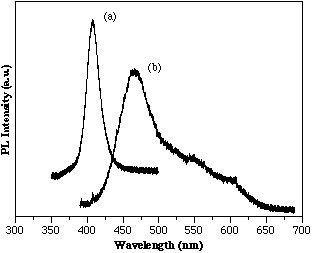
Figure 2. Room temp. PL for (a) In0.15Ga0.85N and (b) In0.35Ga0.65N. (750°C by MOCVD)
The AlInGaN material system has the unique property that the bandgap energy can be engineered to cover wavelengths from the far ultraviolet to the red region of the electromagnetic spectrum. In addition to the problems associated with In desorption and In metal formation discussed previously for In containing compounds, the growth of bulk AlInGaN epitaxial films also has the problem of being more sensitive to the growth temperature. Al-based nitrides favor higher temperatures to obtain good quality material while In-based nitrides require much lower temperatures to aid in In incorporation. We first investigated the MOCVD growth of InGaN and AlGaN at 750°C. This growth temperature seems to be a good compromise for the contradicting requirements for both the Al- and In-containing compounds. The chemical compositions of the AlInGaN quaternary films were obtained by EDS. For calibration of the EDS spectra for In, Al, and Ga, standards made from InGaN and AlGaN films of known compositions was scanned.
Figure 3 shows the θ-2θ x-ray diffraction pattern of a quaternary film indicating a lattice constant of 5.175 Å along the c-axis. The value for the lattice constant can also be determined from the chemical composition of the compound using the formula: Reference Williams, Glisson, Hauser and Littlejohn[8]
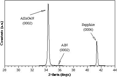
Figure 3. X-ray diffraction for a quaternary film grown by MOCVD at 780°C.
This formula is based on the assumption that a solid solution of the binary constituents is present in the quaternary alloy. For the sample shown in Figure 3, the EDS spectra indicated values of 3% and 10% for InN and AlN, respectively. Reference McIntosh, Boutros, Roberts, Bedair, Piner and El-Masry[4] There is a reasonable agreement between the lattice constants measured by DCXRD and the value deduced from the above equation using the chemical compositions obtained from EDS measurements. Therefore, for the composition range studied thus far, a solid solution exists between the binary constituents. One other point of interest is the lattice constant of this AlInGaN quaternary film closely matches that of GaN making it an excellent candidate for the growth of AlInGaN/GaN lattice-matched heterostructures.
The growth of In-based structures exhibit different growth characteristics than bulk In-based nitrides. Experiments show that thin InGaN heterostructures have higher apparent InN% and no In metal on the surface compared to bulk grown InGaN. This can be attributed to a critical time at growth temperature required to form the critical In metal nucleus size. Above this critical time, In droplets form having deleterious effects on the structure. Below it, In droplets have not formed but instead there is a high density of In atoms on the surface. These will either desorb or incorporate into the film once the top layer growth has begun forming a high InN% film.
AlGaN/InGaN heterostructures show a wavelength shift toward the red compared to bulk InGaN films dependent on the well thickness. Figure 4 shows a series of room temperature PL spectras for AlGaN/InGaN structures. The growth conditions for these films were held constant except the growth time of the active InGaN layer was steadily decreased from (a) to (d). The AlGaN barrier layers were grown with approximately 10% AlN. The graph shows the apparent band edge emission from the active layer corresponding to 400, 456, 505, and 550 nm for (a), (b), (c), and (d), respectively. The FWHMs are 115, 189, 241, and 211 meV, respectively which are comparable to those reported by Nichia obtained from their electroluminescence studies. Although absolute thickness measurements for these samples were not available, TEM data from other similar samples coupled with appropriate scaling of the growth times suggest thicknesses on the order of 25 to 250 Å. The active layers of these films were to thin to obtain x-ray diffraction to verify the InN% indicated by PL (e.g. 65% InN for the 550 nm PL peak.) However, studies into the saturation of the PL peak with increasing laser intensity show evidence that these peaks are band-to-band transitions since no saturation was observed.
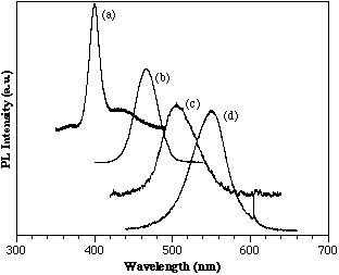
Figure 4. Room temperature PL of MOCVD AlGaN/InGaN/AlGaN double heterostructures.
To reduce the lattice mismatch, AlInGaN/InGaN/AlInGaN heterostructures were grown. Reference McIntosh, Piner, Boutros, Roberts, He, Mousa, El-Masry and Bedair[9] First, DCXRD was used to determine the lattice constants of the ternary and quaternary films when grown separately. The InGaN layer contained 12% InN and the AlInGaN was the same growth conditions as the film shown in Figure 3. From this data the lattice mismatch of the InGaN/AlInGaN interface was determined to be approximately 0.3% for the film whose room temperature PL is shown in Figure 5, indicating band edge emission at 422 nm from the InGaN active layer. The corresponding lattice mismatch of this InGaN film in an AlGaN/InGaN heterostructure would be 1.5%.
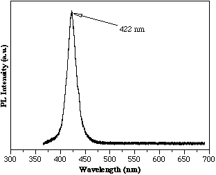
Figure 5. Room temperature PL of a MOCVD AlInGaN/InGaN/AlInGaN heterostructure.
4. Conclusions
InGaN and AlInGaN alloys were epitaxially grown by MOCVD in the compositions range up to 40% InN and 0 - 20% AlN, 0 - 20% InN, respectively. AlGaN/InGaN and AlInGaN/InGaN heterostructures have also been grown and have shown a higher In content than similarly grown bulk InGaN films. Experimental observations on the formation of In metal on the sample surface and ways of controlling this formation was discussed with the main controlling factors indicated to be the growth temperature and EDMIn flux.
Acknowledgments
This work is supported by the Office of Naval Research and the University Research Initiative.


